1/4
TARGET DATA
April, 15 2003
LET9006
RF POWER TRANSISTORS
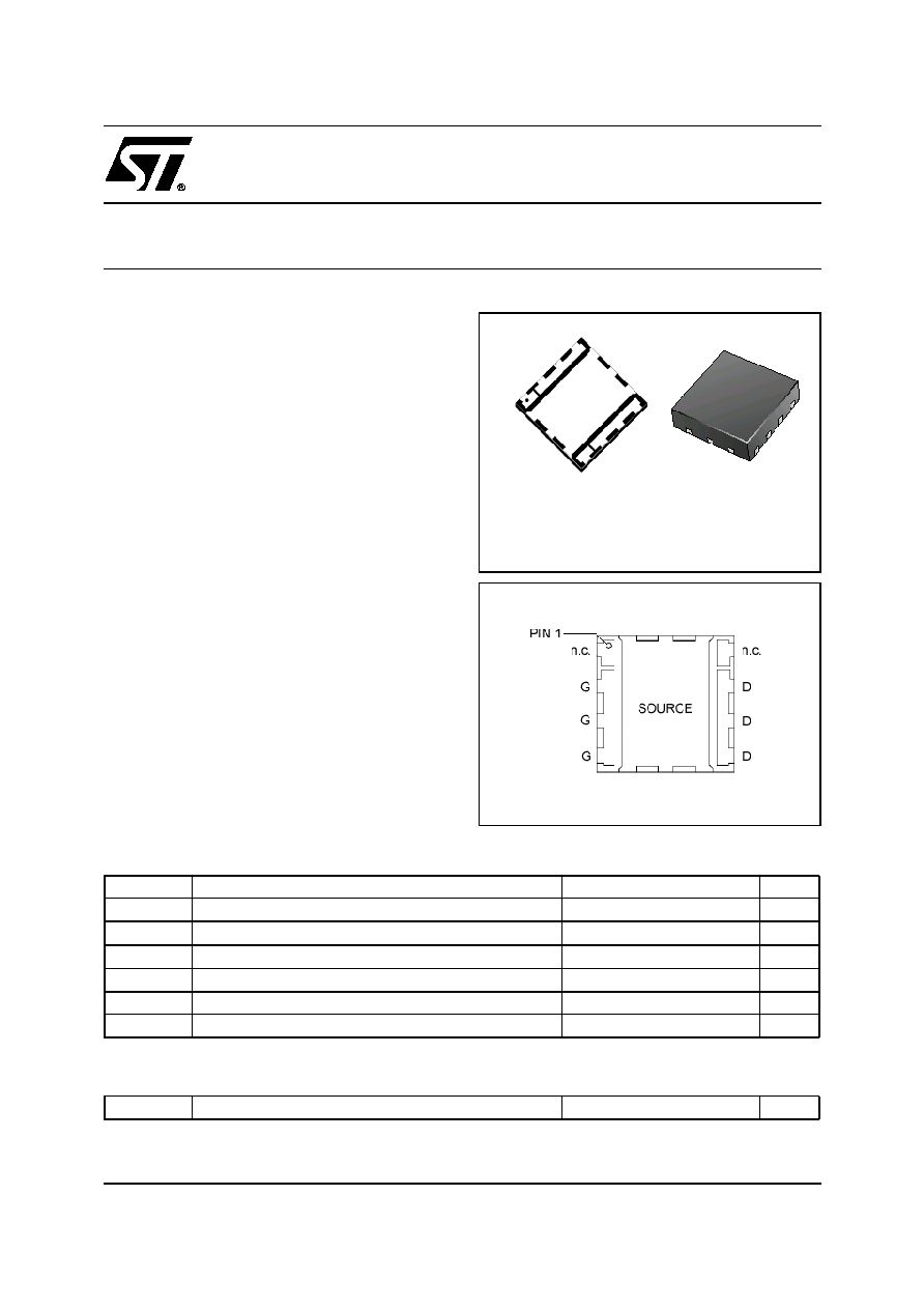
Ldmos Enhanced Technology in Plastic Package
N-CHANNEL ENHANCEMENT-MODE LATERAL
MOSFETs
∑ EXCELLENT THERMAL STABILITY
∑ COMMON SOURCE CONFIGURATION
∑ P
OUT
= 6 W with 17 dB gain @ 960 MHz / 26V
∑ NEW LEADLESS PLASTIC PACKAGE
∑ ESD PROTECTION
∑ SUPPLIED IN TAPE & REEL OF 3K UNITS
DESCRIPTION
The LET9006 is a common source N-Channel, en-
hancement-mode lateral Field-Effect RF power
transistor. It is designed for high gain, broad band
commercial and industrial applications. It operates
at 26 V in common source mode at frequencies up
to 1 GHz. LET9006 boasts the excellent gain,
linearity and reliability of ST's latest LDMOS
technology mounted in the innovative leadless
SMD plastic package, PowerFLATTM.
It is ideal for digital cellular BTS applications
requiring high linearity.
ABSOLUTE MAXIMUM RATINGS (T
CASE
= 25
∞
C)
Symbol
Parameter
Value
Unit
V
(BR)DSS
Drain-Source Voltage
65
V
V
GS
Gate-Source Voltage
-0.5 to +15
V
I
D
Drain Current
1
A
P
DISS
Power Dissipation (@ Tc = 70∞C)
16
W
Tj
Max. Operating Junction Temperature
150
∞C
T
STG
Storage Temperature
-65 to +150
∞C
THERMAL DATA
R
th(j-c)
Junction -Case Thermal Resistance
5
∞C/W
ORDER CODE
LET9006
BRANDING
9006
PowerFLAT
TM
(5x5)
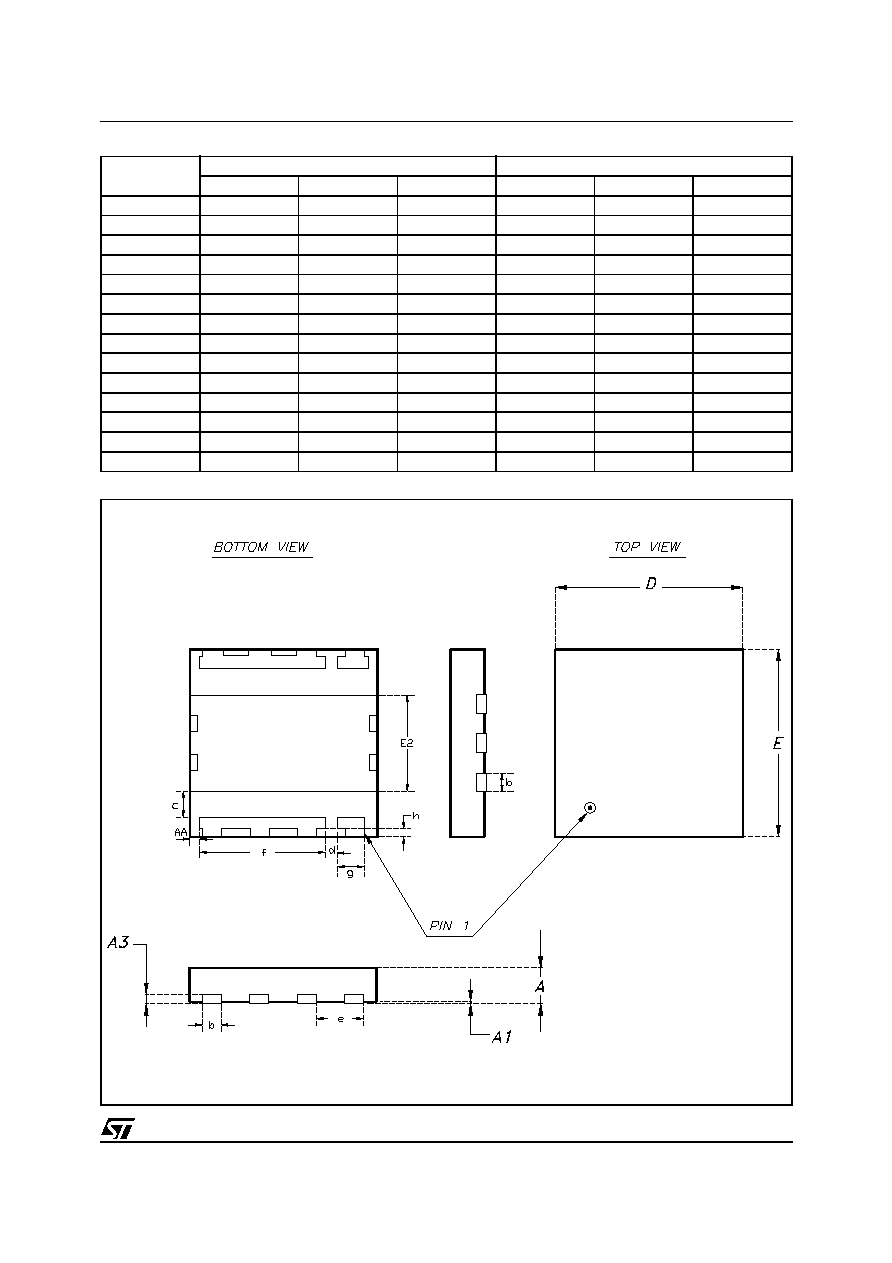
PIN CONNECTION
TOP VIEW
LET9006
2/4
ELECTRICAL SPECIFICATION (T
CASE
= 25
∞
C)
STATIC
DYNAMIC (
f = 960 MHz
)
(1) 1 dB Compression point
DYNAMIC (
f = 920 - 960 MHz
)
(1) 1 dB Compression point
Symbol
Test Conditions
Min.
Typ.
Max.
Unit
V
(BR)DSS
V
GS
= 0 V
I
D
= 1 mA
65
I
DSS
V
GS
= 0 V
V
DS
= 26 V
1
µ
A
I
GSS
V
GS
= 5 V
V
DS
= 0 V
1
µ
A
V
GS(Q)
V
DS
= 26 V
I
D
= TBD
2.0
5.0
V
V
DS(ON)
V
GS
= 10 V
I
D
= 0.5 A
0.9
V
g
FS
V
DS
= 10 V
I
D
= 800 mA
TBD
mho
C
ISS
V
GS
= 0 V
V
DS
= 26 V
f = 1 MHz
TBD
pF
C
OSS
V
GS
= 0 V
V
DS
= 26 V
f = 1 MHz
TBD
pF
C
RSS
V
GS
= 0 V
V
DS
= 26 V
f = 1 MHz
TBD
pF
Symbol
Test Conditions
Min.
Typ.
Max.
Unit
P
OUT
(1)
V
DD
= 26 V
I
DQ
= TBD
7
8
W
D
(1)
V
DD
= 26 V
I
DQ
= TBD
P
OUT
= 6 W
55
65
%
Load
mismatch
V
DD
= 26 V
I
DQ
= TBD
P
OUT
= 6 W
ALL PHASE ANGLES
10:1
VSWR
Symbol
Test Conditions
Min.
Typ.
Max.
Unit
P
out
(1)
V
DD
= 26 V
I
DQ
= TBD
6
7
W
G
P
V
DD
= 26 V
I
DQ
= TBD
P
OUT
= 6 W
17
dB
D
(1)
V
DD
= 26 V
I
DQ
= TBD
P
OUT
= 6 W
55
60
%
LET9006
4/4
Information furnished is believed to be accurate and reliable. However, STMicroelectronics assumes no responsibility for the consequences
of use of such information nor for any infringement of patents or other rights of third parties which may result from its use. No license is granted
by implication or otherwise under any patent or patent rights of STMicroelectronics. Specifications mentioned in this publication are subject
to change without notice. This publication supersedes and replaces all information previously supplied. STMicroelectronics products are not
authorized for use as critical components in life support devices or systems without express written approval of STMicroelectronics.
The ST logo is registered trademark of STMicroelectronics
Æ
2003 STMicroelectronics - All Rights Reserved
All other names are the property of their respective owners.
STMicroelectronics GROUP OF COMPANIES
Australia - Brazil - Canada - China - Finland - France - Germany - Hong Kong - India - Israel - Italy - Japan -
Malaysia - Malta - Morocco - Singapore - Spain - Sweden - Switzerland - United Kingdom - U.S.A.
http://www.st.com