1/6
August 2002
s
LOW OUTPUT CAPACITANCE: 1
µ
F
s
LOW DROP VOLTAGE:
0.5V @ I
O
=1A
1.5V @ I
O
=3A
s
OVERTEMPERATURE PROTECTION
s
OVERCURRENT PROTECTION
s
OUTPUT SHORT CIRCUIT MONITORING,
SIGNALLED BY TTL OUTPUT
s
ON/OFF EXTERNAL CONTROL BY MEANS
OF TTL COMPATIBLE INPUT
s
ADJUSTABLE CURRENT LIMITATION
PROTECTS OUTPUTS FROM DAMAGING
SHORTCIRCUITS
s
REMOTE SENSING OPERATION
DESCRIPTION
The LHC4913 is a positive Voltage Regulator
family
including
both
fixed
and
adjustable
versions. Housed into
SO-20 slug-up package
with stand off zero, it is specifically intended for
applications in rugged environments, such as
Nuclear Physics, in which it has to withstand large
amounts of radiation doses during operating life.
The fixed output voltages available are 2.5, 3.0,
3.3, 5.0 and 8.0V. Input voltage ranges from 3 to
12V.
LHC4913
SERIES
3A POSITIVE LOW DROP VOLTAGE REGULATOR
WITH INHIBIT FUNCTION
This is preliminary information on a new product now in development. Details are subject to change without notice.
SCHEMATIC DIAGRAM
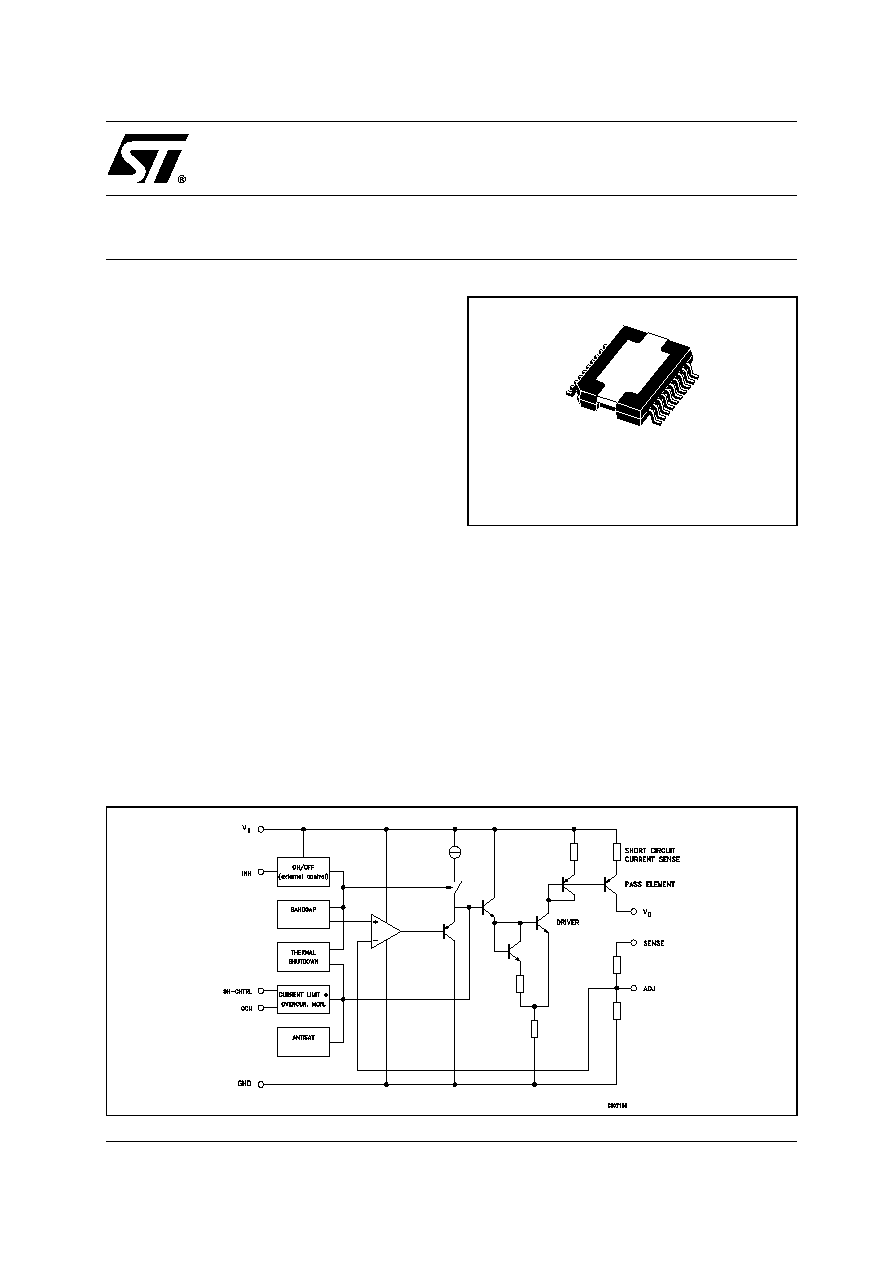
PowerSO-20 slug-up
ADVANCE DATA
LHC4913 SERIES
2/6
ABSOLUTE MAXIMUM RATINGS
Absolute Maximum Ratings are those values beyond which damage to the device may occur. Functional operation under these condition is
not implied.
THERMAL DATA
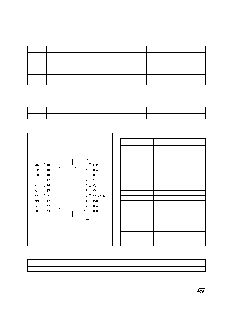
CONNECTION DIAGRAM (top view)
PIN DESCRIPTION FOR ADJUSTABLE
VERSION
ORDERING CODES
Symbol
Parameter
Value
Unit
V
I
DC Input Voltage
14
V
V
INH
INHIBIT Input Voltage
V
I
+ 0.5
V
I
O
Output Current
Internally limited
P
tot
Power Dissipation
Internally limited
T
stg
Storage Temperature Range
-40 to +150
∞C
T
op
Operating Junction Temperature Range
-40 to +125
∞C
Symbol
Parameter
PowerSO-20 slug-up
Unit
R
thj-case
Thermal Resistance Junction-case
2
∞C/W
Pin N∞
Symbol
Name and Function
1
GND
Ground Pin
2
NC
Not Connected
3
NC
Not Connected
4
V
I
Positive Supply Voltage
5
V
O1
Output Pin
6
V
O1
Output Pin
7
SH-CNTRL Short Circuit Valve Controlling
8
OCM
Over Current Monitoring
9
NC
Not Connected
10
GND
Ground Pin
11
GND
Ground Pin
12
INH
Inhibit
13
ADJ
Adjustable pin
14
NC
Not Connected
15
V
O2
Output Pin
16
V
O2
Output Pin
17
V
I
Positive Supply Voltage
18
NC
Not Connected
19
NC
Not Connected
20
GND
Ground Pin
TYPE
Power-SO20 slug-up
OUTPUT VOLTAGES
LHC4913
LHC4913PDU
Adjustable
LHC4913 SERIES
3/6
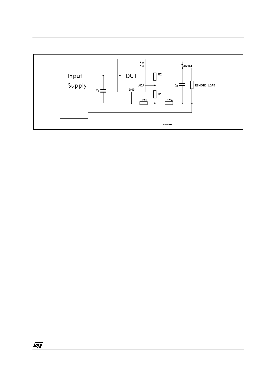
APPLICATION DIAGRAM FOR REMOTE SENSINS OPERATION FOR ADJUSTABLE VERSION
FUNCTIONAL DESCRIPTION
ADJUSTABLE VERSION
The ADJUST pin shall be set at 1.225V with the
adequated fraction of V
O
generated by a resistive
divider inserted between V
O
and GND. The
ADJ-GROUND resistor value must not be greater
than 2.5 K
. For a given V
O
the following holds:
V
O
=V
ADJ
(1+R
2
/R
1
).
OVERTEMPERATURE PROTECTION OPTION
The
LHC4913
is
protected
by
a
junction-
temperature detection circuit, turning the device
"OFF" when the temperature attains 175∞C. The
recovery of the ON mode occurs with a hysteresys
of 40 ∞C.
OVERCURRENT PROTECTION
The device is equipped with a circuit having the
purpose of limiting the maximum load current, in
order to protect the output stage against possible
overcurrent-related damages. Its threshold can be
modified externally by means of a resistor put
between the pins SH-CNTRL and V
I
.
For this characteristic, when the load current gets
close to the above threshold, the regulation is
inhibited. Thus, an excellent operation is granted
only up to 66% of preset maximum current.
SHORT CIRCUIT MONITORING / SIGNALLING
In the event of an overcurrent at the output, a
voltage level of 0.4V is present at the OCM pin. In
others conditions, this voltage equals V
I
.
REMOTE SENSING FOR ADJ VERSION
As pointed out in the pin configuration plot, V
O
and
SENSE are not linked to each other in order to get
a regulation with a load located far away from the
chip. Under ordinary applications, the SENSE
shall be connected to both V
O1
& V
O2
. To obtain
the best performances it is recommended to be
compliant with the configuration shown in the
figure at top page.
What can degrade the regulation performances of
this configuration is the variable voltage drop
between the chip ground and the load termination
Lv.
This is brought mostly by the current Ib coming
from the output power base and going to ground
through the driver stage. The degradation amount
to (1+R
2
/R
1
) x R
W1
x I
Bmax
+ R
W2
x I
Bmax
APPLICATION INFORMATION
Recommended V
I
=12V Max, V
O
= 1.225V Min.
The device is designed to operate with any V
I
-V
O
value according to above mentioned and thermal
dissipation limits.
An input filtering capacitor of 100nF is always
mandatory.
The two V
I
pins shall always be connected in
parallel, this applies also for the four V
O
pins.
Device stability is granted in any circumstance
with a 1
µ
F output capacitor.
The device operation is guaranteed with any
Vin-Vout
dropout
under
the
above
thermal
constraints.
Although
two
embedded
protections
first
mentioned
(the
overtemperature
and
the
overcurrent) ensure the L4913 integrity against
any fault load condition, it is recommended to
comply with the specified absolute maximum
ratings also in applications involving fast switching
of output currents.
To achieve this, a polyester capacitor of at least
470nF, put close to the regulator between input
and ground, improves the L4913 reliability by
LHC4913 SERIES
4/6
filtering the overvoltages spikes coming out during
this particular operation.
To avoid undervoltages spikes leading both input
and output well below ground, it is in addition
recommended to put one reverse-biased Schottky
diodes between output and ground.
ELECTRICAL CHARACTERISTICS (T
J
= 25∞C, V
I
=V
O
+2.5V, V
O
=3V, C
I
= 0.1
µ
F, C
O
= 1
µ
F (tantalium),
unless otherwise specified)
Symbol
Parameter
Test Conditions
Min.
Typ.
Max.
Unit
V
I
Input Voltage
I
O
= 3A
T
J
= -55 to 125
∞C
3
12
V
V
O
Output Voltage
I
O
= 5mA
T
J
= -55 to 125
∞C
2
2
%
I
O
= 3A
T
J
= -55 to 125
∞C
1.23
9
V
I
SHORT
Output Current Limit
Adjustable
3.8
A
V
O
/
V
I
Line Regulation
V
I
= V
O
+2.5V to 12V,
I
O
=
5mA
0.1
%
V
O
/
V
I
Load Regulation
I
O
=
5mA to 3A
0.4
%
V
d
Dropout Voltage
I
O
= 400mA
T
J
= -55 to 125
∞C
0.35
0.7
V
I
O
= 1A
T
J
= -55 to 125
∞C
0.5
1
V
I
O
= 2A
T
J
= -55 to 125
∞C
0.75
1.5
V
I
O
= 3A
T
J
= -55 to 125
∞C
1
2
V
I
d
Quiescent Current
V
I
= V
O
+2.5V to 12V,
On Mode
V
O
= 1.23V
I
O
=
5mA
1.6
4
mA
V
I
= V
O
+2.5V to 12V,
On Mode
V
O
= 1.23V
I
O
=
30mA
2.7
8
mA
V
I
= V
O
+2.5V to 12V,
On Mode
V
O
= 1.23V
I
O
=
300mA
11
24
mA
V
I
= V
O
+2.5V to 12V,
On Mode
V
O
= 1.23V
I
O
=
1A
32
64
mA
V
I
= V
O
+2.5V to 12V,
On Mode
V
O
= 1.23V
I
O
=
2A
64
130
mA
V
I
= V
O
+2.5V to 12V,
On Mode
V
O
= 1.23V
I
O
=
3A
94
200
mA
V
I
= 12V
V
INH
= 3V
Off Mode
0.3
mA
SVR
Supply Voltage Rejection
V
I
= V
O
+2.5V
±
0.5V,
I
O
=
5mA
f = 120Hz
70
dB
f = 33KHz
50
V
INH(OFF)
Turn Off Voltage
T
J
= 0 to 125
∞C
2
V
T
J
= -55 to 0
∞C
2.4
V
V
INH(ON)
Turn On Voltage
T
J
= -55 to 125
∞C
0.8
V
I
INH
Shutdown Input Current
V
I
= 12V
V
INH
= 5V
120
µ
A
C
O
Output Capacitance
I
O
=
5mA to 3A
1
µ
F
ESR
Electrical Series
Resistance
I
O
=
5mA to 3A
2
6
V
OCML
Overcurrent Monitor
Voltage Low
I
OCM
=
10mA (sinked current)V
I
= 12V
0.4
V
V
OCMH
Overcurrent Monitor
Voltage High
I
OCM
=
-10
µ
A
(sourced current)
V
I
= V
O
+2.5V
V
O
+2.5
V
V
I
= 12V
12
eN
Output Noise Voltage
B= 10Hz to 100KHz
I
O
=
1A
66
µ
Vrms/V
LHC4913 SERIES
5/6
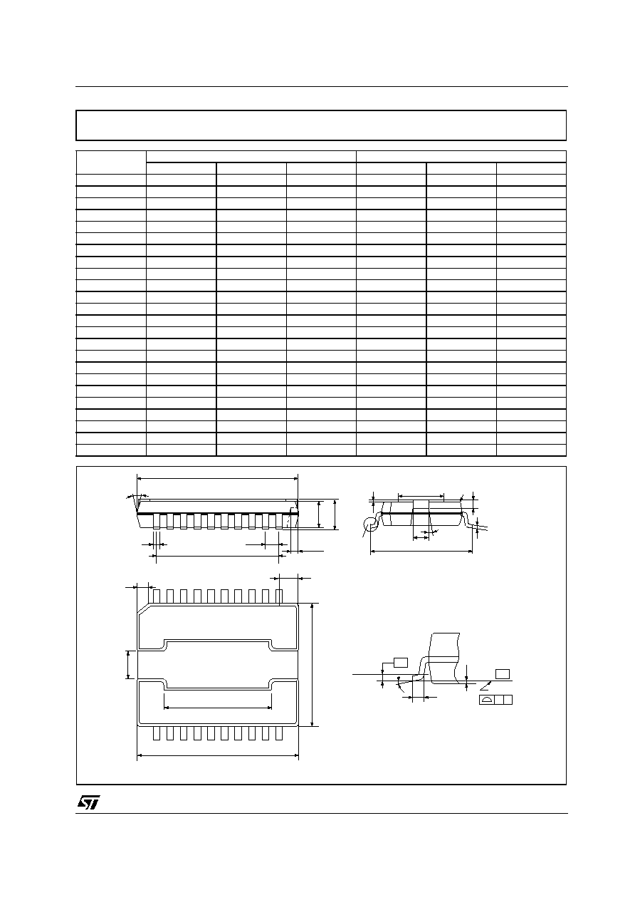
DIM.
mm.
inch
MIN.
TYP
MAX.
MIN.
TYP.
MAX.
A
3.25
3.5
0.128
0.138
a1
3
3.15
3.3
0.118
0.124
0.130
A2
0.1
0.039
A4
0.8
1
0.031
0.039
A5
0.15
0.2
0.25
0.006
0.008
0.010
b
0.4
0.53
0.016
0.021
c
0.23
0.32
0.09
0.013
D
15.8
16
0.622
0.630
D1
9.4
9.8
0.370
0.386
D2
1
0.039
E
13.9
14.5
0.547
0.571
e
1.12
1.27
1.42
0.044
0.050
0.056
e3
11.43
0.450
E1
10.9
11.1
0.429
0.437
E2
2.9
0.114
E3
5.8
6.2
0.228
.0244
G
0
0.1
0.000
0.004
h
1.1
0.043
H
15.5
15.9
0.610
0.626
L
0.8
1.1
0.031
0.043
N
10∞
10∞
R
0.6
0.024
S
0∞
8∞
0∞
8∞
V
5∞
7∞
5∞
7∞
PowerSO-20 Slug-up MECHANICAL DATA
e
A
A2
E
a1
A5
D2 (x2)
M
PSO20DME
D
E1
E2
E2
h x 45∞
S
Gage Plane
0.35
L
DETAIL A
DETAIL A
(COPLANARITY)
G
C
- C -
SEATING PLANE
e3
b
c
N
H
N
V
E3
10
1
D1
20
11
A4
R
0088259-B

LHC4913 SERIES
6/6
Information furnished is believed to be accurate and reliable. However, STMicroelectronics assumes no responsibility for the
consequences of use of such information nor for any infringement of patents or other rights of third parties which may result from
its use. No license is granted by implication or otherwise under any patent or patent rights of STMicroelectronics. Specifications
mentioned in this publication are subject to change without notice. This publication supersedes and replaces all information
previously supplied. STMicroelectronics products are not authorized for use as critical components in life support devices or
systems without express written approval of STMicroelectronics.
© The ST logo is a registered trademark of STMicroelectronics
© 2002 STMicroelectronics - Printed in Italy - All Rights Reserved
STMicroelectronics GROUP OF COMPANIES
Australia - Brazil - Canada - China - Finland - France - Germany - Hong Kong - India - Israel - Italy - Japan - Malaysia - Malta - Morocco
Singapore - Spain - Sweden - Switzerland - United Kingdom - United States.
© http://www.st.com