LM217M
LM317M
MEDIUM CURRENT
1.2 TO 37V ADJUSTABLE VOLTAGE REGULATOR
September 1997
s
OUTPUT VOLTAGE RANGE : 1.2 TO 37V
s
OUTPUT CURRENT IN EXCESS OF 500 mA
s
LINE REGULATION TYP. 0.01%
s
LOAD REGULATION TYP. 0.1%
s
THERMAL OVERLOAD PROTECTION
s
SHORT CIRCUIT PROTECTION
s
OUTPUT TRANSISTOR SAFE AREA
COMPENSATION
s
FLOATING OPERATION FOR HIGH
VOLTAGE APPLICATIONS
DESCRIPTION
The LM217M/LM317M are monolithic integrated
circuits in TO-220, DPAK, SOT-82 and SOT-194
packages intended for use as positive adjustable
voltage regulators.
They are designed to supply until 500 mA of load
current with an output voltage adjustable over a
1.2 to 37V range.
The nominal output voltage is selected by means
of only a resistive divider, making the device
exceptionally easy to use and eliminating the
stocking of many fixed regulators.
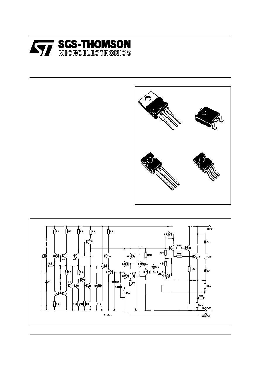
SCHEMATIC DIAGRAM
SOT-82
SOT-194
DPAK
TO-252
TO-220
1/11

TEST CIRCUIT
ABSOLUTE MAXIMUM RATINGS
Symbol
Parameter
Value
Unit
V
i
- V
o
Input-Output Differential Voltage
40
V
P
d
Power Dissipation
I nternally Limited
T
o pr
Operating Junction Temperature Range (*)
for LM217M
for LM317M
-40 to 125
0 to 125
o
C
o
C
T
stg
Storage Temperature Range
-55 to 150
o
C
(*) Re-Boot is not guaranteed for T
j
85
o
C
PIN CONNECTION AND ORDERING NUMBERS
TO-220
SOT-82
Type
TO-220
DPAK
SOT-82
SOT-194
LM217M
LM217MT
LM217MDT
LM217MX
LM217MS
LM317M
LM317MT
LM317MDT
LM317MX
LM317MS
DPAK
SOT-194
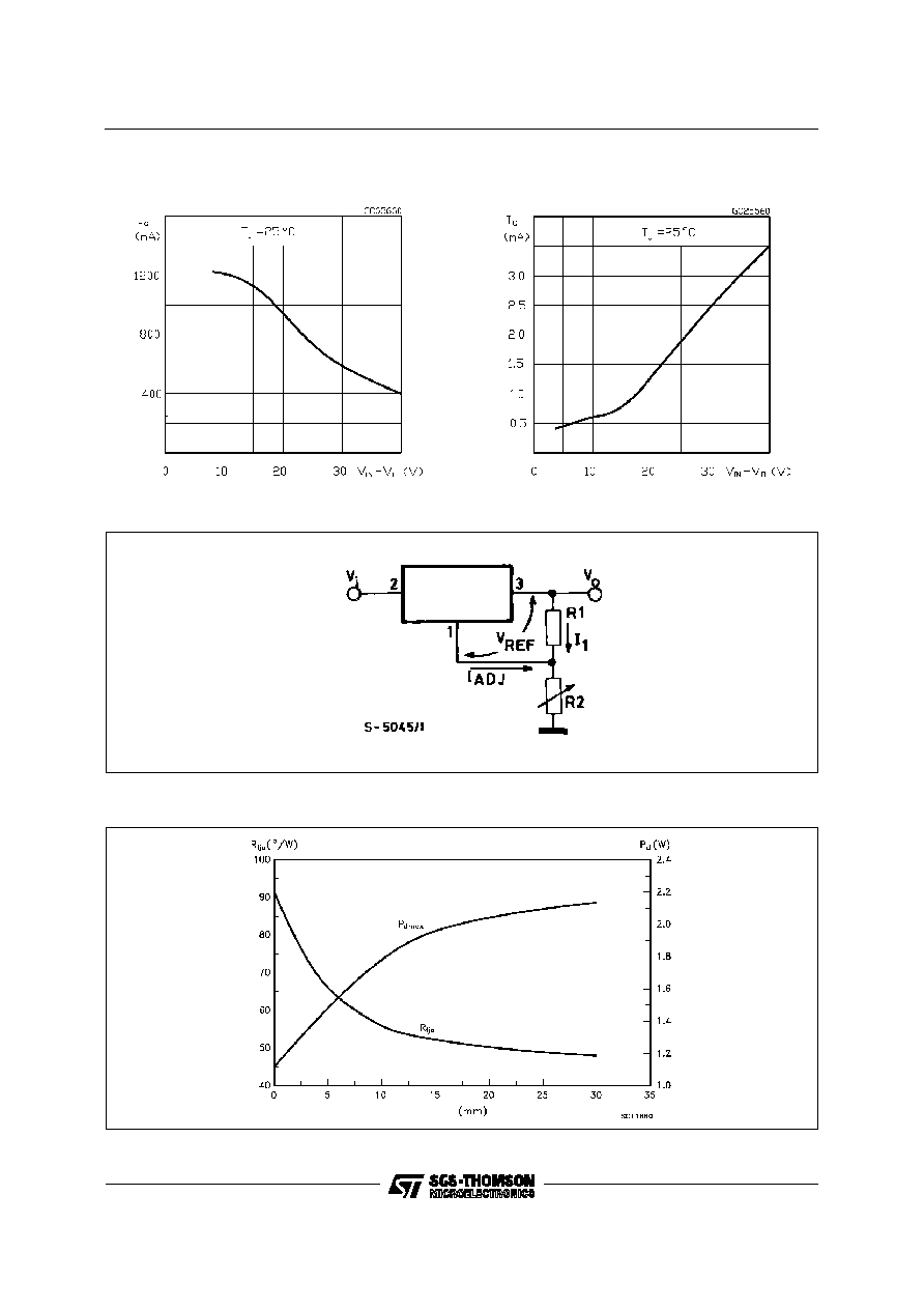
THERMAL DATA
Symbol
Parameter
SOT-82
SOT-194
DPAK
TO-220
Unit
R
thj-ca se
R
thj-a mb
Thermal Resistance Junction-case
Max
Thermal Resistance Junction-ambient
Max
8
100
3
50
o
C/W
o
C/W
LM217M/LM317M
2/11
(*) CADJ is connected between Adjust pin and Ground.
ELECTRICAL CHARACTERISTICS FOR LM317M (Refer to the test circuits, 0
T
j
125
o
C
V
i
- V
o
= 5 V, I
o
= 100 mA, P
d
7.5W, unless otherwise specified)
Symbol
Parameter
Test Conditions
Min.
Typ.
Max.
Unit
V
o
Line Regulation
V
i
- V
o
= 3 to 40 V
T
j
= 25
o
C
0.01
0.04
%/V
0.02
0.07
%/V
V
o
Load Regulation
V
o
5V
I
o
= 10 mA to 500 mA
T
j
= 25
o
C
5
25
mV
20
70
mV
V
o
5V
I
o
= 10 mA to 500 mA
T
j
= 25
o
C
0.1
0.5
%/V
o
0.3
1.5
%/V
o
I
ADJ
Adjustment Pin Current
50
100
µ
A
I
ADJ
Adjustment Pin Current
V
i
- V
o
= 3 to 40 V
I
o
= 10 mA to 500 mA
0.2
5
µ
A
V
REF
Reference Voltage
V
i
- V
o
= 3 to 40 V
I
o
= 10 mA to 500 mA
1.2
1.25
1.3
V
V
o
V
o
Output Voltage Temperature
Stability
0.7
%
I
o(min)
Minimum Load Current
V
i
- V
o
= 40 V
3.5
10
mA
I
o( max)
Maximum Output Current
V
i
- V
o
15V
V
i
- V
o
=40V, P
d
< P
dMAX
, T
j
=25
o
C
500
1000
200
mA
e
N
Output Noise Voltage
(percentance of V
O
)
B = 10Hz to 10KHz
T
j
= 25
o
C
0. 003
%
SVR
Supply Voltage Rejection (*)
T
j
= 25
o
C
f = 120 Hz
C
ADJ
=0
65
dB
C
ADJ
=10
µ
F
66
80
dB
(*) CADJ is connected between Adjust pin and Ground.
ELECTRICAL CHARACTERISTICS FOR LM217M (Refer to the test circuits, -40
T
j
125
o
C
V
i
- V
o
= 5 V, I
o
= 100 mA, P
d
7.5W, unless otherwise specified)
Symbol
Parameter
Test Conditions
Min.
Typ.
Max.
Unit
V
o
Line Regulation
V
i
- V
o
= 3 to 40 V
T
j
= 25
o
C
0.01
0.02
%/V
0.02
0.05
%/V
V
o
Load Regulation
V
o
5V
I
o
= 10 mA to 500 mA
T
j
= 25
o
C
5
15
mV
20
50
mV
V
o
5V
I
o
= 10 mA to 500 mA
T
j
= 25
o
C
0.1
0.3
%/V
o
0.3
1
%/V
o
I
ADJ
Adjustment Pin Current
50
100
µ
A
I
ADJ
Adjustment Pin Current
V
i
- V
o
= 3 to 40 V
I
o
= 10 mA to 500 mA
0.2
5
µ
A
V
REF
Reference Voltage
V
i
- V
o
= 3 to 40 V
I
o
= 10 mA to 500 mA
1.2
1.25
1.3
V
V
o
V
o
Output Voltage Temperature
Stability
0.7
%
I
o(min)
Minimum Load Current
V
i
- V
o
= 40 V
3.5
5
mA
I
o( max)
Maximum Output Current
V
i
- V
o
15V
V
i
- V
o
=40V, P
d
< P
dMAX
, T
j
=25
o
C
500
1000
200
mA
e
N
Output Noise Voltage
(percentance of V
O
)
B = 10Hz to 10KHz
T
j
= 25
o
C
0. 003
%
SVR
Supply Voltage Rejection (*)
T
j
= 25
o
C
f = 120 Hz
C
ADJ
=0
65
dB
C
ADJ
=10
µ
F
66
80
dB
LM217M/LM317M
3/11

APPLICATION INFORMATION
The LM317M provides an internal reference
voltage of 1.25V between the
output and
adjustments terminals. This is used to set a
constant current flow across an external resistor
divider (see fig. 3), giving an output voltage V
O
of:
V
O
= V
REF
(
1
+
R
2
R
1
)
+ I
ADJ
R
2
The device was designed to minimize the term
I
ADJ
(100
µ
A max) and to maintain it very constant
with line and load changes. Usually, the error
term IADJ
R2 can be neglected. To obtain the
previous requirement, all the regulator quiescent
current is returned to the output terminal,
imposing a minimum load current condition. If the
load is insufficient, the output voltage will rise.
Since the LM317M is a floating regulator and
"sees" only the input-to-output differential voltage,
supplies of very high voltage with respect to
ground can be regulated as long as the maximum
input-to-output differential
is
not
exceeded.
Furthermore, programmable regulator are easily
obtainable and, by connecting a fixed resistor
between the adjustment and output, the device
can be used as a precision current regulator.
In order to optimise the load regulation, the
current set resistor R1 (see fig. 3) should be tied
as close as possible to the regulator, while the
ground terminal of R2 should be near the ground
of the load to provide remote ground sensing.
EXTERNAL CAPACITORS (Fig.5)
Normally no capacitors are needed unless the
device is situated far from the input filter
capacitors; in which case an input bypass is
needed.
A 0.1
µ
F disc or 1
µ
F tantalium input bypass
capacitor (C
I
) is recommended to reduce the
sensitivity to input line impedance.
The adjustment terminal may be bypassed to
ground to improve ripple rejection. This capacitor
(C
adj
) prevents ripple from being amplified as the
output voltage is increased. A 10
µ
F capacitor
should improve ripple rejection about 80dB at
120Hz an a 10V application.
Although the LM317M is stable with no output
capacitance like any feedback circuit, certain
values
of
external
capacitance
can
cause
excessive ringing. An output capacitance (C
O
) in
the form of a 1
µ
F tantalium or 25
µ
F aluminium
electrolytic capacitor on the output swamps this
effect and insures stability.
PROTECTION DIODES (Fig.5)
When external capacitors are used with any IC
regulator it is sometimes necessary to add
protection diodes to prevent the capacitors from
discharging through low current points into the
regulator.
Figure
5
show
the
LM317M
with
the
recommended
protection
diodes
for
output
voltages in excess of 25V or high capacitance
values (C
3
> 25
µ
F, C
2
> 10
µ
F). Diode D1
prevents C
3
from discharging through the IC
during an input short-circuit. The combination of
diodes D1 and D2 prevents C
2
from discarging
through the regulator during an input or output
short-circuit.
START-UP BLOCK
It's not guaranteed the Re-Boot of the device
when the junction temperature is over 85
o
C.
LM217M/LM317M
5/11