LM150/250
LM350
March 1993
ADJUSTABLE VOLTAGE REGULATORS
THREE-TERMINAL 3 A
.
GUARANTEED 3A OUTPUT CURRENT
.
ADJUSTABLE OUTPUT DOWN TO 1.2V
.
LINE REGULATION TYPICALLY 0.005% /V
.
LOAD REGULATION TYPICALLY 0.1%
.
GUARANTEED THERMAL REGULATION
.
CURRENT LIMIT CONSTANT WITH TEM-
PERATURE
.
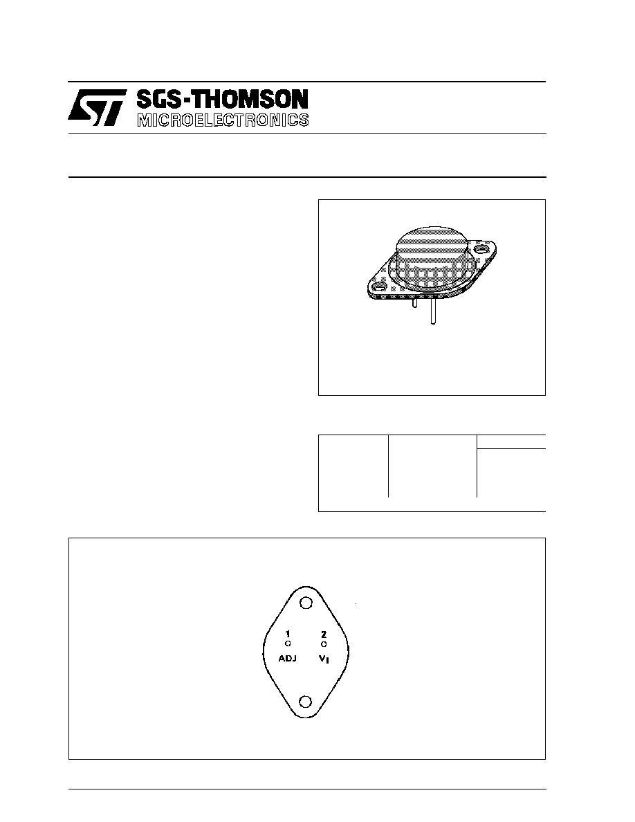
STANDARD 3-LEAD TRANSISTOR PACKAGE
TO3
K SUFFIX
(Steel Can)
ORDER CODE
PART
NUMBER
TEMPERATURE
RANGE
PACKAGE
K
LM150
LM250
LM350
-55
o
C to + 150
o
C
-25
o
C to + 150
o
C
0
o
C to + 125
o
C
∑
∑
∑
EXAMPLE: LM150K
PIN CONNECTION
(bottom view)
Case is output
1/7
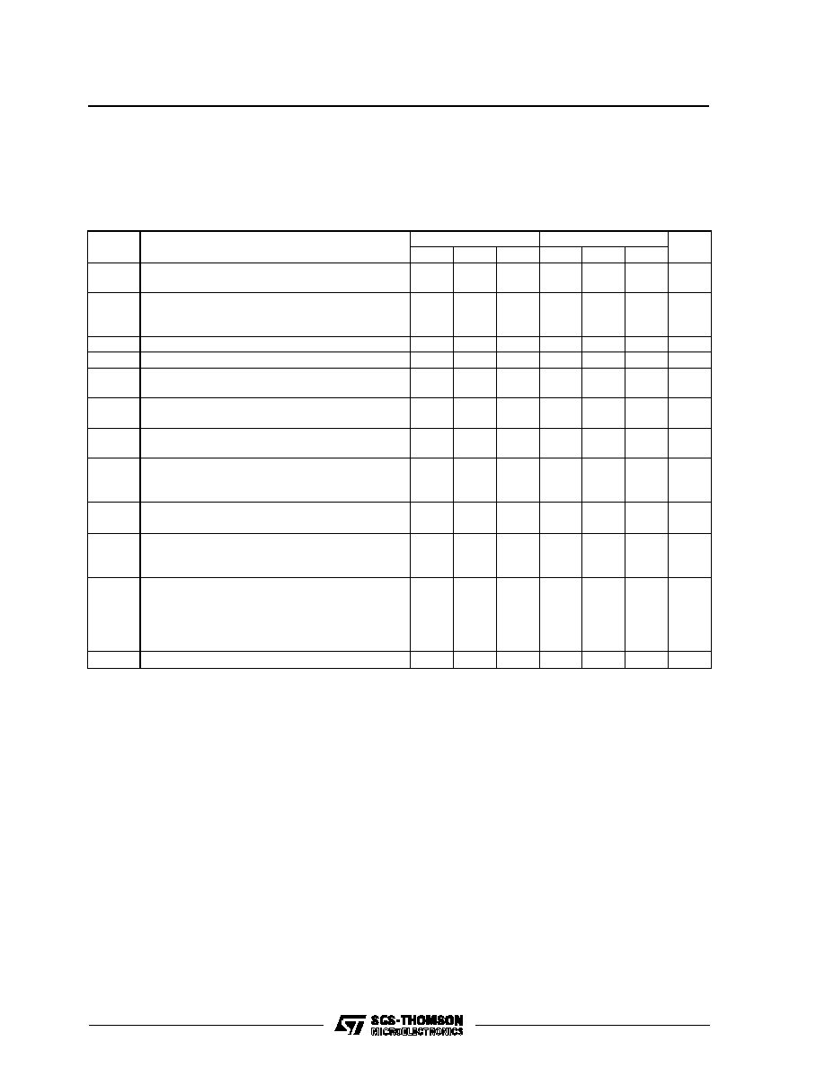
ELECTRICAL CHARACTERISTICS
LM150: -55
o
C
T
j
150
o
C, V
I
- V
O
= 5V, I
O
= 1.5A
LM250: -25
o
C
T
j
150
o
C, V
I
- V
O
= 5V, I
O
= 1.5A
LM350: 0
o
C
T
j
150
o
C, V
I
- V
O
= 5V, I
O
= 1.5A
Although power dissipation is internally limited, these specifications apply to power dissipation up to
30W (unless otherwise specified).
Symbol
Parameter
LM150-LM250
LM350
Unit
Min.
Typ.
Max.
Min.
Typ.
Max.
K
VI
Line Regulation - (note 1)
T
amb
= 25
o
C, 3 V
(V
I
- V
O
)
35 V
0.005
0.01
0.005
0.03
%/V
K
VO
Load Regulation T
amb
= 25
o
C, 10 mA
I
O
3 A
V
O
5V - (note 1)
V
O
5V - (note 1)
5
0.1
15
0.3
5
0.1
25
0.5
mV
%
Thermal Regulation (pulse = 20 ms)
0.002
0.01
0.002
0.02
%/W
I
adj
Adjustment Pin Current
50
100
50
100
µ
A
I
adj
Adjustment Pin Current Change
10 mA
I
L
3 A, 3 V
(V
I
- V
O
)
35 V
0.2
5
0.2
5
µ
A
v
(ref)
Reference Voltage
3V
(V
I
- V
O
)
35 V, 10 mA
I
O
3A, P
30W
1.19
1.24
1.29
1.19
1.24
1.29
V
K
VI
Line Regulation - (note 1)
3 V
(V
I
- V
O
)
35 V
0.02
0.05
0.02
0.05
%/V
K
VO
Load Regulation 10 mA
I
O
3 A
V
O
5V - (note 1)
V
O
5V - (note 1)
20
0.3
50
1
20
0.3
70
1.5
mV
%
K
VT
Temperature Stability (T
min
T
j
T
max
)
1
1
%
I
O(min)
Minimum Load Current (V
I
- V
O
35 V)
3.5
5
3.5
10
mA
I
O(max)
Current Limit (V
I
- V
O
10 V)
DC
V
I
- V
O
= 30 V
3
4.5
1
3
4.5
1
A
RMS Output Noise, % of V
O
(T
amb
= 25
o
C, 10 Hz
f
10 KHz)
0.001
0.001
%
R
vf
Ripple Rejection Ratio
V
O
= 10 V, f = 120 Hz
C
adi
= 10
µ
F
66
65
86
66
65
86
dB
K
VH
Long Term Stability (T
amb
= 125
o
C)
0.3
1
0.3
1
%
Note 1 : Regulation is measured at constant junction temperature. Changes in output voltage due to heating effects are taken
into account separately by thermal rejection.
LM150-LM250-LM350
3/7

TYPICAL APPLICATIONS
+ 1.2V to + 25V ADJUSTABLE REGULATOR
APPLICATION HINTS
In operation, the LM350 develops a nominal 1.25V
reference voltage, V
(ref)
, between the output and
adjustment terminal. The reference voltage is im-
pressed across program resistor R1 and, since the
voltage is constant, a constant current I
1
then flows
through the output set resistor R2, giving an output
voltage of
V
O
= V
(ref)
( 1+
R
2
R
1
) + I
adj
R
2
Figure 1.
Since the 50
µ
A current from the adjustment termi-
nal represents an error term, the LM350 was de-
signed to minimize I
adj
and make it very constant
with line and load changes. To do this, all quiescent
operating current is returned to the output establi-
shing a minimum load current requirement. If there
is insufficient load on the output, the output will rise.
EXTERNAL CAPACITORS
An input bypass capacitor is recommended. A
0.1
µ
F disc or 1
µ
F solid tantalum on the input is suit-
able input by passing for almost all applications.
The device is more sensitive to the absence of input
bypassing when adjustment or output capacitors
are used byt the above values will eliminate the
possibility of problems.
The adjustment terminal can be bypassed to
ground on the LM350 to improve ripple rejection.
This bypass capacitor prevents ripple form being
amplified as the output voltage is increased. With
a 10
µ
F bypass capacitor 75dB ripple rejection is
obtainable at any output level. Increases over 20
µ
F
do not appreciably improve the ripple rejection at
frequencies above 120Hz. If the bypass capacitor
is used, it is sometimes necessary to include pro-
tection diodes to prevent the capacitor from dis-
charging through internal low current paths and
damaging the device.
In general, the best type of capacitors to use are
solid tantalum. Solid tantalum capacitors have low
impedance even at high frequencies. Depending
upon capacitor construction, it takes about 25
µ
F in
aluminum electrolytic to equal 1
µ
F solid tantalum at
high frequencies. Ceramic capacitors are also
good at high frequencies, but some types have a
large decrease in capacitance at frequencies
around 0.5MHz. For this reason, 0.01
µ
F disc may
seem to work better than a 0.1
µ
F disc as a bypass.
Although the LM350 is stable with no output capa-
citors, like any feedback circuit, certain values of
external capacitance can cause excessive ringing.
This occurs with values between 500pF and
5000pF. A 1
µ
F solid tantalum (or 25
µ
F aluminium
electrolytic) on the output swamps this effect and
insures stability.
LOAD REGULATION
The LM350 is capable of providing extremely good
load regulation but a few precautions are needed
to obtain maximum performance. The current set
resistor connected between the adjustment termi-
nal and the output terminal (usually 240
) should
be tied directly to the output of the regulator rather
than near the load. This eliminates line drops from
appearing effectively in series with the reference
and degrading regulation. For example, a 15V
regulator with 0.05
resistance between the regu-
lator and load will have a load regulation due to line
resistance of 0.05
x I
L
. If the set resistor is con-
nected near the load the effective line resistance
Needed if device is far from filter capacitors.
* Optional-improves transient response. Output capacitors in the
range of 1
µ
F to 100
µ
F of aluminium or tantalum electrolytic are
commonly used to provide improved output impedance and rejec-
tion of transients.
R2
* * V
O
= 1.25V ( 1 +
)
R1
* * * R1 = 240
for LM150 and LM250
LM350
LM350
LM150-LM250-LM350
4/7
will be 0.05
(1 + R
2
/R
1
) or in this case, 11.5 times
worse.
Figure 2 shows the effect of resistance between the
regulator and 140
set resistor.
With the TO-3 package, it is easy to minimize the re-
sistance from the case to the set resistor, by using
2 separate leads to the case. The ground of R2 can
be returned near the ground of the load to provide
remote ground sensing and improve load regula-
tion.
PROTECTION DIODES
When external capacitors are used with any IC regu-
lator it is sometimes necessary to add protection
diodes to prevent the capacitors from discharging
through low current points into the regulator. Most
Figure 2 : Regulator with Line Resistance in Out-
put Lead.
20
µ
F capacitors have low enough internal series re-
sistance to deliver 20A spikes when shorted. Al-
though the surge is short, there is enough energy to
damage parts of the IC.
When an output capacitor is connected to a regula-
tor and the input is shorted, the output capacitor will
discharge into the output of the regulator. The dis-
charge current depends on the value of the capaci-
tor, the output voltage of the regulator, and the rate
of decrease of V
I
. In the LM350 this discharge path
is through a large junction that is able to sustain 25A
surge with no problem. This is not true of other types
of positive regulators. For output capacitors of
100
µ
F or less at output of 15V or less, there is no
need to use diodes.
The bypass capacitor on the adjustment terminal
can discharge through a low current junction. Dis-
charge occurs when either the input or output is
shorted. Internal to the LM350 is a 50
resistor
which limits the peak discharge current. No protec-
tion is needed for output voltages of 25V or less and
10
µ
F capacitance. Figure 3 shows an LM350 with
protection diodes included for use with outputs
greater than 25V and high values of output capacit-
ance.
Figure 3 : Regulator with Protection Diodes.
LM350
LM350
LM150-LM250-LM350
5/7
