 | –≠–ª–µ–∫—Ç—Ä–æ–Ω–Ω—ã–π –∫–æ–º–ø–æ–Ω–µ–Ω—Ç: LM723N | –°–∫–∞—á–∞—Ç—å:  PDF PDF  ZIP ZIP |

LM723
HIGH PRECISION VOLTAGE REGULATOR
September 1998
s
INPUT VOLTAGE UP TO 40V
s
OUTPUT VOLTAGE ADJUSTABLE FROM 2
TO 37V
s
POSITIVE OR NEGATIVE SUPPLY
OPERATION
s
SERIES, SHUNT, SWITCHING OR
FLOATING OPERATION
s
OUTPUT CURRENT TO 150mA WITHOUT
EXTERNAL PASS TRANSISTOR
s
ADJUSTABLE CURRENT LIMITING
DESCRIPTION
The
LM723
is
a
monolithic
integrated
programmable voltage regulator, assembled in
14-lead
dual
in-line
plastic
and
SO-14
micropackage.
The
circuit
provides
internal
current limiting. When the output current excedes
150mA an external NPN or PNP pass element
may be used. Provisions are made for adjustable
current limiting and remote shut-down.
Æ
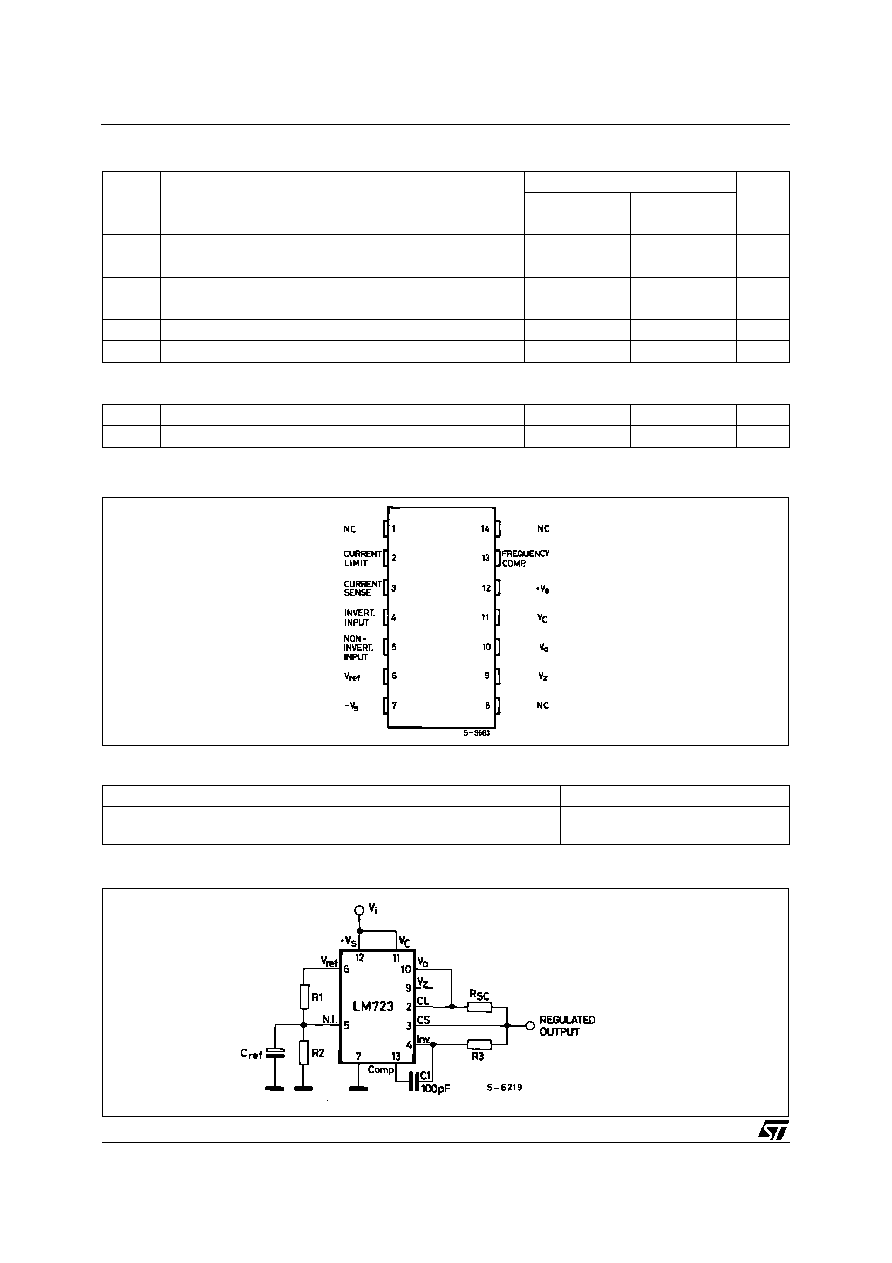
BLOCK DIAGRAM
Plastic DIP-14
SO-14
1/12

ABSOLUTE MAXIMUM RATINGS
Symbol
Parameter
Value
Unit
LM723
LM723C
V
i
DC Input Voltage
40
40
V
V
i-o
Dropout Voltage
40
40
V
I
o
Output Current
150
150
mA
I
ref
Current from V
ref
15
25
mA
T
o p
Operating Temperature
-55 to 125
0 to 70
o
C
T
stg
Storage Temperature
-65 to 150
-65 to 150
o
C
T
j
Junction Temperature
150
125
o
C
PIN CONNECTION (top views)
ABSOLUTE MAXIMUM RATINGS
Symbol
Parameter
Plastic DIP-14
SO-14
Unit
R
thj-a mb
Thermal Resistance Junction-Ambient
Max
200
160
o
C/W
TEST CIRCUIT (pin configuration relative to the plastic package)
V
i
= 12V
V
o
= 5V
I
o
= 1mA
R
1
/R
2
10K
ORDER CODES
Type
Plastic DIP-14
SO-14
LM723
LM723C
LM723N
LM723CN
LM723CD
LM723
2/12

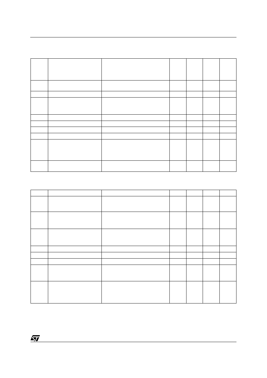
ELECTRICAL CHARACTERISTICS FOR LM723C (refer to the test circuits, T
amb
= 25
o
C,
unless otherwise specified)
Symbol
Parameter
Test Conditions
Min.
Typ.
Max.
Unit
V
o
/
V
i
Line Regulation
V
i
= 12 to 15V
V
i
= 12 to 40V
V
i
= 12 to 15V
0
o
C
T
amb
70
o
C
0.01
0. 1
0.1
0.5
0.3
%
%
%
V
o
/V
o
Load Regulation
I
o
= 1 to 50 mA
I
o
= 1 to 10 mA
0
o
C
T
amb
70
o
C
0.03
0.2
0.6
%
%
V
REF
Reference Voltage
I
ref
= 160
µ
A
6.8
7.15
7.5
V
SVR
Supply Voltage Rejection
f = 100 Hz to 10 KHz
C
ref
= 0
f = 100 Hz to 10 KHz
C
ref
= 5
µ
F
74
86
dB
dB
V
o
/
T Output Voltage Drift
150
ppm/
o
C
I
sc
Output Current Limit
R
sc
= 10
V
o
= 0
65
mA
V
i
Input Voltage Range
9.5
40
V
V
o
Output Voltage Range
2
37
V
V
o
-V
i
3
38
V
I
d
Quiescent Current
V
i
= 30 V I
o
= 0 mA
2. 3
4
mA
K
VH
Long Term Stability
0. 1
%/ 1000
hrs
e
N
Output Noise Voltage
BW = 100 Hz to 10 KHz
C
ref
= 0
BW = 100 Hz to 10 KHz
C
ref
= 5
µ
F
20
2. 5
µ
V
µ
V
ELECTRICAL CHARACTERISTICS FOR LM723 (refer to the test circuits, T
amb
= 25
o
C,
unless otherwise specified)
Symbol
Parameter
Test Conditions
Min.
Typ.
Max.
Unit
V
o
/
V
i
Line Regulation
V
i
= 12 to 15V
V
i
= 12 to 40V
V
i
= 12 to 15V
-55
o
C
T
amb
125
o
C
0.01
0.02
0.1
0.2
0.3
%
%
%
V
o
/V
o
Load Regulation
I
o
= 1 to 50 mA
I
o
= 1 to 10 mA
-55
o
C
T
amb
125
o
C
0.03
0.15
0.6
%
%
V
REF
Reference Voltage
I
ref
= 160
µ
A
6.95
7.15
7.35
V
SVR
Supply Voltage Rejection
f = 100 Hz to 10 KHz
C
ref
= 0
f = 100 Hz to 10 KHz
C
ref
= 5
µ
F
74
86
dB
dB
V
o
/
T Output Voltage Drift
150
ppm/
o
C
I
sc
Output Current Limit
R
sc
= 10
V
o
= 0
65
mA
V
i
Input Voltage Range
9.5
40
V
V
o
Output Voltage Range
2
37
V
V
o
-V
i
3
38
V
I
d
Quiescent Current
V
i
= 30 V I
o
= 0 mA
2. 3
5
mA
K
VH
Long Term Stability
0. 1
%/ 1000
hrs
e
N
Output Noise Voltage
BW = 100 Hz to 10 KHz
C
ref
= 0
BW = 100 Hz to 10 KHz
C
ref
= 5
µ
F
20
2. 5
µ
V
µ
V
LM723
3/12

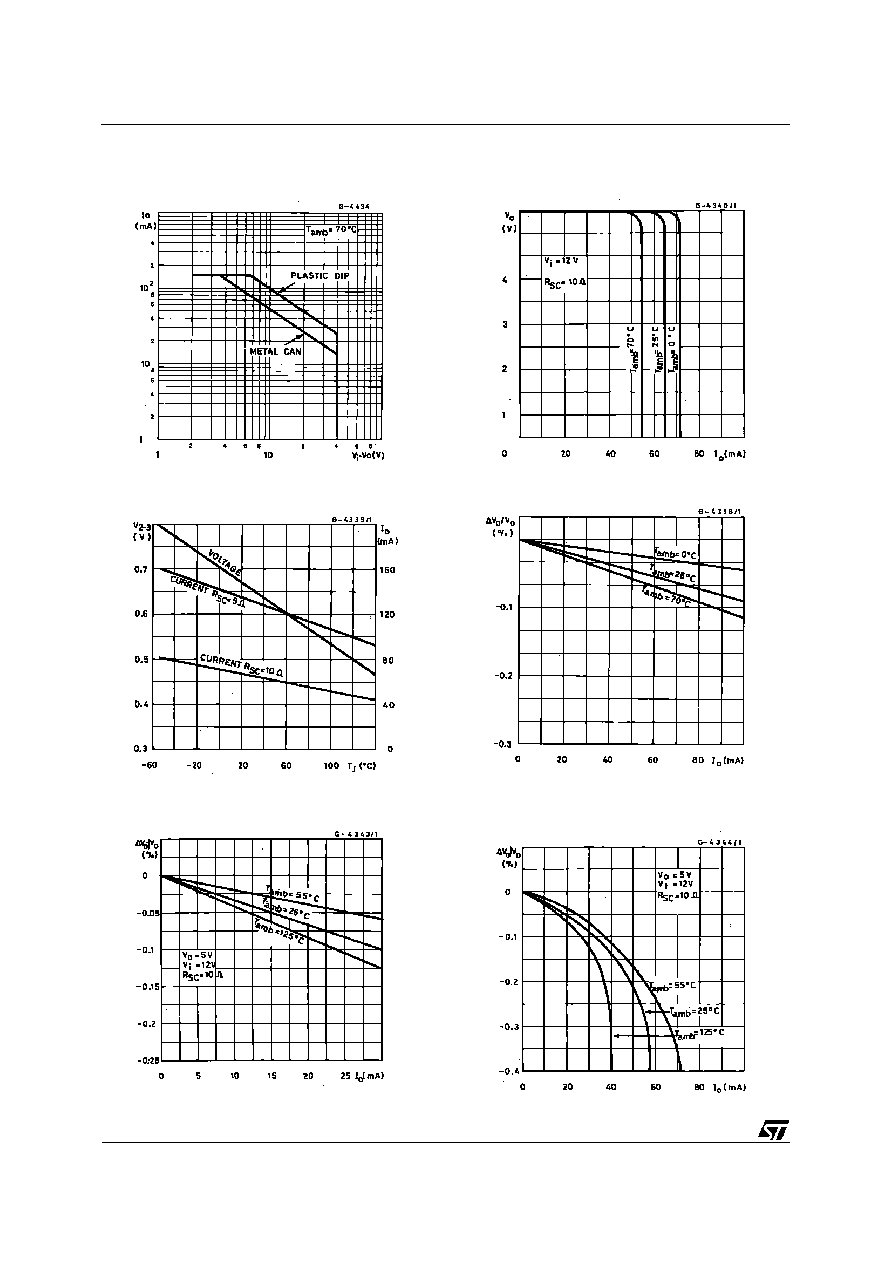
Figure 3 : Current Limiting Characteristics vs.
Junction Temperature.
Figure 4 : Load Regulation Characteristics
without Current Limiting.
Figure 5 : Load Regulation Characteristics with
Current Limiting.
Figure 6 : Load Regulation Characteristics with
Current Limiting
Figure 1 : Maximum Output Current vs. Voltage
Drop.
Figure 2 : Current Limiting Characteristics.
LM723
4/12

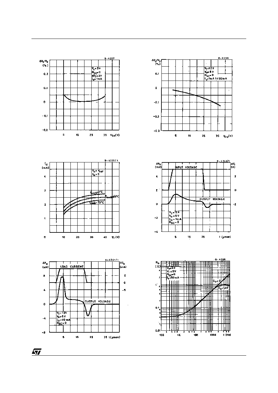
Figure 9 : Quiescent Drain Current vs. Input
Voltage.
Figure 10 : Line Transient Response.
Figure 11 : Load Transient Response.
Figure 12 : Output Impedance vs. Frequency.
Figure 7 : Line Regulation vs. Voltage Drop.
Figure 8 : Load Regulation vs. Voltage Drop.
LM723
5/12

