 | –≠–ª–µ–∫—Ç—Ä–æ–Ω–Ω—ã–π –∫–æ–º–ø–æ–Ω–µ–Ω—Ç: M2201 | –°–∫–∞—á–∞—Ç—å:  PDF PDF  ZIP ZIP |

M2201
2-Wires 1 Kbit (x8) Serial EEPROM
July 1999
1/15
AI01321
WC
VCC
M2201
VSS
SDA
SCL
Figure 1. Logic Diagram
TWO WIRE SERIAL INTERFACE
100.000 ERASE/WRITE CYCLES with
100 YEARS DATA RETENTION at 55
∞
C
SINGLE SUPPLY VOLTAGE:
≠ 4.5V to 5.5V for M2201 version
≠ 2.7V to 5.5V for M2201V version
HARDWARE WRITE CONTROL
100 KBIT TRANSFER RATE
BYTE WRITE
PAGE WRITE (up to 4 BYTES)
SELF TIMED PROGRAMMING CYCLE
AUTOMATIC ADDRESS INCREMENTING
ENHANCED ESD/LATCH UP
DESCRIPTION
The M2201 is a simplified 2-wire bus 1 Kbit electri-
cally erasable programmable memory (EEPROM),
organized as 128 x8 bits. It is manufactured in
STMicroelectronics's Hi-Endurance Advanced
CMOS technology which guarantees a data reten-
tion of 100 years at 55
∞
C.
The M2201 is available in Plastic Dual-in-Line,
Plastic Small Outline and Thin Shrink Small Out-
line packages.
The memory is compatible with a two wire serial
interface which uses a bi-directional data bus and
serial clock. Read and write operations are initi-
ated by a START condition generated by the bus
master and ended by a STOP condition.
Address bits and RW bit are defined in one single
byte, instead of two (or three) bytes for the standard
I
2
C protocol.
SDA
Serial Data Input/Output
SCL
Serial Clock
WC
Write Control
V
CC
Supply Voltage
V
SS
Ground
Table 1. Signal Names
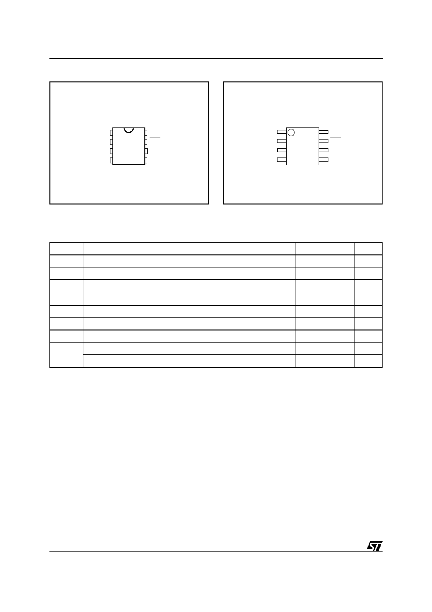
8
1
SO8 (M)
150mil Width
8
1
PSDIP8 (B)
0.25mm Frame
8
1
TSSOP8 (DW)
169 mil width
When writing data to the memory, it responds to the
8 bits received by asserting an acknowledge bit
during the 9th bit time. When data is read by the
bus master, it acknowledges the receipt of the data
bytes in the same way. Data transfers are termi-
nated with a STOP condition.
Power On Reset: V
CC
lock out write protect. In
order to prevent data corruption and inadvertent
write operations during power up, a Power On
Reset (POR) circuit is implemented. Until the V
CC
voltage has reached the POR threshold value, the
internal reset is active, all operations are disabled
and the device will not respond to any command.
In the same way, when V
CC
drops down from the
operating voltage to below the POR threshold
value, all operations are disabled and the device
will not respond to any command. A stable V
CC
must be applied before applying any logic signal.
SDA
VSS
SCL
WC
NC
NC
VCC
NC
AI01322
M2201
1
2
3
4
8
7
6
5
Figure 2A. DIP Pin Connections
1
AI01323
2
3
4
8
7
6
5
SDA
VSS
SCL
WC
NC
NC
VCC
NC
M2201
Figure 2B. SO and TSSOP Pin Connections
DESCRIPTION (cont'd)
Symbol
Parameter
Value
Unit
T
A
Ambient Operating Temperature
≠40 to 85
∞
C
T
STG
Storage Temperature
≠65 to 150
∞
C
T
LEAD
Lead Temperature, Soldering
(SO8 package)
(PSDIP8 package)
(TSSOP8 package)
40 sec
10 sec
t.b.c.
215
260
t.b.c.
∞
C
V
O
Output Voltage
≠0.6 to 6.5
V
V
I
Input Voltage
≠0.6 to 6.5
V
V
CC
Supply Voltage
≠0.3 to 6.5
V
V
ESD
Electrostatic Discharge Voltage (Human Body model)
(2)
4000
V
Electrostatic Discharge Voltage (Machine model)
(3)
500
V
Notes: 1. Except for the rating "Operating Temperature Range", stresses above those listed in the Table "Absolute Maximum Ratings"
may cause permanent damage to the device. These are stress ratings only and operation of the device at these or any other
conditions above those indicated in the Operating sections of this specification is not implied. Exposure to Absolute Maximum
Rating conditions for extended periods may affect device reliability. Refer also to the STMicroelectronics SURE Program and other
relevant quality documents.
2. MIL-STD-883C, 3015.7 (100pF, 1500
).
3. EIAJ IC-121 (Condition C) (200pF, 0
).
Table 2. Absolute Maximum Ratings
(1)
Warning: NC = Not Connected.
Warning: NC = Not Connected.
2/15
M2201

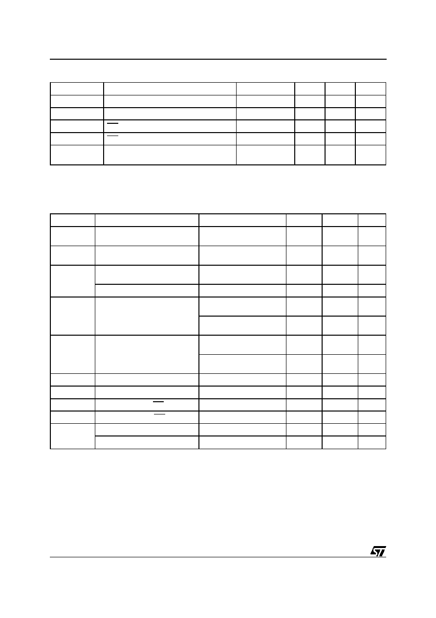
AI01100
VCC
CBUS
SDA
RL
MASTER
RL
SCL
CBUS
100
200
300
400
0
4
8
12
16
20
CBUS (pF)
R
L
max (k
)
VCC = 5V
Figure 3. Maximum R
L
Value versus Bus Capacitance (C
BUS
)
SIGNAL DESCRIPTIONS
Serial Clock (SCL). The SCL input pin is used to
synchronize all data in and out of the memory. A
resistor can be connected from the SCL line to V
CC
to act as a pull up (see Figure 3).
Serial Data (SDA). The SDA pin is bi-directional
and is used to transfer data in or out of the memory.
It is an open drain output that may be wire-OR'ed
with other open drain or open collector signals on
the bus. A resistor must be connected from the SDA
bus line to V
CC
to act as pull up (see Figure 3).
Write Control (WC). An hardware Write Control
feature (WC) is offered on pin 7. This feature is
usefull to protect the contents of the memory from
any erroneous erase/write cycle. The Write Control
signal is used to enable (WC = V
IH
) or disable (WC
= V
IL
) the internal write protection. When uncon-
nected, the WC input is internally read as V
IL
(WC
is disabled).
DEVICE OPERATION
The device that controls the data transfer is known
as the master. The master will always initiate a data
transfer and will provide the serial clock for syn-
chronisation. The M2201 is always a slave device
in all communications.
Start Condition. START is identified by a high to
low transition of the SDA line while the clock SCL
is stable in the high state. A START condition must
precede any command for data transfer. Except
during a programming cycle, the M2201 continu-
ously monitor the SDA and SCL signals for a
START condition and will not respond unless one
is given.
Stop Condition. STOP is identified by a low to high
transition of the SDA line while the clock SCL is
stable in the high state. A STOP condition termi-
nates communication between the M2201 and the
bus master. A STOP condition at the end of a Read
command forces the standby state. A STOP condi-
tion at the end of a Write command triggers the
internal EEPROM write cycle.
Acknowledge Bit (ACK). An acknowledge signal
is used to indicate a successfull data transfer. The
bus transmitter, either master or slave, will release
the SDA bus after sending 8 bits of data. During the
9th clock pulse period the receiver pulls the SDA
bus low to acknowledge the receipt of the 8 bits of
data.
Data Input. During data input the M2201 sample
the SDA bus signal on the rising edge of the clock
SCL. Note that for correct device operation the SDA
signal must be stable during the clock low to high
transition and the data must change ONLY when
the SCL line is low.
3/15
M2201
Symbol
Parameter
Test Condition
Min
Max
Unit
C
IN
Input Capacitance (SDA)
8
pF
C
IN
Input Capacitance (other pins)
6
pF
Z
WCL
(1)
WC Input Impedance
V
IN
0.3 V
CC
5
20
k
Z
WCH
(1)
WC Input Impedance
V
IN
0.7 V
CC
500
k
t
LP
(1)
Low-pass filter input time constant
(SDA and SCL)
100
ns
Note: 1. The results come from simulation, actual results may vary. These figures are not guaranteed.
Table 3. Input Parameters (T
A
= 25
∞
C, f = 100 kHz )
Symbol
Parameter
Test Condition
Min
Max
Unit
I
LI
Input Leakage Current
(SCL, SDA)
0V
V
IN
V
CC
±
2
µ
A
I
LO
Output Leakage Current
0V
V
OUT
V
CC
SDA in Hi-Z
±
2
µ
A
I
CC
Supply Current (M2201)
V
CC
= 5V; f
C
= 100kHz
(Rise/Fall time < 30ns)
2
mA
Supply Current (M2201V)
V
CC
= 2.7V; f
C
= 100kHz
1
mA
I
CC1
Supply Current (Standby)
(M2201)
V
IN
= V
SS
or V
CC
,
V
CC
= 5V
100
µ
A
V
IN
= V
SS
or V
CC
,
V
CC
= 5V, f
C
= 100kHz
300
µ
A
I
CC2
Supply Current (Standby)
(M2201V)
V
IN
= V
SS
or V
CC
,
V
CC
= 2.7V
5
µ
A
V
IN
= V
SS
or V
CC
,
V
CC
= 2.7V; f
C
= 100kHz
50
µ
A
V
IL
Input Low Voltage (SCL, SDA)
≠0.3
0.3 V
CC
V
V
IH
Input High Voltage (SCL, SDA)
0.7 V
CC
V
CC
+ 1
V
V
IL
Input Low Voltage (WC)
≠0.3
0.5
V
V
IH
Input High Voltage (WC)
V
CC
≠ 0.5
V
CC
+ 1
V
V
OL
Output Low Voltage (M2201)
I
OL
= 3mA, V
CC
= 5V
0.4
V
Output Low Voltage (M2201V)
I
OL
= 2mA, V
CC
= 2.7V
0.4
V
Table 4. DC Characteristics
(T
A
= 0 to 70
∞
C or ≠40 to 85
∞
C; V
CC
= 4.5V to 5.5V or 2.7V to 5.5V)
4/15
M2201
Symbol
Alt
Parameter
Min
Max
Unit
t
CH1CH2
t
R
Clock Rise Time
1
µ
s
t
CL1CL2
t
F
Clock Fall Time
300
ns
t
DH1DH2
t
R
Input Rise Time
1
µ
s
t
DL1DL1
t
F
Input Fall Time
300
ns
t
CHDX
(1)
t
SU:STA
Clock High to Input Transition
4.7
µ
s
t
CHCL
t
HIGH
Clock Pulse Width High
4
µ
s
t
DLCL
t
HD:STA
Input Low to Clock Low (START)
4
µ
s
t
CLDX
t
HD:DAT
Clock Low to Input Transition
0
µ
s
t
CLCH
t
LOW
Clock Pulse Width Low
4.7
µ
s
t
DXCX
t
SU:DAT
Input Transition to Clock Transition
250
ns
t
CHDH
t
SU:STO
Clock High to Input High (STOP)
4.7
µ
s
t
DHDL
t
BUF
Input High to Input Low (Bus Free)
4.7
µ
s
t
CLQV
(2)
t
AA
Clock Low to Next Data Out Valid
0.3
3.5
µ
s
t
CLQX
t
DH
Data Out Hold Time
300
ns
f
C
f
SCL
Clock Frequency
100
kHz
t
W
t
WR
Write Time
10
ms
Notes: 1. For a reSTART condition, or following a write cycle.
2. The minimum value delays the falling/rising edge of SDA away from SCL = 1 in order to avoid unwanted START and/or STOP
conditions.
Table 5. AC Characteristics
(T
A
= 0 to 70
∞
C or ≠40 to 85
∞
C; V
CC
= 4.5V to 5.5V or 2.7V to 5.5V)
Memory Addressing. To start communication be-
tween the bus master and the slave M2201, the
master must initiate a START condition. Following
this, the master sends onto the SDA bus line 8 bits
(MSB first) corresponding to the 7th bit byte-ad-
dress and a READ or WRITE bit. This 8th bit is set
to '1' for read and '0' for write operations. If a match
is found, the corresponding memory will acknow-
ledge the identification on the SDA bus during the
9th bit time.
Write Operations
Following a START condition the master sends the
byte address with the RW bit reset to '0'. The
memory acknowledges this and waits for a data
byte. Any write command with WC = 1 (during a
period of time from the START condition until the
end of the Byte Address) will not modify data and
will NOT be acknowledged on data bytes, as in
Figure 8.
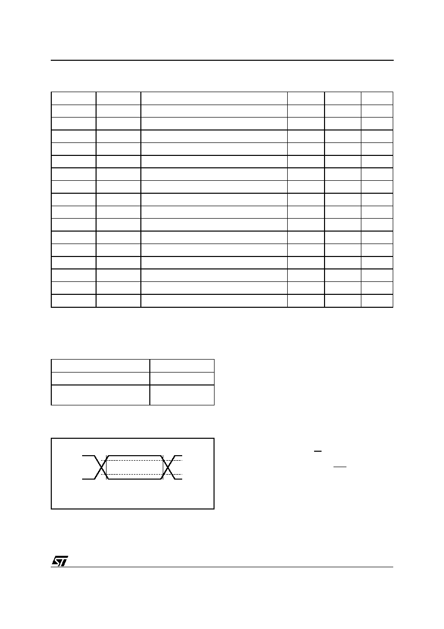
Input Rise and Fall Times
50ns
Input Pulse Voltages
0.2V
CC
to 0.8V
CC
Input and Output Timing Ref.
Voltages
0.3V
CC
to 0.7V
CC
Table 6. AC Measurement Conditions
AI00825
0.8VCC
0.2VCC
0.7VCC
0.3VCC
Figure 4. AC Testing Input Output Waveforms
5/15
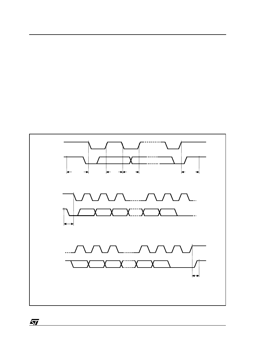
M2201

SCL
SDA IN
SCL
SDA OUT
SCL
SDA IN
tCHCL
tDLCL
tCHDX
START
CONDITION
tCLCH
tDXCX
tCLDX
SDA
INPUT
SDA
CHANGE
tCHDH
tDHDL
STOP &
BUS FREE
DATA VALID
tCLQV
tCLQX
DATA OUTPUT
tCHDH
STOP
CONDITION
tCHDX
START
CONDITION
WRITE CYCLE
tW
AI00795B
Figure 5. AC Waveforms
6/15
M2201
SCL
SDA
SCL
SDA
SDA
START
CONDITION
SDA
INPUT
SDA
CHANGE
AI00792
STOP
CONDITION
1
2
3
7
8
9
MSB
ACK
START
CONDITION
SCL
1
2
3
7
8
9
MSB
ACK
STOP
CONDITION
Figure 6. I
2
C Bus Protocol
Byte Write. In the Byte Write mode the master
sends one data byte, which is acknowledged by the
memory. The master then terminates the transfer
by generating a STOP condition.
Page Write. The Page Write mode allows up to 4
bytes to be written in a single write cycle, provided
that they are all located in the same 'row' in the
memory: that is the 5 most significant memory
address bits (A6-A2) are the same. The master
sends from one up to four bytes of data, which are
each acknowledged by the memory. After each
byte is transfered, the internal byte address counter
(2 least significant bits only) is incremented. The
transfer is terminated by the master generating a
STOP condition. Care must be taken to avoid ad-
dress counter 'roll-over' which could result in data
being overwritten.
It must be noticed that, for any write mode, the
generation by the master of the STOP condition
starts the internal memory program cycle. All inputs
are disabled until the completion of this cycle and
the memory will not respond to any request.
Minimizing System Delays by Polling On ACK.
During the internal write cycle, the memory discon-
nects itself from the bus in order to copy the data
from the internal latches to the memory cells. The
maximum value of the write time (t
W
) is given in the
AC Characteristics table, since the typical time is
shorter, the time seen by the system may be re-
7/15
M2201

WRITE Cycle
in Progress
AI01049
Next
Operation is
WRITE
START Condition
Byte Address
with RW = 0
ACK
Returned
YES
NO
YES
NO
ReSTART
STOP
Send
DATA BYTE
STOP
Figure 7. Write Cycle Polling using ACK
duced by an ACK polling sequence issued by the
master. The sequence is as follows:
≠ Initial condition: a Write is in progress (see Fig-
ure 7).
≠ Step 1: the Master issues a START condition
followed by a Device Select byte (1st byte of
the new instruction).
DEVICE OPERATION (cont'd)
≠ Step 2: if the memory is busy with the internal
write cycle, no ACK will be returned and the
master goes back to Step 1. If the memory
has terminated the internal write cycle, it will
respond with an ACK, indicating that the mem-
ory is ready to receive the second part of the
next instruction (the first byte of this instruc-
tion was already sent during Step 1).
8/15
M2201
ACK
NO ACK
STOP
START
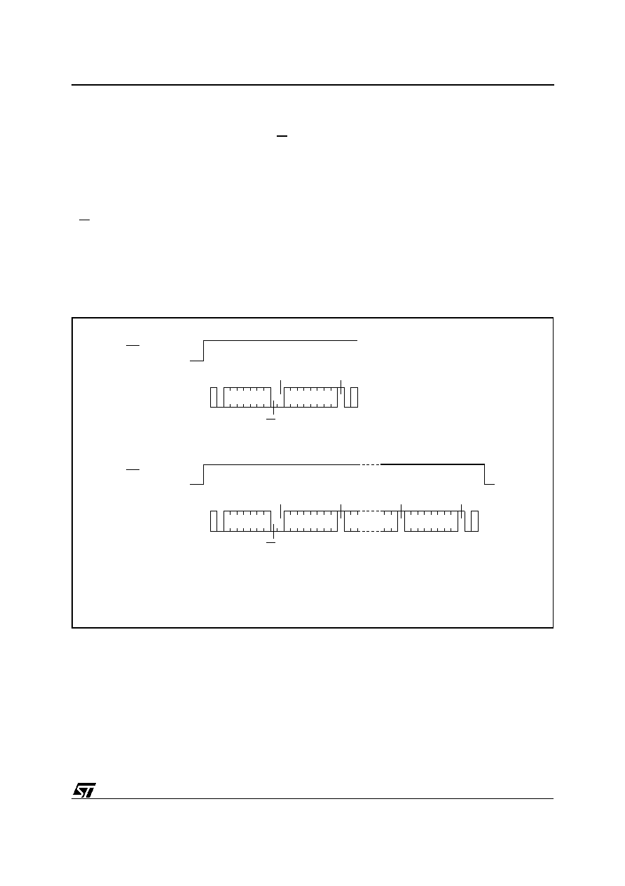
BYTE WRITE
R/W = 0
BYTE ADDR
DATA IN
WC
START
PAGE WRITE
BYTE ADDR
DATA IN 1
WC
AI01324
DATA IN 4
STOP
R/W = 0
ACK
NO ACK
NO ACK
NO ACK
Figure 8. Write Modes Sequences with Write Control = 1 (M2201 and M2201V)
Read Operation
Byte Read. The master sends a START condition
followed by seven bits of address and the RW bit
(set to '1'). The M2201 acknowledges it and outputs
the corresponding data byte. The read operation
is terminated by a STOP condition issued by the
master (instead of the ACK bit).
Sequential Read. The master sends a START
condition followed by seven bits of address and the
RW bit (set to '1'). The M2201 acknowledges it and
outputs the corresponding data byte. The master
does acknowledge this byte and reads the next
data byte (at address + 1). The read operation is
terminated by a STOP condition issued by the
master (instead of the ACK bit). The output data is
from consecutive byte addresses, with the internal
byte address counter automatically incremented
after each byte output. After a count of the last
memory address, the address counter will 'roll-
over to address '00' and the memory will continue
to output data.
Acknowledge in Read Mode. In all read modes
the M2201 waits for an acknowledge during the 9th
bit time. If the master does not pull the SDA line low
during this time, the M2201 terminates the data
transfer and switches to a standby state.
9/15
M2201

STOP
START
BYTE READ
BYTE ADDR
DATA OUT
START
SEQUENTIAL READ
BYTE ADDR
DATA OUT 1
AI01325
DATA OUT N
STOP
R/W = 1
ACK
ACK
ACK
NO ACK
NO ACK
ACK
R/W = 1
Figure 10. Read Modes Sequences
Byte-Address
STOP
START
BYTE WRITE
Data-In
START
PAGE WRITE
Data-In1
Data-In 2
Data-In 3
AI03128
STOP
Data-In N
ACK
ACK
R/W=0
ACK
ACK
ACK
R/W=0
ACK
ACK
Byte-Address
Figure 9. Write Modes Sequences (M2201 and M2201V)
10/15
M2201
ORDERING INFORMATION SCHEME
Devices are shipped from the factory with the memory content set at all "1's" (FFh).
For a list of available options (Operating Voltage, Package, etc...) or for further information please contact
the STMicroelectronics Sales Office nearest to you.
Operating Voltage
blank 4.5V to 5.5V
V
2.7V to 5.5V
Package
B
PSDIP8
0.25mm Frame
M
SO8
150mil Width
DW
TSSOP8
169mil width
Temperature Range
1
0 to 70
∞
C
6
≠40 to 85
∞
C
Option
TR
Tape & Reel
Packing
Example: M2201 V M 1 TR
11/15
M2201
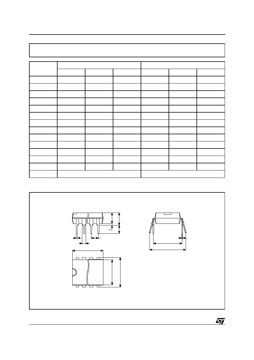
PSDIP-a
A2
A1
A
L
e1
D
E1
E
N
1
C
eA
eB
B1
B
Symb
mm
inches
Typ
Min
Max
Typ
Min
Max
A
3.90
5.90
0.154
0.232
A1
0.49
≠
0.019
≠
A2
3.30
5.30
0.130
0.209
B
0.36
0.56
0.014
0.022
B1
1.15
1.65
0.045
0.065
C
0.20
0.36
0.008
0.014
D
9.20
9.90
0.362
0.390
E
7.62
≠
≠
0.300
≠
≠
E1
6.00
6.70
0.236
0.264
e1
2.54
≠
≠
0.100
≠
≠
eA
7.80
≠
0.307
≠
eB
10.00
0.394
L
3.00
3.80
0.118
0.150
N
8
8
PSDIP8 - 8 pin Plastic Skinny DIP, 0.25mm lead frame
Drawing is not to scale.
12/15
M2201
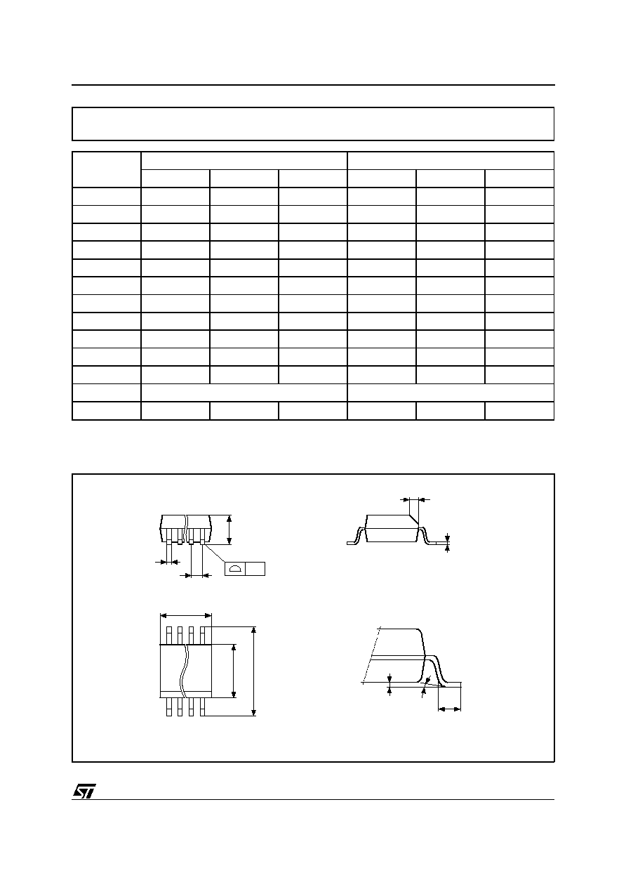
SO-a
E
N
CP
B
e
A
D
C
L
A1
1
H
h x 45∞
Symb
mm
inches
Typ
Min
Max
Typ
Min
Max
A
1.35
1.75
0.053
0.069
A1
0.10
0.25
0.004
0.010
B
0.33
0.51
0.013
0.020
C
0.19
0.25
0.007
0.010
D
4.80
5.00
0.189
0.197
E
3.80
4.00
0.150
0.157
e
1.27
≠
≠
0.050
≠
≠
H
5.80
6.20
0.228
0.244
h
0.25
0.50
0.010
0.020
L
0.40
0.90
0.016
0.035
0
∞
8
∞
0
∞
8
∞
N
8
8
CP
0.10
0.004
Drawing is not to scale.
SO8 - 8 lead Plastic Small Outline, 150 mils body width
13/15
M2201

TSSOP
1
N
CP
N/2
DIE
C
L
A1
E
E1
D
A2
A
e
B
Symb
mm
inches
Typ
Min
Max
Typ
Min
Max
A
1.10
0.043
A1
0.05
0.15
0.002
0.006
A2
0.85
0.95
0.033
0.037
B
0.19
0.30
0.007
0.012
C
0.09
0.20
0.004
0.008
D
2.90
3.10
0.114
0.122
E
6.25
6.50
0.246
0.256
E1
4.30
4.50
0.169
0.177
e
0.65
≠
≠
0.026
≠
≠
L
0.50
0.70
0.020
0.028
0
∞
8
∞
0
∞
8
∞
N
8
8
CP
0.08
0.003
Drawing is not to scale.
TSSOP8 - 8 lead Plastic Thin Shrink Small Outline, 169 mils body width
14/15
M2201

Information furnished is believed to be accurate and reliable. However, STMicroelectronics assumes no responsibility for the consequences
of use of such information nor for any infringement of patents or other rights of third parties which may result from its use. No license is granted
by implication or otherwise under any patent or patent rights of STMicroelectronics. Specifications mentioned in this publication are subject to
change without notice. This publication supersedes and replaces all information previously supplied. STMicroelectronics products are not
authorized for use as critical components in life support devices or systems without express written approval of STMicroelectronics.
The ST logo is a registered trademark of STMicroelectronics
© 1999 STMicroelectronics - All Rights Reserved
STMicroelectronics GROUP OF COMPANIES
Australia - Brazil - China - Finland - France - Germany - Hong Kong - India - Italy - Japan - Malaysia - Malta -
Morocco - Singapore - Spain - Sweden - Switzerland - United Kingdom - U.S.A.
http://www.st.com
15/15
M2201