 | –≠–ª–µ–∫—Ç—Ä–æ–Ω–Ω—ã–π –∫–æ–º–ø–æ–Ω–µ–Ω—Ç: M22100 | –°–∫–∞—á–∞—Ç—å:  PDF PDF  ZIP ZIP |
M22100
September 1988
4 X 4 CROSSPOINT SWITCH WITH CONTROL MEMORY
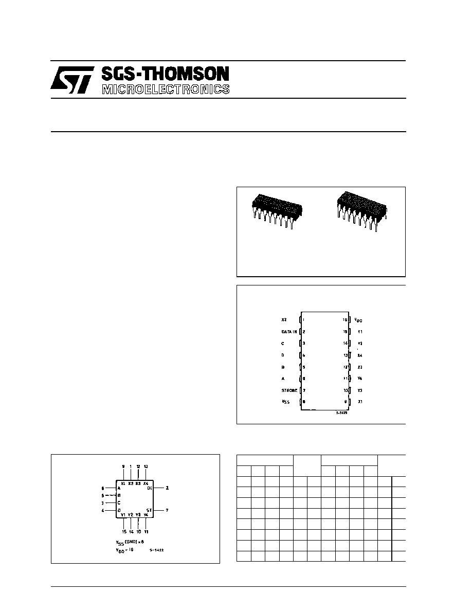
EY
(Plastic Package)
ORDER CODES :
M22100 B1
M22100 F1
F
(Ceramic Package)
FUNCTIONAL DIAGRAM
.
LOW ON RESISTANCE ≠ 75
TYP. AT
V
DD
= 12 V
.
"BUILT-IN" CONTROL LATCHES
.
LARGE ANALOG SIGNAL CAPABILITY
±
V
DD
/2
.
TRANSMITS SIGNALS UP TO 10 MHz
.
MATCHED SWITCH CHARACTERISTICS
R
ON
= 18
TYP. AT V
DD ≠
V
SS
= 12 V.
.
HIGH LINEARITY : ≠ 0.5 % DISTORTION (typ.)
AT f = 1 KHz, V
IN
= 5 V PEAK TO PEAK, V
DD
-
V
SS
= 10 V, R
L
= 10 K
.
STANDARD COS/MOS NOISE IMMUNITY
.
100 % TESTED FOR QUIESCENT CURRENT
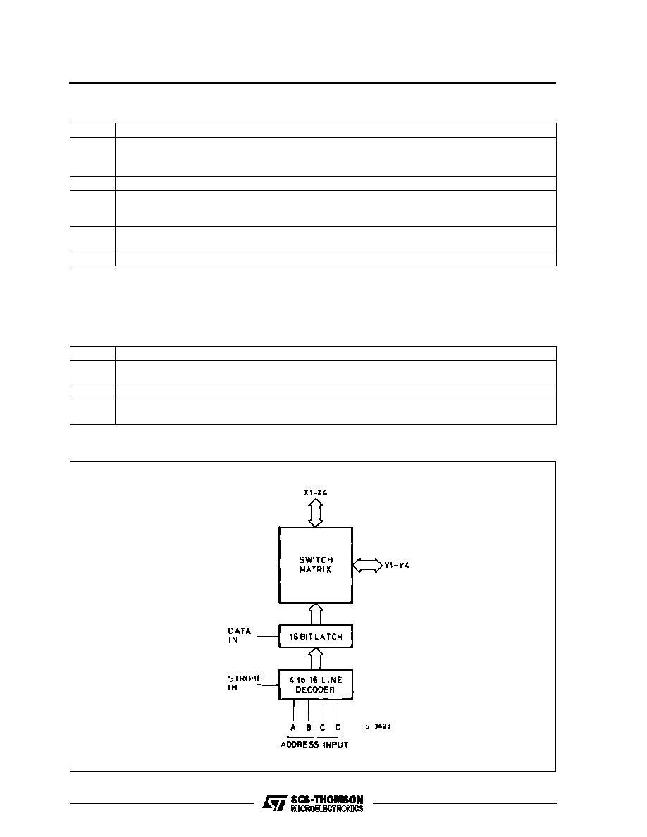
The M22100 combines a 4 x 4 array of crosspoints
(transmission gates) with a 4-line-to-16-line decoder
and 16 latch circuits. Any one of the sixteen trans-
mission gates (crosspoints) can be selected by ap-
plying the appropriate four line address. The
selected transmission gate can be turned on or off
by applying a logical one or zero, respectively, to the
data input and strobing the strobe input to a logical
one. Any number of the transmission gates can be
ON simultaneously.
When the required operating power is applied to the
22100, the states of the 16 switches are indetermi-
nate.
Therefore, all switches must be turned off by putting
the strobe high and data-in-low, and then address-
ing all switches in succession.
DESCRIPTION
TRUTH TABLE
Address
Select
Address
Select
A
B
C
D
A
B
C
D
0
0
0
0
X1 Y1
0
0
0
1
X1 Y3
1
0
0
0
X2 Y1
1
0
0
1
X2 Y3
0
1
0
0
X3 Y1
0
1
0
1
X3 Y3
1
1
0
0
X4 Y1
1
1
0
1
X4 Y3
0
0
1
0
X1 Y2
0
0
1
1
X1 Y4
1
0
1
0
X2 Y2
1
0
1
1
X2 Y4
0
1
1
0
X3 Y2
0
1
1
1
X3 Y4
1
1
1
0
X4 Y2
1
1
1
1
X4 Y4
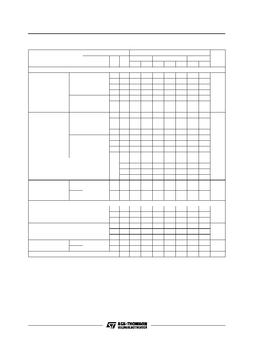
PIN CONNECTIONS
1/13
ABSOLUTE MAXIMUM RATING
Symbol
Parameter
Value
Unit
V
DD
*
Supply Voltage: Ceramic Types
Plastic Types
-0.5 to +20
-0.5 to +18
V
V
V
i
Input Voltage
-0.5 to V
DD
+ 0.5
V
I
I
DC Input Current (any one input)
±
10
mA
P
tot
Total Power Dissipation (per package)
Dissipation per Output Transistor
for Top = Full Package Temperature Range
200
100
mW
mW
T
op
Operating Temperature: Ceramic Types
Plastic Types
-55 to +125
-40 to +85
o
C
o
C
T
stg
Storage Temperature
-65 to +150
o
C
Stresses above those listed under "Absolute Maximum Ratings" may cause permanent damage to the device. This is a stress ratingonly and functional
operation of the device at these or any other conditions above those indicated in the operational sections of this specification is not implied. Exposure
to absolute maximum rating conditions for external periods may affect device reliability.
* All voltage values are referred to V
SS
pin voltage.
RECOMMENDED OPERATING CONDITIONS
Symbol
Parameter
Value
Unit
V
DD
Supply Voltage: Ceramic Types
Plastic Types
3 to 18
3 to 15
V
V
V
I
Input Voltage
0 to V
DD
V
T
op
Operating Temperature: Ceramic Types
Plastic Types
-55 to +125
-40 to +85
o
C
o
C
LOGIC DIAGRAM
M22100
2/13
STATIC ELECTRICAL CHARACTERISTICS (over recommended operating conditions)
Symbol
Parameter
Test Conditios
Value
Unit
V
I
(V)
V
DD
(V)
T
LOW
*
25
o
C
T
HIGH
*
Min.
Max.
Min.
Typ.
Max.
Min.
Max.
CROSSPOINT
I
L
Quiescent
Supply
Current
F1
5
0.04
5
150
µ
A
10
0.04
10
300
15
0.04
20
600
20
0.08
100
3000
B1
5
0.04
20
150
10
0.04
40
300
15
0.04
80
600
R
ON
On
Resistance
F1
Any Switch
5
450
225
1250
1625
10
135
85
180
230
12
100
75
135
175
15
70
65
95
125
B1
V
IS
= 0 to V
DD
5
1000
225
1250
1440
10
145
85
180
205
12
110
75
135
155
15
75
65
95
110
ON
Resistance
R
ON
(Between any two
channels)
5
35
10
20
12
18
15
15
OFF
Channel
Leakage
Current
F1
All Switch
OFF
0/18
18
±
0.1
±
10
-3
±
0.1
∑
±
1
µ
A
B1
0/15
15
±
0.3
±
10
-3
±
0.3
±
1
CONTROL
V
IL
Input Low
Voltage
OFF Switch
I
L
< 0.2
µ
A
5
1.5
1.5
1.5
V
10
3
3
3
15
4
4
4
V
IH
Input High
Voltage
ON Switch
see R
ON
Characteristics
5
3.5
3.5
3.5
V
10
7
7
7
15
11
11
11
I
I
Input
Current
F1
Any Control
Input
0/18
18
±
0.1
±
10
-5
±
0.1
∑
±
1
µ
A
B1
0/15
15
±
0.3
±
10
-5
±
0.3
±
1
C
I
Input Capacitance
Any Input
5
7.5
pF
∑
Determined by minimum feasible leakage measurement for automatic testing
* T
LOW
= -55
o
C for HCC device: -40
o
C for HCF device.
* T
HIGH
= +125
o
C for HCC device: +85
o
C for HCF device.
The Noise Margin for both "1" and "0" level is: 1V min. with V
DD
= 5 V, 2 V min. with V
DD
= 10 V, 2.5 V min. with V
DD
= 15 V
M22100
3/13
DYNAMIC ELECTRICAL CHARACTERISTICS (T
amb
= 25
o
C, C
L
= 50 pF, all input rise and fall
times= 20 ns)
Symbol
Parameter
Test Conditions
Value
Unit
f
i
(KHz)
R
L
(KW)
V
IS
∑
(V)
V
DD
(V)
Min.
Typ.
Max.
CROSSPOINT
t
PHL
t
PLH
Propagation Delay Time
Address or Strobe
Inputs to Output
10
5
5
30
60
ns
10
10
15
30
15
15
10
20
Frequency Response
(Any Switch ON)
1
1
5
10
40
MHz
Sine Wave Input
20
Log
V
OS
V
IS
= -
3
dB
Sine Wave Distortion
1
1
5
10
0.5
%
Feedthrough
(All Switches OFF)
1.6
1
5
10
80
dB
Sine Wave Input
Frequency for Signal
Crosstalk
Attenuation of 40 dB
1
10
10
1.5
MHz
Sine Wave Input
Frequency for Signal
Crosstalk
Attenuation of 110 dB
1
10
10
0.1
KHz
Sine Wave Input
C
Capacitance
Xn to Ground
Yn to Ground
Feedthrough
5-15
18
30
0.4
pF
CONTROLS
t
PHZ
Propagation Delay Time
Strobe to Output (Switch
Turn-ON to High Level)
R
L
= 1 K
C
L
= 50 pF
t
r
, t
f
= 20 ns
See Figure 1
5
500
1000
ns
10
230
460
15
145
290
t
PZH
Propagation Delay Time
Data-In to Output (Switch
Turn-ON to High Level)
See Figure 2
5
500
1000
ns
10
220
440
15
135
270
t
PZH
Propagation Delay Time
Address to Output (Switch
Turn-ON to High Level)
See Figure 3
5
480
960
ns
10
225
450
15
150
300
t
PHZ
Propagation Delay Time
Strobe to Output (Switch
Turn-OFF)
See Figure 1
5
450
900
ns
10
200
400
15
165
330
t
PZL
Propagation Delay Time
Data-In to Output (Switch
Turn-ON to Low Level)
See Figure 2
5
500
1000
ns
10
220
440
15
135
270
t
PHZ
Propagation Delay Time
Address to Output
(Switch Turn-OFF)
See Figure 3
5
425
850
ns
10
190
380
15
145
290
t
setup
Setup Time Data-In to
Strobe, Address
5
200
400
ns
10
80
160
15
50
100
∑
Peak to peak voltage symmetrical about V
DD
/2
M22100
4/13
DYNAMIC ELECTRICAL CHARACTERISTICS (continued)
Symbol
Parameter
Test Conditions
Value
Unit
f
i
(KHz)
R
L
(KW)
V
IS
∑
(V)
V
DD
(V)
Min.
Typ.
Max.
CONTROLS (continued)
t
hold
Hold Time Data-In to
Strobe, Address
R
L
= 1 K
C
L
= 50 pF
t
r
, t
f
= 20 ns
5
180
ns
10
110
15
35
f
Switching Frequency
5
0.6
1.2
MHz
10
1.6
3.2
15
2.5
5
t
W
Strobe Pulse Width
5
300
600
ns
10
120
240
15
90
180
Control Crosstalk
Data-In, Address, or
Storbe to Output
10
10
10
75
mV
(peak)
∑
Peak to peak volatge symmetrical about V
DD
/2
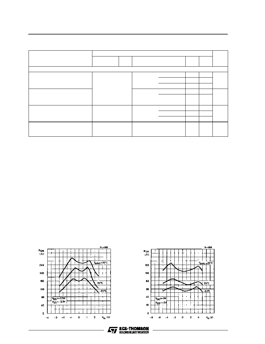
Typical ON Resistance vs. Input Signal Voltage at
V
DD
= ≠ V
SS
= 2.5 V.
Typical ON Resistance vs. Input Signal Voltage at
V
DD
= ≠ V
SS
= 5 V.
M22100
5/13
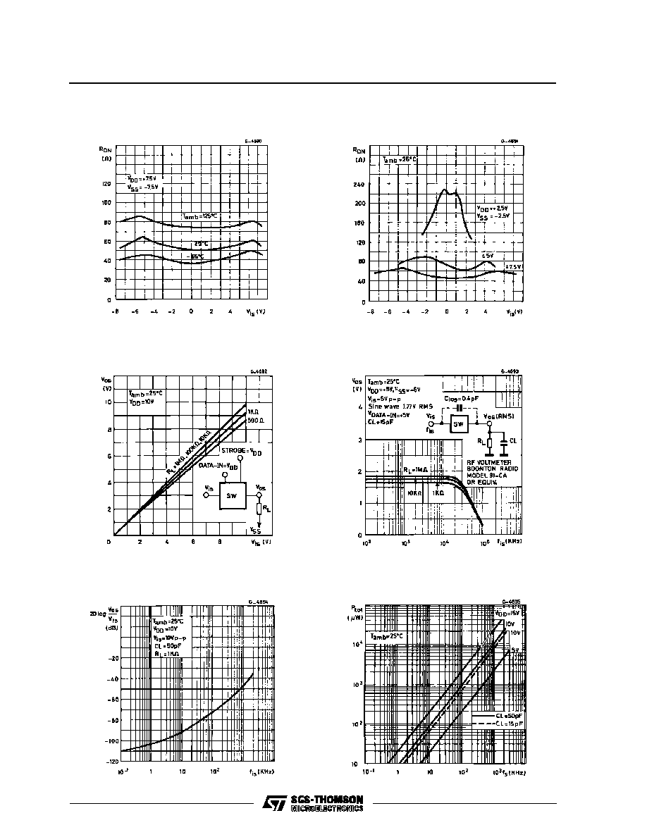
Typical ON Resistance vs. Input Signal Voltage at
V
DD
= ≠ V
SS
= 7.5 V.
Typical ON Resistance vs.. Input Signal Voltage
at T
amb
= 25
∞
C.
Typical Swich ON Transfert Characteristics
(1 of 16 switches).
Typical Swich ON Frequency Response
Characteristics.
Typical Crosstalk Between switches vs. Signal
Frequency.
Typical Dynamic Power Dissipation vs. Switching
Frequency..
M22100
6/13
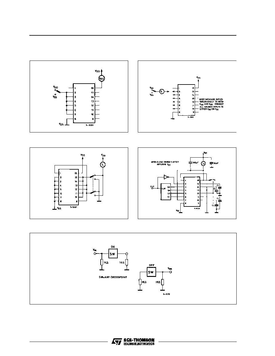
TEST CIRCUITS
Quiescent Current.
Input Current.
Off Switch Input or Output Leakage Current.
Dynamic Power Dissipation.
Croostalk Between Switch Circuits in the Same Package.
M22100
7/13
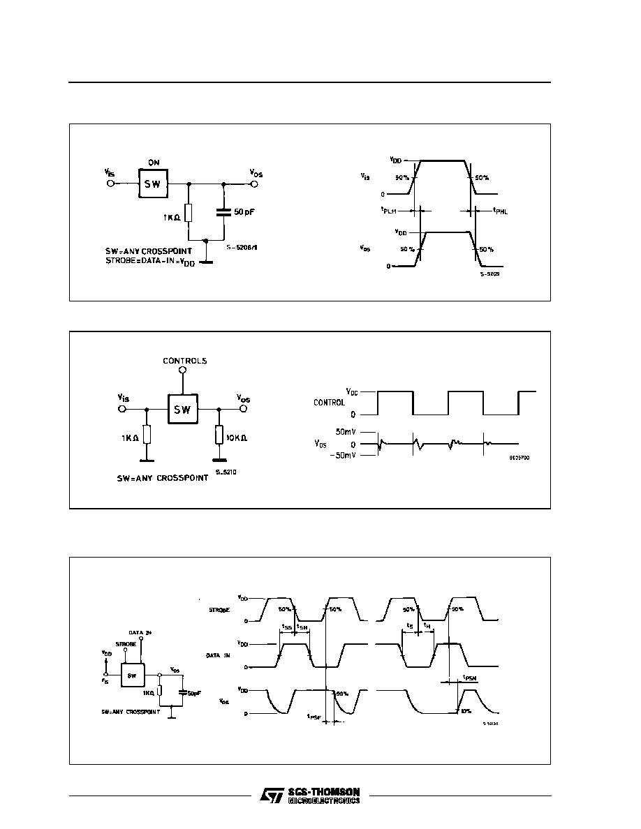
Propagation Delay Time and Waveforms (signal input to signal output, switch ON).
Waveforms for Crosstalk (control input to signal output).
Figure 1 : Propagation Delay Time and Waveforms (strobe to signal output, switch Turn-ON or Turn-
OFF).
M22100
8/13
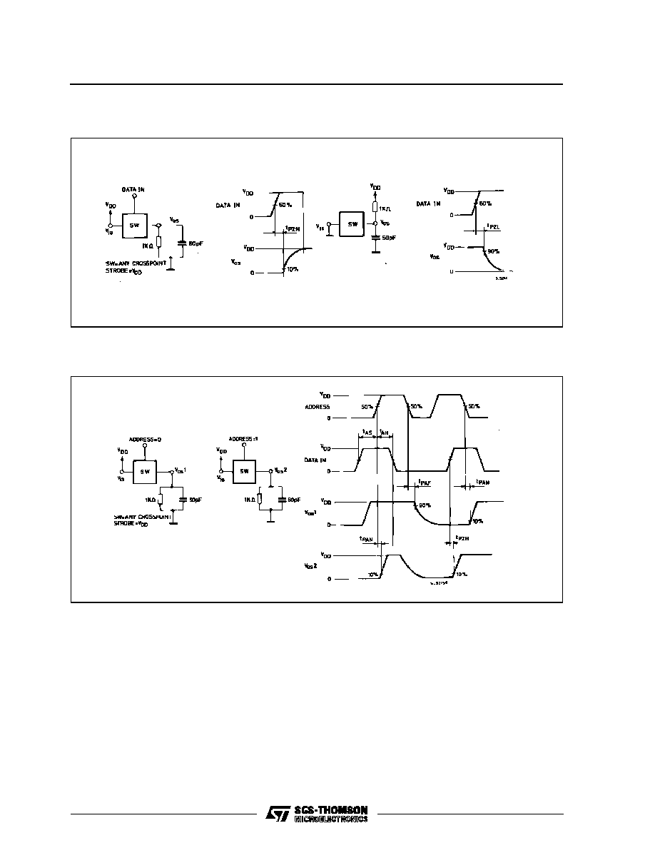
Figure 2 : Propagation Delay Time and Waveforms (data-in to signal output, switch Turn-ON to high or
low level).
Figure 3 : Propagation Delay Time and Waveforms (address to signal output switch Turn-ON or Turn-
OFF).
M22100
9/13
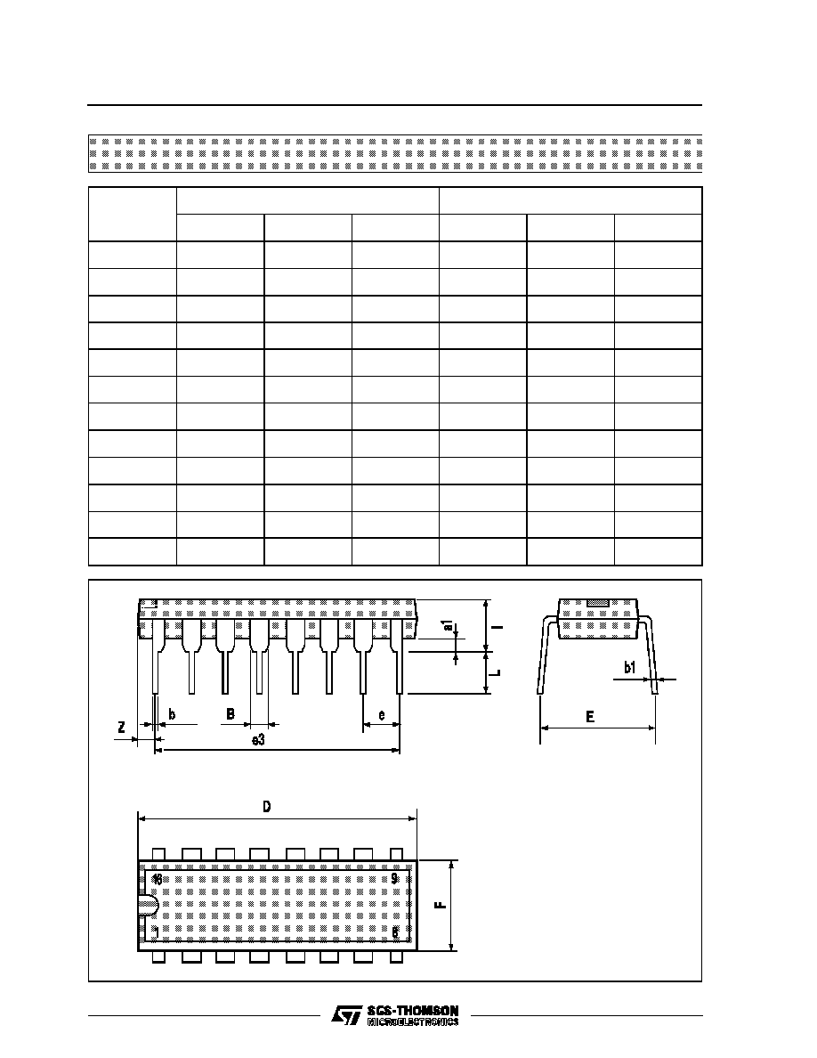
Plastic DIP16 (0.25) MECHANICAL DATA
DIM.
mm
inch
MIN.
TYP.
MAX.
MIN.
TYP.
MAX.
a1
0.51
0.020
B
0.77
1.65
0.030
0.065
b
0.5
0.020
b1
0.25
0.010
D
20
0.787
E
8.5
0.335
e
2.54
0.100
e3
17.78
0.700
F
7.1
0.280
I
5.1
0.201
L
3.3
0.130
Z
1.27
0.050
P001C
M22100
10/13
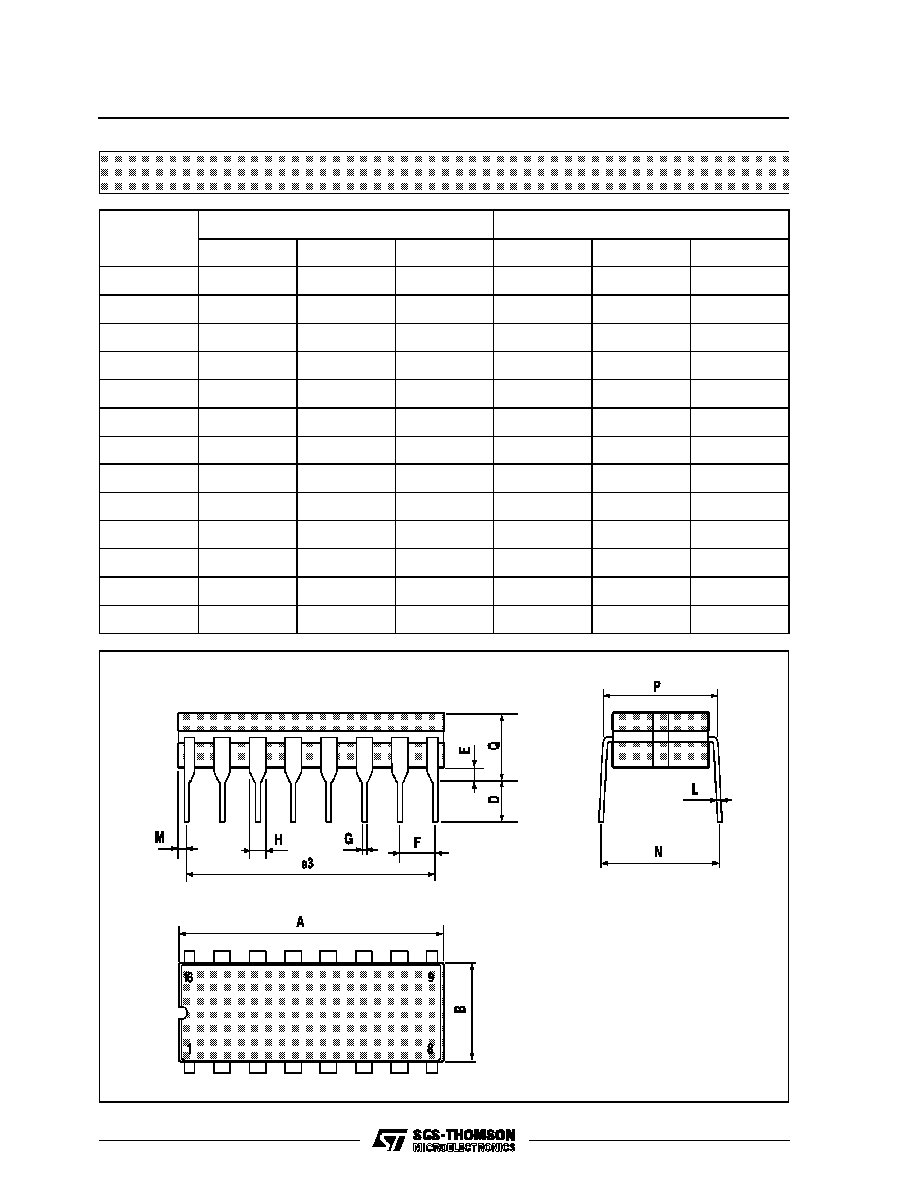
Ceramic DIP16/1 MECHANICAL DATA
DIM.
mm
inch
MIN.
TYP.
MAX.
MIN.
TYP.
MAX.
A
20
0.787
B
7
0.276
D
3.3
0.130
E
0.38
0.015
e3
17.78
0.700
F
2.29
2.79
0.090
0.110
G
0.4
0.55
0.016
0.022
H
1.17
1.52
0.046
0.060
L
0.22
0.31
0.009
0.012
M
0.51
1.27
0.020
0.050
N
10.3
0.406
P
7.8
8.05
0.307
0.317
Q
5.08
0.200
P053D
M22100
11/13
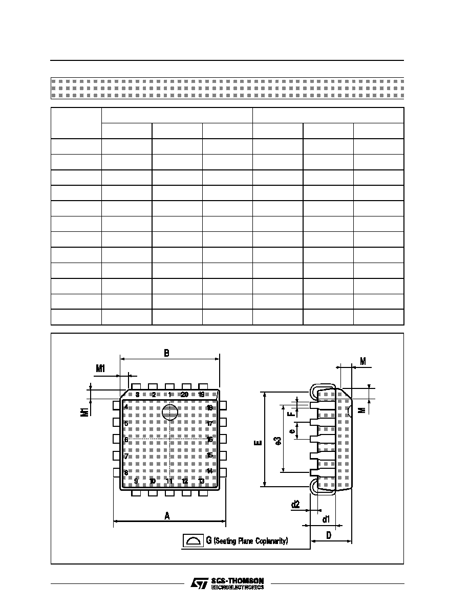
PLCC20 MECHANICAL DATA
DIM.
mm
inch
MIN.
TYP.
MAX.
MIN.
TYP.
MAX.
A
9.78
10.03
0.385
0.395
B
8.89
9.04
0.350
0.356
D
4.2
4.57
0.165
0.180
d1
2.54
0.100
d2
0.56
0.022
E
7.37
8.38
0.290
0.330
e
1.27
0.050
e3
5.08
0.200
F
0.38
0.015
G
0.101
0.004
M
1.27
0.050
M1
1.14
0.045
P027A
M22100
12/13

Information furnished is believed to be accurate and reliable. However, SGS-THOMSON Microelectronics assumes no responsability for the
consequences of use of such information nor for any infringement of patents or other rights of third parties which may results from its use. No
license is granted by implication or otherwise under any patent or patent rights of SGS-THOMSON Microelectronics. Specifications mentioned
in this publication are subject to change without notice. This publication supersedes and replaces all information previously supplied.
SGS-THOMSON Microelectronics products are not authorized for use as critical components in life support devices or systems without express
written approval of SGS-THOMSON Microelectonics.
©
1994 SGS-THOMSON Microelectronics - All Rights Reserved
SGS-THOMSON Microelectronics GROUP OF COMPANIES
Australia - Brazil - France - Germany - Hong Kong - Italy - Japan - Korea - Malaysia - Malta - Morocco - The Netherlands -
Singapore - Spain - Sweden - Switzerland - Taiwan - Thailand - United Kingdom - U.S.A
M22100
13/13