 | –≠–ª–µ–∫—Ç—Ä–æ–Ω–Ω—ã–π –∫–æ–º–ø–æ–Ω–µ–Ω—Ç: M22102B1 | –°–∫–∞—á–∞—Ç—å:  PDF PDF  ZIP ZIP |
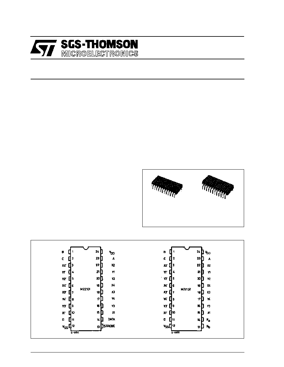
M22101
M22102
September 1988
WITH CONTROL MEMORY
4 X 4 X 2 CROSSPOINT SWITCHES
B1
(Plastic Package)
ORDER CODES :
M22XXX B1
M22XXX F1
F1
(Ceramic Package)
PIN CONNECTIONS
.
LOW ON RESISTANCE ≠ 75
TYP AT
V
DD
= 12 V
.
"BUILT-IN" LATCHED INPUTS
.
LARGE ANALOG SIGNAL CAPACITY
±
V
DD
/2
.
10 MHz SWITCH BANDWITH
.
MATCHED SWITCH CHARACTERISTICS
.
RON = 8
TYP, AT V
DD
= 12 V
.
HIGH LINEARITY ≠ 0.25 % DISTORTION TYP,
AT f = 1 kHz, V
IN
= 5 V, V
DD
- V
SS
= 10 V AND
RI = 1
.
STANDARD CMOS NOISE IMMUNITY
The M22101 and M22102 crosspoint switches con-
sist of 4 x 4 x 2 arrays of crosspoints (transmission
gates), 4-line to 16-line decoders, and 16 latch cir-
cuits. Any one of the sixteen crosspoint pairs can be
selected by applying the appropriate four-line ad-
dress and any number of crosspoint pairs can be ON
simultaneously. Corresponding crosspoints in each
array are turned on and OFF simultaneously, also.
In the M22101, the selected crosspoint pair can be
turned on or off by applying a logical ONE or ZERO,
respectively, to the data input, and applying a ONE
to the strobe input. When the device is "power-up",
the state of the 16 switches is indeterminate.
Therefore all switches must be turned off by putting
the strobe hight, data-in-low, and the addressing all
switches in succession.
The selected pair of crosspoints in the M22102 is
turned on by applying a logical ONE to the K
a
(set)
input while a logical ZERO is on the K
b
(reset) input,
and turned off by applying a logical ONE to the K
b
input while a logical ZERO is on the K
a
input. In this
respect the control latches of the M22102 are similar
to SET/RESET flip-flops. They differ, however, in
that the simultaneous application of ONEs to the K
a
and K
b
inputs turns off (resets) all crosspoints. All
crosspoints in both devices must be turned off as
V
DD
is applied.
DESCRIPTION
1/8

ABSOLUTE MAXIMUM RATING
Symbol
Parameter
Value
Unit
V
DD
Supply Voltage: Ceramic Type
Plastic Type
-0.5 to +20
-0.5 to +18
V
V
V
i
Input Voltage
-0.5 to V
DD
+ 0.5
V
I
I
DC Input Current (any one input)
±
10
mA
P
tot
Total Power Dissipation (per package)
Dissipation per Output Transistor
for Top = Full Package Temperature Range
200
100
mW
mW
T
op
Operating Temperature: Ceramic Type
Plastic Type
-55 to +125
-40 to +85
o
C
o
C
T
stg
Storage Temperature
-65 to +150
o
C
Stresses above those listed under "Absolute Maximum Ratings" may cause permanent damage to the device. This is a stress ratingonly and functional
operation of the device at these or any other conditions above those indicated in the operational sections of this specification is not implied. Exposure
to absolute maximum rating conditions for external periods may affect device reliability.
RECOMMENDED OPERATING CONDITIONS
Symbol
Parameter
Value
Unit
V
DD
Supply Voltage: Ceramic Type
Plastic Type
3 to 18
3 to 15
V
V
V
I
Input Voltage
0 to V
DD
V
T
op
Operating Temperature: Ceramic Type
Plastic Type
-55 to +125
-40 to +85
o
C
o
C
CONTROL TRUTH TABLE FOR M22101
Function
Address
Strobe
Data
Select
A
B
C
D
Switch-on
1
1
1
1
1
1
(X4 Y4) & (X4' Y4')
Switch-off
1
1
1
1
1
0
(X4 Y4) & (X4' Y4')
No Change
X
X
X
X
0
X
X X X X
Note: 1 = High, 0 = Low, X = Don't Care
CONTROL TRUTH TABLE FOR M22102
Function
Address
Strobe
Data
Select
A
B
C
D
Switch-on
1
1
1
1
1
0
(X4 Y4) & (X4' Y4')
Switch-off
1
1
1
1
0
1
(X4 Y4) & (X4' Y4')
All Switch-off
X
X
X
X
1
1
All
No Change
X
X
X
X
0
0
X X X X
Note: 1 = High, 0 = Low, X = Don't Care
M22101/M22102
2/8

FUNCTIONAL AND BLOCK DIAGRAM
DECODER TRUTH TABLE
Address
Select
Address
Select
A
B
C
D
A
B
C
D
0
0
0
0
X1 Y1
X1' Y1'
0
0
0
1
X1 Y3
X1' Y3'
1
0
0
0
X2 Y1
X2' Y1'
1
0
0
1
X2 Y3
X2' Y3'
0
1
0
0
X3 Y1
X3' Y1'
0
1
0
1
X3 Y3
X3' Y3'
1
1
0
0
X4 Y1
X4' Y1'
1
1
0
1
X4 Y3
X4' Y3'
0
0
1
0
X1 Y2
X1' Y2'
0
0
1
1
X1 Y4
X1' Y4'
1
0
1
0
X2 Y2
X2' Y2'
1
0
1
1
X2 Y4
X2' Y4'
0
1
1
0
X3 Y2
X3' Y2'
0
1
1
1
X3 Y4
X3' Y4'
1
1
1
0
X4 Y2
X4' Y2'
1
1
1
1
X4 Y4
X4' Y4'
M22101/M22102
3/8

STATIC ELECTRICAL CHARACTERISTICS (over recommended operating conditions)
Symbol
Parameter
Test Conditios
Value
Unit
V
I
(V)
V
DD
(V)
T
LOW
*
25
o
C
T
HIGH
*
Min.
Max.
Min.
Typ.
Max.
Min.
Max.
CROSSPOINT
I
L
Quiescent
Supply
Current
F1
5
0.04
5
150
µ
A
10
0.04
10
300
15
0.04
20
600
20
0.08
100
3000
B1
5
0.04
20
150
10
0.04
40
300
15
0.04
80
600
R
ON
On
Resistance
F1
Any Switch
5
450
225
1250
1625
10
135
85
180
230
12
100
75
135
175
15
70
65
95
125
B1
V
IS
= 0 to V
DD
5
1000
225
1250
1440
10
145
85
180
205
12
110
75
135
155
15
75
65
95
110
ON
Resistance
R
ON
(Between any two
channels)
5
35
10
20
12
18
15
15
OFF
Channel
Leakage
Current
F1
All Switch
OFF
0/18
18
±
0.1
±
10
-3
±
0.1
∑
±
1
µ
A
B1
0/15
15
±
0.3
±
10
-3
±
0.3
±
1
CONTROL
V
IL
Input Low
Voltage
OFF Switch
I
L
< 0.2
µ
A
5
1.5
1.5
1.5
V
10
3
3
3
15
4
4
4
V
IH
Input High
Voltage
ON Switch
see R
ON
Characteristics
5
3.5
3.5
3.5
V
10
7
7
7
15
11
11
11
I
I
Input
Current
F1
Any Control
Input
0/18
18
±
0.1
±
10
-5
±
0.1
±
1
µ
A
B1
0/15
15
±
0.3
±
10
-5
±
0.3
±
1
C
I
Input Capacitance
Any Input
5
7.5
pF
∑
Determined by minimum feasible leakage measurement for automatic testing
* T
LOW
= -55
o
C for HCC device: -40
o
C for HCF device.
* T
HIGH
= +125
o
C for HCC device: +85
o
C for HCF device.
The Noise Margin for both "1" and "0" level is: 1V min. with V
DD
= 5 V, 2 V min. with V
DD
= 10 V, 2.5 V min. with V
DD
= 15 V
M22101/M22102
4/8
DYNAMIC ELECTRICAL CHARACTERISTICS (T
amb
= 25
o
C, C
L
= 50 pF, R
L
= 200 K
,
typical temperature coefficent for all V
DD
values is 03 %/
o
C, all input rise and fall times= 20 ns)
Symbol
Parameter
Test Conditions
Value
Unit
V
DD
(V)
Min.
Typ.
Max.
t
PHL
t
PLH
Propagation Delay Time Address or Strobe
Inputs to Output
R
L
= 10 K
C
L
= 50 pF
12
200
ns
t
PHL
t
PLH
Propagation Delay Time Across Crosspoint
20
ns
Minimum Strobe Pulse Width
80
ns
M22101/M22102
5/8
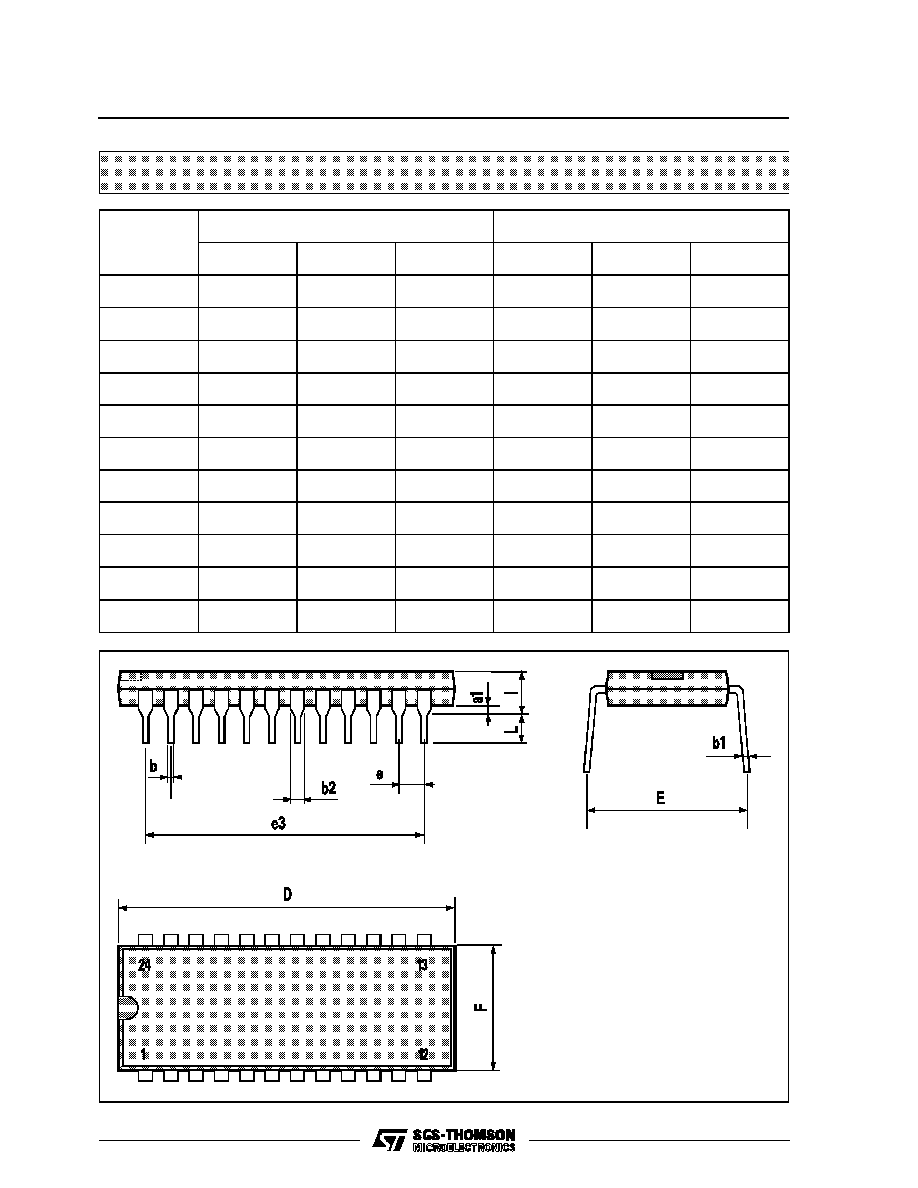
Plastic DIP24 (0.25) MECHANICAL DATA
DIM.
mm
inch
MIN.
TYP.
MAX.
MIN.
TYP.
MAX.
a1
0.63
0.025
b
0.45
0.018
b1
0.23
0.31
0.009
0.012
b2
1.27
0.050
D
32.2
1.268
E
15.2
16.68
0.598
0.657
e
2.54
0.100
e3
27.94
1.100
F
14.1
0.555
I
4.445
0.175
L
3.3
0.130
P043A
M22101/M22102
6/8
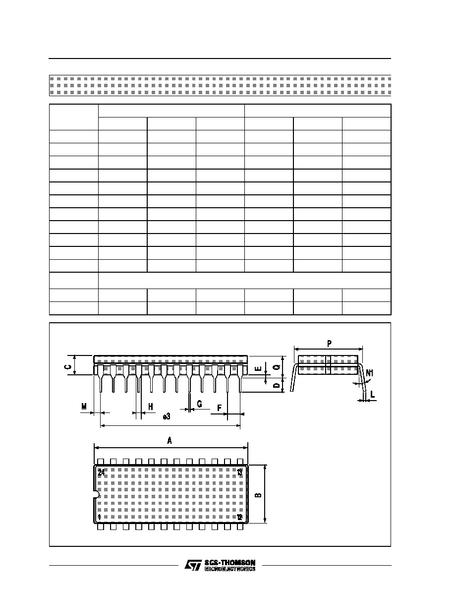
Ceramic DIP24 MECHANICAL DATA
DIM.
mm
inch
MIN.
TYP.
MAX.
MIN.
TYP.
MAX.
A
32.3
1.272
B
13.05
13.36
0.514
0.526
C
3.9
5.08
0.154
0.200
D
3
0.118
E
0.5
1.78
0.020
0.070
e3
27.94
1.100
F
2.29
2.79
0.090
0.110
G
0.4
0.55
0.016
0.022
I
1.17
1.52
0.046
0.060
L
0.22
0.31
0.009
0.012
M
1.52
2.49
0.060
0.098
N1
4
∞
(min.), 15
∞
(max.)
P
15.4
15.8
0.606
0.622
Q
5.71
0.225
P058C
M22101/M22102
7/8

Information furnished is believed to be accurate and reliable. However, SGS-THOMSON Microelectronics assumes no responsability for the
consequences of use of such information nor for any infringement of patents or other rights of third parties which may results from its use. No
license is granted by implication or otherwise under any patent or patent rights of SGS-THOMSON Microelectronics. Specifications mentioned
in this publication are subject to change without notice. This publication supersedes and replaces all information previously supplied.
SGS-THOMSON Microelectronics products are not authorized for use as critical components in life support devices or systems without express
written approval of SGS-THOMSON Microelectonics.
©
1994 SGS-THOMSON Microelectronics - All Rights Reserved
SGS-THOMSON Microelectronics GROUP OF COMPANIES
Australia - Brazil - France - Germany - Hong Kong - Italy - Japan - Korea - Malaysia - Malta - Morocco - The Netherlands -
Singapore - Spain - Sweden - Switzerland - Taiwan - Thailand - United Kingdom - U.S.A
M22101/M22102
8/8