 | –≠–ª–µ–∫—Ç—Ä–æ–Ω–Ω—ã–π –∫–æ–º–ø–æ–Ω–µ–Ω—Ç: M24164BN | –°–∫–∞—á–∞—Ç—å:  PDF PDF  ZIP ZIP |
1/21
October 2001
M24164
16 Kbit Serial I≤C Bus EEPROM
with 1 Inverting and 2 Non-Inverting Chip Enable Lines
FEATURES SUMMARY
s
Two Wire I
2
C Serial Interface
Supports 400 kHz Protocol
s
Single Supply Voltage:
≠ 4.5V to 5.5V for M24164
≠ 2.5V to 5.5V for M24164-W
s
Write Control Input
s
BYTE and PAGE WRITE (up to 16 Bytes)
s
RANDOM and SEQUENTIAL READ Modes
s
Self-Timed Programming Cycle
s
Automatic Address Incrementing
s
Enhanced ESD/Latch-Up Behavior
s
More than 1 Million Erase/Write Cycles
s
More than 40 Year Data Retention
Figure 1. Packages
PDIP8 (BN)
0.25 mm frame
SO8 (MN)
150 mil width
8
1
8
1
M24164
2/21
SUMMARY DESCRIPTION
The M24164 is a 16 Kbit (2048 x 8) electrically
erasable programmable memory (EEPROM) ac-
cessed by an I
2
C-compatible bus.
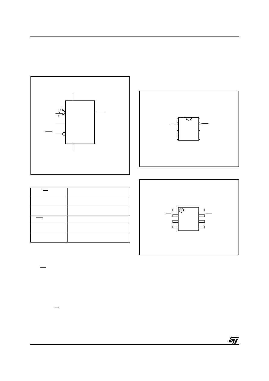
Figure 2. Logic Diagram
Table 1. Signal Names
These devices are compatible with a two-wire se-
rial interface that uses a bi-directional data bus
and serial clock. By setting the three chip enables
(E0, E1, E2) appropriately, up to eight 16 Kbit de-
vices can be attached to the same I
2
C bus, and
selected individually.
These devices behave as slave devices, with all
memory operations synchronized by the serial
clock. Read and Write operations are initiated by a
Start condition, generated by the bus master. The
Start condition is followed by a Device Select
Code and RW bit (as described in Table 2), termi-
nated by an acknowledge bit.
When writing data to the memory, the device in-
serts an acknowledge bit during the 9
th
bit time,
following the bus master's 8-bit transmission.
When data is read by the bus master, the bus
master acknowledges the receipt of the data byte
in the same way. Data transfers are terminated by
a Stop condition after an Ack for Write, and after a
NoAck for Read.
Figure 3. DIP Connections
Figure 4. SO Connections
Power On Reset: V
CC
Lock-Out Write Protect
In order to prevent data corruption and inadvertent
Write operations during Power-up, a Power On
Reset (POR) circuit is included. The internal reset
is held active until V
CC
has reached the POR
threshold value, and all operations are disabled ≠
the device will not respond to any command. In the
same way, when V
CC
drops from the operating
voltage, below the POR threshold value, all oper-
ations are disabled and the device will not respond
to any command. A stable and valid V
CC
must be
applied before applying any logic signal.
E0, E1, E2
Chip Enable
SDA
Serial Data
SCL
Serial Clock
WC
Write Control
V
CC
Supply Voltage
V
SS
Ground
AI02264
3
E0-E2
SDA
VCC
M24164
WC
SCL
VSS
SDA
VSS
SCL
WC
E1
E0
VCC
E2
AI02265B
M24164
1
2
3
4
8
7
6
5
1
AI02266B
2
3
4
8
7
6
5
SDA
VSS
SCL
WC
E1
E0
VCC
E2
M24164
3/21
M24164
SIGNAL DESCRIPTION
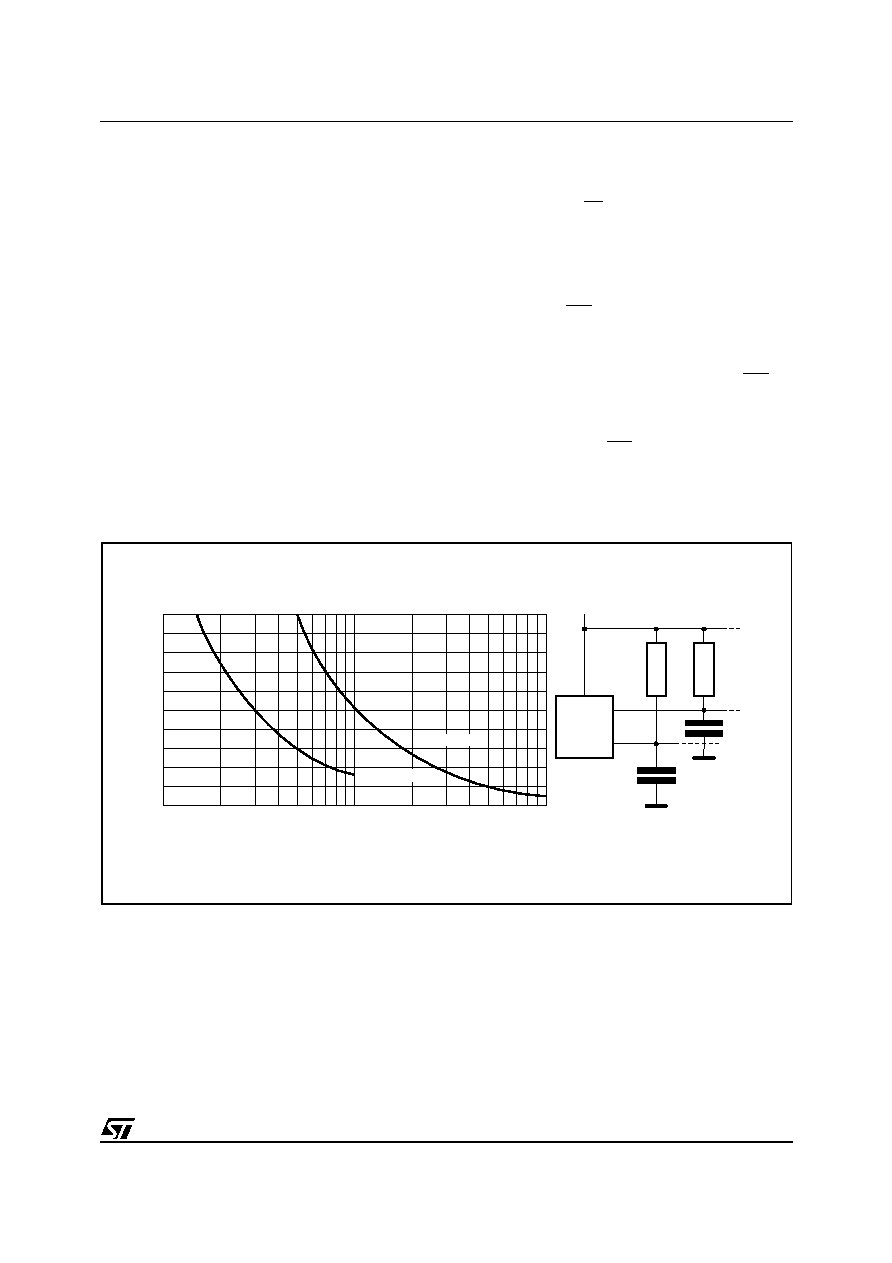
Serial Clock (SCL)
This input signal is used to strobe all data in and
out of the device. In applications where this signal
is used by slave devices to synchronize the bus to
a slower clock, the bus master must have an open
drain output, and a pull-up resistor must be con-
nected from Serial Clock (SCL) to V
CC
. (Figure 4
indicates how the value of the pull-up resistor can
be calculated). In most applications, though, this
method of synchronization is not employed, and
so the pull-up resistor is not necessary, provided
that the bus master has a push-pull (rather than
open drain) output.
Serial Data (SDA)
This bi-directional signal is used to transfer data in
or out of the device. It is an open drain output that
may be wire-OR'ed with other open drain or open
collector signals on the bus. A pull up resistor must
be connected from Serial Data (SDA) to V
CC
. (Fig-
ure 4 indicates how the value of the pull-up resistor
can be calculated).
Chip Enable (E0, E1, E2)
These input signals are used to set the value that
is to be looked for on three bits (b6, b5, b4) of the
7-bit Device Select Code. These inputs must be
tied to V
CC
or V
SS
, to establish the Device Select
Code.
Write Control (WC)
This input signal is useful for protecting the entire
contents of the memory from inadvertent write op-
erations. Write operations are disabled to the en-
tire memory array when Write Control (WC) is
driven High. When unconnected, the signal is in-
ternally read as V
IL
, and Write operations are al-
lowed.
When Write Control (WC) is driven High, Device
Select and Address bytes are acknowledged,
Data bytes are not acknowledged.
Figure 5. Maximum R
L
Value versus Bus Capacitance (C
BUS
) for an I
2
C Bus
AI01665
VCC
CBUS
SDA
RL
MASTER
RL
SCL
CBUS
100
0
4
8
12
16
20
CBUS (pF)
Maximum RP value (k
)
10
1000
fc = 400kHz
fc = 100kHz
M24164
4/21
DEVICE OPERATION
The device supports the I
2
C protocol. This is sum-
marized in Figure 2. Any device that sends data on
to the bus is defined to be a transmitter, and any
device that reads the data to be a receiver. The
device that controls the data transfer is known as
the bus master, and the other as the slave device.
A data transfer can only be initiated by the bus
master, which will also provide the serial clock for
synchronization. The M24164 device is always a
slave in all communication.
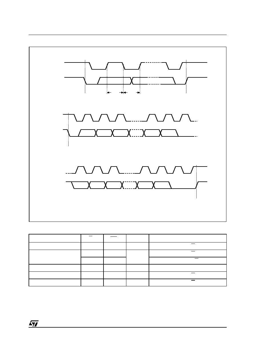
Start Condition
Start is identified by a falling edge of Serial Data
(SDA) while Serial Clock (SCL) is stable in the
High state. A Start condition must precede any
data transfer command. The device continuously
monitors (except during a Write cycle) Serial Data
(SDA) and Serial Clock (SCL) for a Start condition,
and will not respond unless one is given.
Stop Condition
Stop is identified by a rising edge of Serial Data
(SDA) while Serial Clock (SCL) is stable and driv-
en High. A Stop condition terminates communica-
tion between the device and the bus master. A
Read command that is followed by NoAck can be
followed by a Stop condition to force the device
into the Stand-by mode. A Stop condition at the
end of a Write command triggers the internal EE-
PROM Write cycle.
Acknowledge Bit (ACK)
The acknowledge bit is used to indicate a success-
ful byte transfer. The bus transmitter, whether it be
bus master or slave device, releases Serial Data
(SDA) after sending eight bits of data. During the
9
th
clock pulse period, the receiver pulls Serial
Data (SDA) Low to acknowledge the receipt of the
eight data bits.
Data Input
During data input, the device samples Serial Data
(SDA) on the rising edge of Serial Clock (SCL).
For correct device operation, Serial Data (SDA)
must be stable during the rising edge of Serial
Clock (SCL), and the Serial Data (SDA) signal
must change
only
when Serial Clock (SCL) is driv-
en Low.
Memory Addressing
To start communication between the bus master
and the slave device, the bus master must initiate
a Start condition. Following this, the bus master
sends eight bits, on Serial Data (SDA), most signif-
icant bit first. These consist of the 7-bit Device Se-
lect Code, and the Read/Write bit (RW), as shown
in Table 2. This last bit is set to 1 for Read, and 0
for Write operations.
The Device Select Code contains the three most
significant bits of the address within the memory
(A10, A9, A8), and a 3-bit Chip Enable "Address"
(E2, E1, E0).
When the Device Select Code is received on Seri-
al Data (SDA), the device only responds if the Chip
Enable Address is the same as the value on the
Chip Enable (E0, E2, and the inverse of E1) in-
puts. Up to eight devices can be connected on the
same bus, giving a total memory capacity of
128 Kbits, 16 KBytes.
If a match occurs on the Device Select code, the
corresponding device gives an acknowledgment
on Serial Data (SDA) during the 9
th
bit time. If the
device does not match the Device Select code, it
deselects itself from the bus, and goes into Stand-
by mode.
Table 2. Device Select Code
1
Note: 1. The most significant bit, b7, is sent first.
Device
Type
Identifier
Chip Enable Address
Most Significant Address Bits
RW
b7
b6
b5
b4
b3
b2
b1
b0
Device Select Code
1
E2
E1
E0
A10
A9
A8
RW
5/21
M24164
Figure 6. I
2
C Bus Protocol
Table 3. Operating Modes
Note: 1. X =
V
IH
or V
IL
.
Mode
RW bit
WC
1
Bytes
Initial Sequence
Current Address Read
1
X
1
START, Device Select, RW = 1
Random Address Read
0
X
1
START, Device Select, RW = 0, Address
1
X
reSTART, Device Select, RW = 1
Sequential Read
1
X
1
Similar to Current or Random Address Read
Byte Write
0
V
IL
1
START, Device Select, RW = 0
Page Write
0
V
IL
16
START, Device Select, RW = 0
SCL
SDA
SCL
SDA
SDA
START
Condition
SDA
Input
SDA
Change
AI00792B
STOP
Condition
1
2
3
7
8
9
MSB
ACK
START
Condition
SCL
1
2
3
7
8
9
MSB
ACK
STOP
Condition