 | –≠–ª–µ–∫—Ç—Ä–æ–Ω–Ω—ã–π –∫–æ–º–ø–æ–Ω–µ–Ω—Ç: M24256-A | –°–∫–∞—á–∞—Ç—å:  PDF PDF  ZIP ZIP |
1/20
PRELIMINARY DATA
April 2000
This is preliminary information on a new product now in development or undergoing evaluation. Details are subject to change without notice.
M24256-A
256 Kbit Serial I C Bus EEPROM
With Two Chip Enable Lines
s
Compatible with I
2
C Extended Addressing
s
Two Wire I
2
C Serial Interface
Supports 400 kHz Protocol
s
Single Supply Voltage:
≠ 4.5V to 5.5V for M24256-A
≠ 2.5V to 5.5V for M24256-AW
≠ 1.8V to 3.6V for M24256-AR
s
2 Chip Enable Inputs: up to four memories can
be connected to the same I
2
C bus
s
Hardware Write Control
s
BYTE and PAGE WRITE (up to 64 Bytes)
s
RANDOM and SEQUENTIAL READ Modes
s
Self-Timed Programming Cycle
s
Automatic Address Incrementing
s
Enhanced ESD/Latch-Up Behavior
s
More than 100,000 Erase/Write Cycles
s
More than 40 Year Data Retention
DESCRIPTION
These I
2
C-compatible electrically erasable pro-
grammable memory (EEPROM) devices are orga-
nized as 32Kx8 bits, and operate down to 2.5 V
(for the M24256-AW), and down to 1.8 V (for the
M24256-AR).
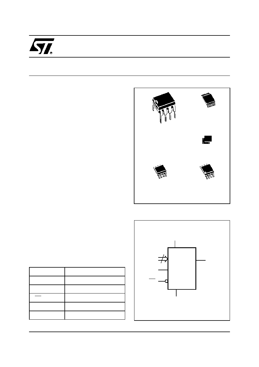
The M24256-A is available in Plastic Dual-in-Line,
Plastic Small Outline and Thin Shrink Small Out-
line packages. The M24256-A is also available in
a chip-scale (SBGA) package.
Figure 1. Logic Diagram
AI02271C
SDA
VCC
M24256-A
WC
SCL
VSS
2
E0-E1
Table 1. Signal Names
E0, E1
Chip Enable
SDA
Serial Data
SCL
Serial Clock
WC
Write Control
VCC
Supply Voltage
VSS
Ground
PSDIP8 (BN)
0.25 mm frame
SO8 (MN)
150 mil width
TSSOP14 (DL)
169 mil width
8
1
8
1
14
1
SO8 (MW)
200 mil width
8
1
SBGA
SBGA7 (EA)
140 x 90 mil
M24256-A
2/20
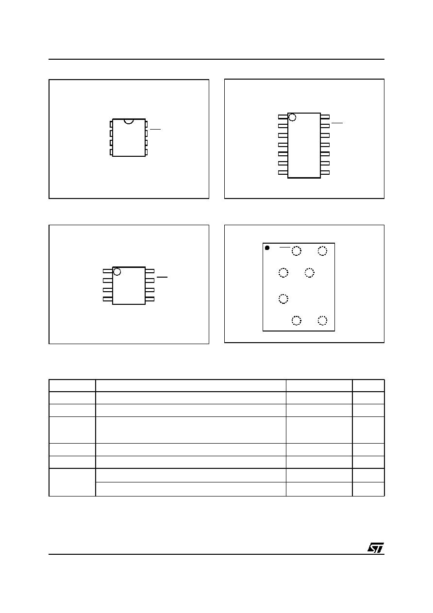
Figure 2A. DIP Connections
Note: 1. NC = Not Connected
Figure 2B. SO Connections
Note: 1. NC = Not Connected
SDA
VSS
SCL
WC
E1
E0
VCC
NC
AI02273C
M24256-A
1
2
3
4
8
7
6
5
1
AI02272C
2
3
4
8
7
6
5
SDA
VSS
SCL
WC
E1
E0
VCC
NC
M24256-A
Figure 2C. TSSOP Connections
Note: 1. NC = Not Connected
Figure 2D. SBGA Connections (top view)
1
AI02388C
2
3
4
14
9
10
8
SDA
VSS
NC
SCL
E0
WC
M24256-A
NC
E1
NC
NC
NC
NC
NC
5
6
7
12
13
11
VCC
AI03760
SCL
VSS
SDA
WC
VCC
M24256-A
S1
S0
Table 2. Absolute Maximum Ratings
1
Note: 1. Except for the rating "Operating Temperature Range", stresses above those listed in the Table "Absolute Maximum Ratings" may
cause permanent damage to the device. These are stress ratings only, and operation of the device at these or any other conditions
above those indicated in the Operating sections of this specification is not implied. Exposure to Absolute Maximum Rating condi-
tions for extended periods may affect device reliability. Refer also to the ST SURE Program and other relevant quality documents.
2. MIL-STD-883C, 3015.7 (100 pF, 1500
)
3. EIAJ IC-121 (Condition C) (200 pF, 0
)
Symbol
Parameter
Value
Unit
T
A
Ambient Operating Temperature
≠40 to 125
∞
C
T
STG
Storage Temperature
≠65 to 150
∞
C
T
LEAD
Lead Temperature during Soldering
PSDIP8: 10 sec
SO8: 40 sec
TSSOP14: t.b.c.
260
215
t.b.c.
∞
C
V
IO
Input or Output range
≠0.6 to 6.5
V
V
CC
Supply Voltage
≠0.3 to 6.5
V
V
ESD
Electrostatic Discharge Voltage (Human Body model)
2
4000
V
Electrostatic Discharge Voltage (Machine model)
3
200
V
3/20
M24256-A
These memory devices are compatible with the
I
2
C extended memory standard. This is a two wire
serial interface that uses a bi-directional data bus
and serial clock. The memory carries a built-in 4-
bit unique Device Type Identifier code (1010) in
accordance with the I
2
C bus definition.
The memory behaves as a slave device in the I
2
C
protocol, with all memory operations synchronized
by the serial clock. Read and Write operations are
initiated by a START condition, generated by the
bus master. The START condition is followed by a
Device Select Code and RW bit (as described in
Table 3), terminated by an acknowledge bit.
When writing data to the memory, the memory in-
serts an acknowledge bit during the 9
th
bit time,
following the bus master's 8-bit transmission.
When data is read by the bus master, the bus
master acknowledges the receipt of the data byte
in the same way. Data transfers are terminated by
a STOP condition after an Ack for WRITE, and af-
ter a NoAck for READ.
Power On Reset: V
CC
Lock-Out Write Protect
In order to prevent data corruption and inadvertent
write operations during power up, a Power On Re-
set (POR) circuit is included. The internal reset is
held active until the V
CC
voltage has reached the
POR threshold value, and all operations are dis-
abled ≠ the device will not respond to any com-
mand. In the same way, when V
CC
drops from the
operating voltage, below the POR threshold value,
all operations are disabled and the device will not
respond to any command. A stable and valid V
CC
must be applied before applying any logic signal.
SIGNAL DESCRIPTION
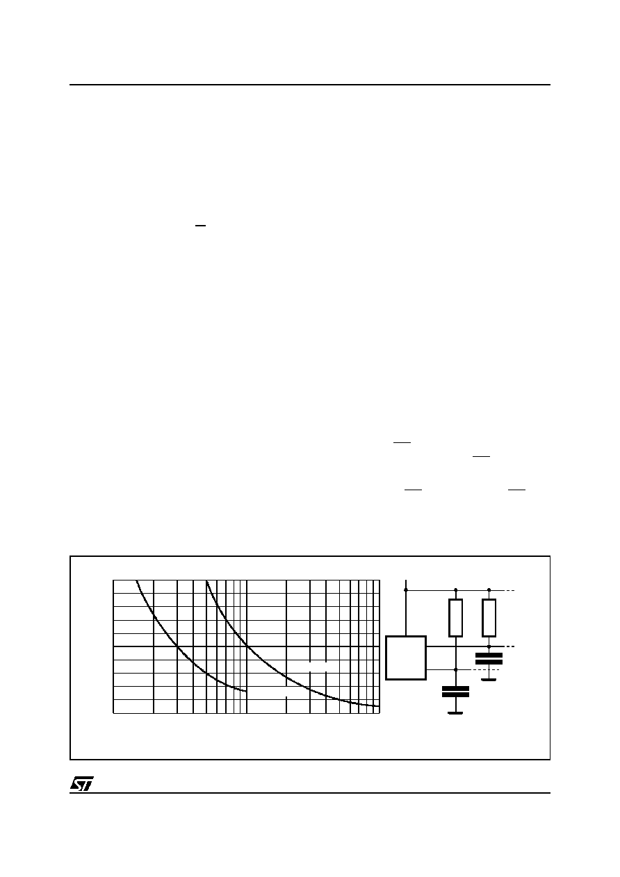
Serial Clock (SCL)
The SCL input pin is used to strobe all data in and
out of the memory. In applications where this line
is used by slaves to synchronize the bus to a slow-
er clock, the master must have an open drain out-
put, and a pull-up resistor must be connected from
the SCL line to V
CC
. (Figure 3 indicates how the
value of the pull-up resistor can be calculated). In
most applications, though, this method of synchro-
nization is not employed, and so the pull-up resis-
tor is not necessary, provided that the master has
a push-pull (rather than open drain) output.
Serial Data (SDA)
The SDA pin is bi-directional, and is used to trans-
fer data in or out of the memory. It is an open drain
output that may be wire-OR'ed with other open
drain or open collector signals on the bus. A pull
up resistor must be connected from the SDA bus
to V
CC
. (Figure 3 indicates how the value of the
pull-up resistor can be calculated).
Chip Enable (E1, E0)
These chip enable inputs are used to set the value
that is to be looked for on the two least significant
bits (b2, b1) of the 7-bit device select code. These
inputs must be tied to V
CC
or V
SS
to establish the
device select code. When unconnected, the E1
and E0 inputs are internally read as V
IL
(see Table
7 and Table 8)
Write Control (WC)
The hardware Write Control pin (WC) is useful for
protecting the entire contents of the memory from
inadvertent erase/write. The Write Control signal is
used to enable (WC=V
IL
) or disable (WC=V
IH
)
write instructions to the entire memory area. When
Figure 3. Maximum R
L
Value versus Bus Capacitance (C
BUS
) for an I
2
C Bus
AI01665
VCC
CBUS
SDA
RL
MASTER
RL
SCL
CBUS
100
0
4
8
12
16
20
CBUS (pF)
Maximum
RP
value
(k
)
10
1000
fc = 400kHz
fc = 100kHz
M24256-A
4/20
unconnected, the WC input is internally read as
V
IL
, and write operations are allowed.
When WC=1, Device Select and Address bytes
are acknowledged, Data bytes are not acknowl-
edged.
Please see the Application Note
AN404 for a more
detailed description of the Write Control feature.
DEVICE OPERATION
The memory device supports the I
2
C protocol.
This is summarized in Figure 4, and is compared
with other serial bus protocols in Application Note
AN1001. Any device that sends data on to the bus
is defined to be a transmitter, and any device that
reads the data to be a receiver. The device that
controls the data transfer is known as the master,
and the other as the slave. A data transfer can only
be initiated by the master, which will also provide
the serial clock for synchronization. The memory
device is always a slave device in all communica-
tion.
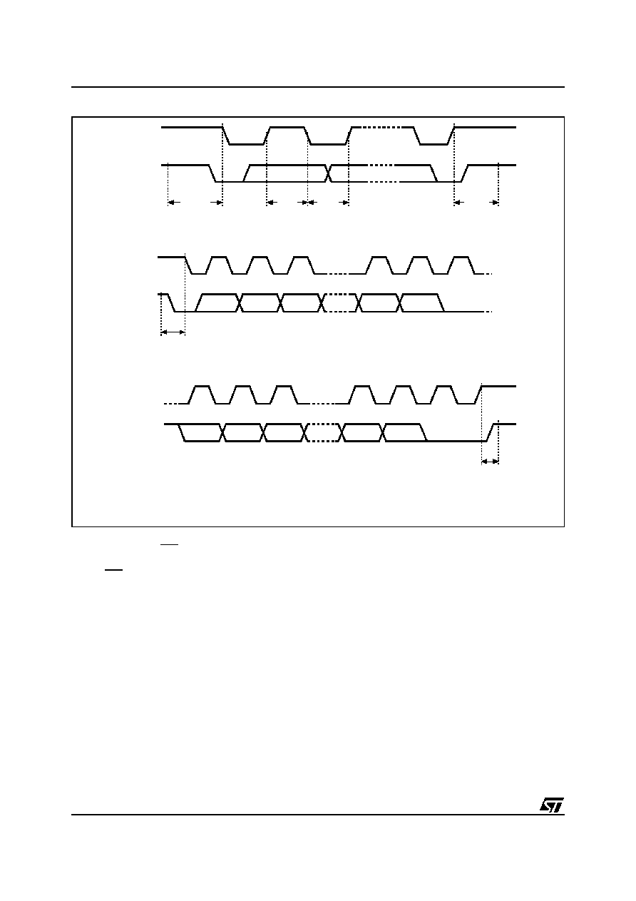
Start Condition
START is identified by a high to low transition of
the SDA line while the clock, SCL, is stable in the
high state. A START condition must precede any
data transfer command. The memory device con-
tinuously monitors (except during a programming
cycle) the SDA and SCL lines for a START condi-
tion, and will not respond unless one is given.
Stop Condition
STOP is identified by a low to high transition of the
SDA line while the clock SCL is stable in the high
state. A STOP condition terminates communica-
tion between the memory device and the bus mas-
ter. A STOP condition at the end of a Read
command, after (and only after) a NoAck, forces
the memory device into its standby state. A STOP
condition at the end of a Write command triggers
the internal EEPROM write cycle.
Figure 4. I
2
C Bus Protocol
SCL
SDA
SCL
SDA
SDA
START
CONDITION
SDA
INPUT
SDA
CHANGE
AI00792
STOP
CONDITION
1
2
3
7
8
9
MSB
ACK
START
CONDITION
SCL
1
2
3
7
8
9
MSB
ACK
STOP
CONDITION

5/20
M24256-A
Acknowledge Bit (ACK)
An acknowledge signal is used to indicate a suc-
cessful byte transfer. The bus transmitter, whether
it be master or slave, releases the SDA bus after
sending eight bits of data. During the 9
th
clock
pulse period, the receiver pulls the SDA bus low to
acknowledge the receipt of the eight data bits.
Data Input
During data input, the memory device samples the
SDA bus signal on the rising edge of the clock,
SCL. For correct device operation, the SDA signal
must be stable during the clock low-to-high transi-
tion, and the data must change
only when the SCL
line is low.
Memory Addressing
To start communication between the bus master
and the slave memory, the master must initiate a
START condition. Following this, the master sends
the 8-bit byte, shown in Table 3, on the SDA bus
line (most significant bit first). This consists of the
7-bit Device Select Code, and the 1-bit Read/Write
Designator (RW). The Device Select Code is fur-
ther subdivided into: a 4-bit Device Type Identifier,
and a 3-bit Chip Enable "Address" (0, E1, E0).
To address the memory array, the 4-bit Device
Type Identifier is 1010b.
Up to four memory devices can be connected on a
single I
2
C bus. Each one is given a unique 2-bit
code on its Chip Enable inputs. When the Device
Select Code is received on the SDA bus, the mem-
ory only responds if the Chip Select Code is the
same as the pattern applied to its Chip Enable
pins.
The 8
th
bit is the RW bit. This is set to `1' for read
and `0' for write operations. If a match occurs on
the Device Select Code, the corresponding mem-
ory gives an acknowledgment on the SDA bus dur-
ing the 9
th
bit time. If the memory does not match
the Device Select Code, it deselects itself from the
bus, and goes into stand-by mode.
There are two modes both for read and write.
These are summarized in Table 6 and described
later. A communication between the master and
the slave is ended with a STOP condition.
Each data byte in the memory has a 16-bit (two
byte wide) address. The Most Significant Byte (Ta-
ble 4) is sent first, followed by the Least significant
Byte (Table 5). Bits b15 to b0 form the address of
the byte in memory. Bit b15 is treated as Don't
Care bits on the M24256-A memory.
Write Operations
Following a START condition the master sends a
Device Select Code with the RW bit set to '0', as
shown in Table 6. The memory acknowledges this,
and waits for two address bytes. The memory re-
Table 3. Device Select Code
1
Note: 1. The most significant bit, b7, is sent first.
Device Type Identifier
Chip Enable
RW
b7
b6
b5
b4
b3
b2
b1
b0
Device Select Code
1
0
1
0
0
E1
E0
RW
Table 4. Most Significant Byte
Note: 1. b15 is treated as Don't Care on the M24256-A series.
Table 5. Least Significant Byte
b15
b14
b13
b12
b11
b10
b9
b8
b7
b6
b5
b4
b3
b2
b1
b0
Table 6. Operating Modes
Note: 1. X =
V
IH
or V
IL
.
Mode
RW bit
WC
1
Data Bytes
Initial Sequence
Current Address Read
1
X
1
START, Device Select, RW = 1
Random Address Read
0
X
1
START, Device Select, RW = 0, Address
1
X
reSTART, Device Select, RW = 1
Sequential Read
1
X
1
Similar to Current or Random Address Read
Byte Write
0
V
IL
1
START, Device Select, RW = 0
Page Write
0
V
IL
64
START, Device Select, RW = 0

M24256-A
6/20
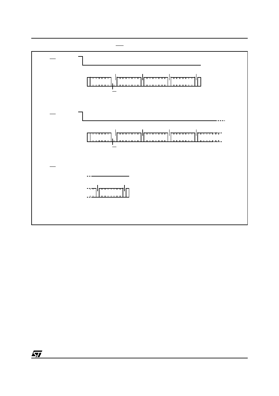
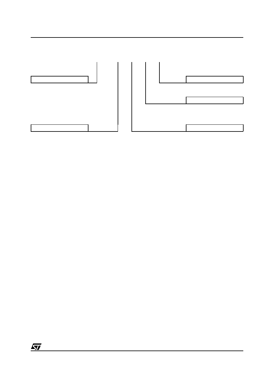
Figure 5. Write Mode Sequences with WC=1 (data write inhibited)
STOP
START
BYTE WRITE
DEV SEL
BYTE ADDR
BYTE ADDR
DATA IN
WC
START
PAGE WRITE
DEV SEL
BYTE ADDR
BYTE ADDR
DATA IN 1
WC
DATA IN 2
AI01120B
PAGE WRITE
(cont'd)
WC (cont'd)
STOP
DATA IN N
ACK
ACK
ACK
NO ACK
R/W
ACK
ACK
ACK
NO ACK
R/W
NO ACK
NO ACK
sponds to each address byte with an acknowledge
bit, and then waits for the data byte.
Writing to the memory may be inhibited if the WC
input pin is taken high. Any write command with
WC=1 (during a period of time from the START
condition until the end of the two address bytes)
will not modify the memory contents, and the ac-
companying data bytes will
not be acknowledged,
as shown in Figure 5.
Byte Write
In the Byte Write mode, after the Device Select
Code and the address bytes, the master sends
one data byte. If the addressed location is write
protected by the WC pin, the memory replies with
a NoAck, and the location is not modified. If, in-
stead, the WC pin has been held at 0, as shown in
Figure 6, the memory replies with an Ack. The
master terminates the transfer by generating a
STOP condition.
Page Write
The Page Write mode allows up to 64 bytes to be
written in a single write cycle, provided that they
are all located in the same 'row' in the memory:
that is the most significant memory address bits
(b14-b6 for the M24256-A) are the same. If more
bytes are sent than will fit up to the end of the row,
a condition known as `roll-over' occurs. Data starts
to become overwritten (in a way not formally spec-
ified in this data sheet).
The master sends from one up to 64 bytes of data,
each of which is acknowledged by the memory if
the WC pin is low. If the WC pin is high, the con-
tents of the addressed memory location are not
modified, and each data byte is followed by a
NoAck. After each byte is transferred, the internal
byte address counter (the 6 least significant bits
only) is incremented. The transfer is terminated by
the master generating a STOP condition.
When the master generates a STOP condition im-
mediately after the Ack bit (in the "10
th
bit" time
7/20
M24256-A
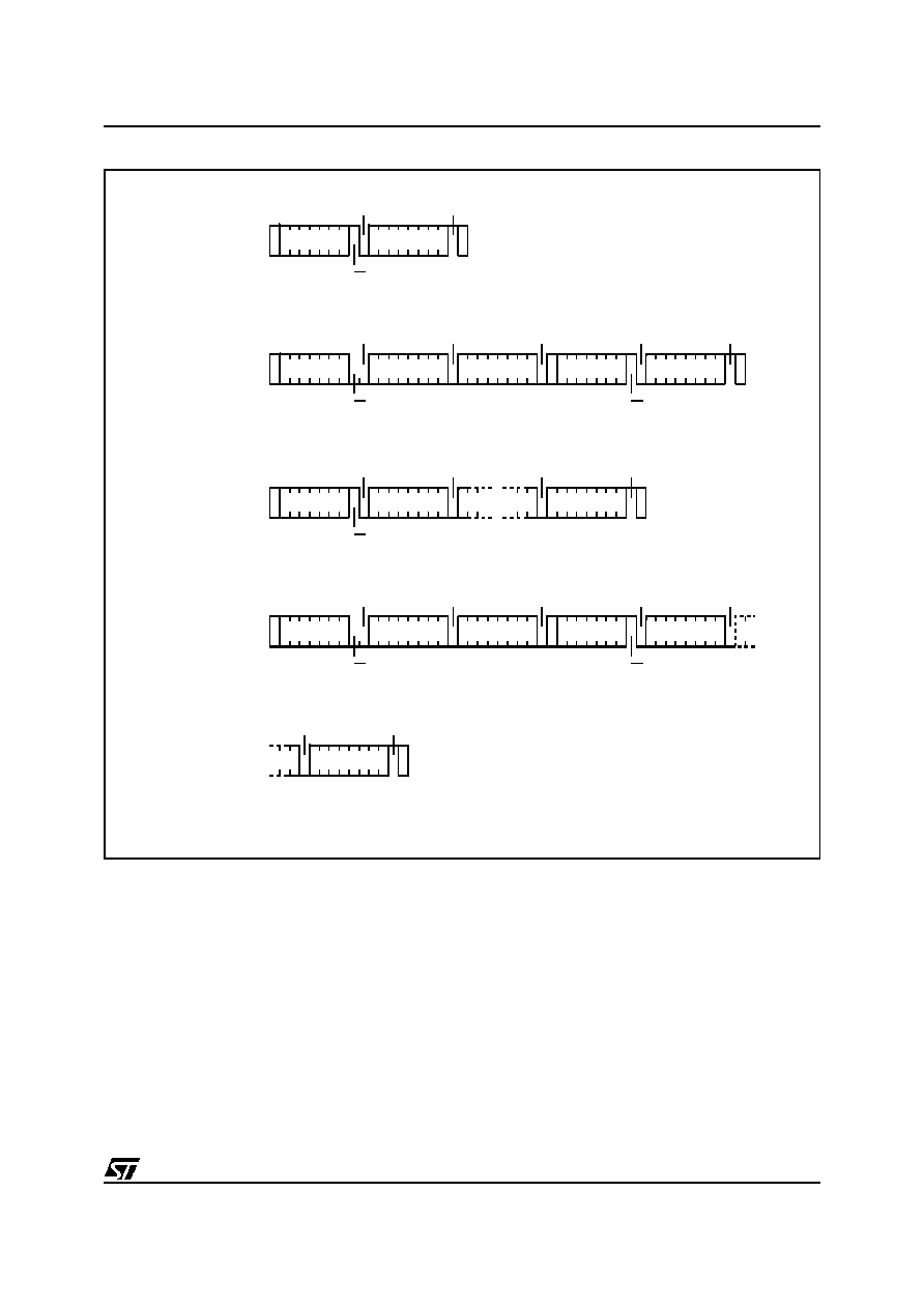
Figure 6. Write Mode Sequences with WC=0 (data write enabled)
STOP
START
BYTE WRITE
DEV SEL
BYTE ADDR
BYTE ADDR
DATA IN
WC
START
PAGE WRITE
DEV SEL
BYTE ADDR
BYTE ADDR
DATA IN 1
WC
DATA IN 2
AI01106B
PAGE WRITE
(cont'd)
WC (cont'd)
STOP
DATA IN N
ACK
R/W
ACK
ACK
ACK
ACK
ACK
ACK
ACK
R/W
ACK
ACK
slot), either at the end of a byte write or a page
write, the internal memory write cycle is triggered.
A STOP condition at any other time does not trig-
ger the internal write cycle.
During the internal write cycle, the SDA input is
disabled internally, and the device does not re-
spond to any requests.
M24256-A
8/20
Read Operations
Read operations are performed independently of
the state of the WC pin.
Random Address Read
A dummy write is performed to load the address
into the address counter, as shown in Figure 8.
Then,
without sending a STOP condition, the mas-
ter sends another START condition, and repeats
the Device Select Code, with the RW bit set to `1'.
The memory acknowledges this, and outputs the
contents of the addressed byte. The master must
not acknowledge the byte output, and terminates
the transfer with a STOP condition.
Current Address Read
The device has an internal address counter which
is incremented each time a byte is read. For the
Current Address Read mode, following a START
condition, the master sends a Device Select Code
with the RW bit set to `1'. The memory acknowl-
edges this, and outputs the byte addressed by the
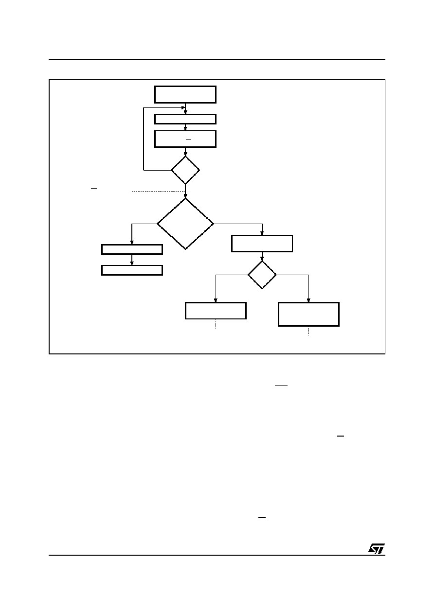
Minimizing System Delays by Polling On ACK
During the internal write cycle, the memory discon-
nects itself from the bus, and copies the data from
its internal latches to the memory cells. The maxi-
mum write time (t
w
) is shown in Table 9, but the
typical time is shorter. To make use of this, an Ack
polling sequence can be used by the master.
The sequence, as shown in Figure 7, is:
≠ Initial condition: a Write is in progress.
≠ Step 1: the master issues a START condition
followed by a Device Select Code (the first byte
of the new instruction).
≠ Step 2: if the memory is busy with the internal
write cycle, no Ack will be returned and the mas-
ter goes back to Step 1. If the memory has ter-
minated the internal write cycle, it responds with
an Ack, indicating that the memory is ready to
receive the second part of the next instruction
(the first byte of this instruction having been sent
during Step 1).
Figure 7. Write Cycle Polling Flowchart using ACK
WRITE Cycle
in Progress
AI01847
Next
Operation is
Addressing the
Memory
START Condition
DEVICE SELECT
with RW = 0
ACK
Returned
YES
NO
YES
NO
ReSTART
STOP
Proceed
WRITE Operation
Proceed
Random Address
READ Operation
Send
Byte Address
First byte of instruction
with RW = 0 already
decoded by M24xxx
9/20
M24256-A
The output data comes from consecutive address-
es, with the internal address counter automatically
incremented after each byte output. After the last
memory address, the address counter `rolls-over'
and the memory continues to output data from
memory address 00h.
Acknowledge in Read Mode
In all read modes, the memory waits, after each
byte read, for an acknowledgment during the 9
th
bit time. If the master does not pull the SDA line
low during this time, the memory terminates the
data transfer and switches to its stand-by state.
internal address counter. The counter is then in-
cremented. The master terminates the transfer
with a STOP condition, as shown in Figure 8,
with-
out acknowledging the byte output.
Sequential Read
This mode can be initiated with either a Current
Address Read or a Random Address Read. The
master
does acknowledge the data byte output in
this case, and the memory continues to output the
next byte in sequence. To terminate the stream of
bytes, the master must
not acknowledge the last
byte output, and
must generate a STOP condition.
Figure 8. Read Mode Sequences
Note: 1. The seven most significant bits of the Device Select Code of a Random Read (in the 1
st
and 4
th
bytes) must be identical.
START
DEV SEL *
BYTE ADDR
BYTE ADDR
START
DEV SEL
DATA OUT 1
AI01105C
DATA OUT N
STOP
START
CURRENT
ADDRESS
READ
DEV SEL
DATA OUT
RANDOM
ADDRESS
READ
STOP
START
DEV SEL *
DATA OUT
SEQUENTIAL
CURRENT
READ
STOP
DATA OUT N
START
DEV SEL *
BYTE ADDR
BYTE ADDR
SEQUENTIAL
RANDOM
READ
START
DEV SEL *
DATA OUT 1
STOP
ACK
R/W
NO ACK
ACK
R/W
ACK
ACK
ACK
R/W
ACK
ACK
ACK
NO ACK
R/W
NO ACK
ACK
ACK
ACK
R/W
ACK
ACK
R/W
ACK
NO ACK
M24256-A
10/20
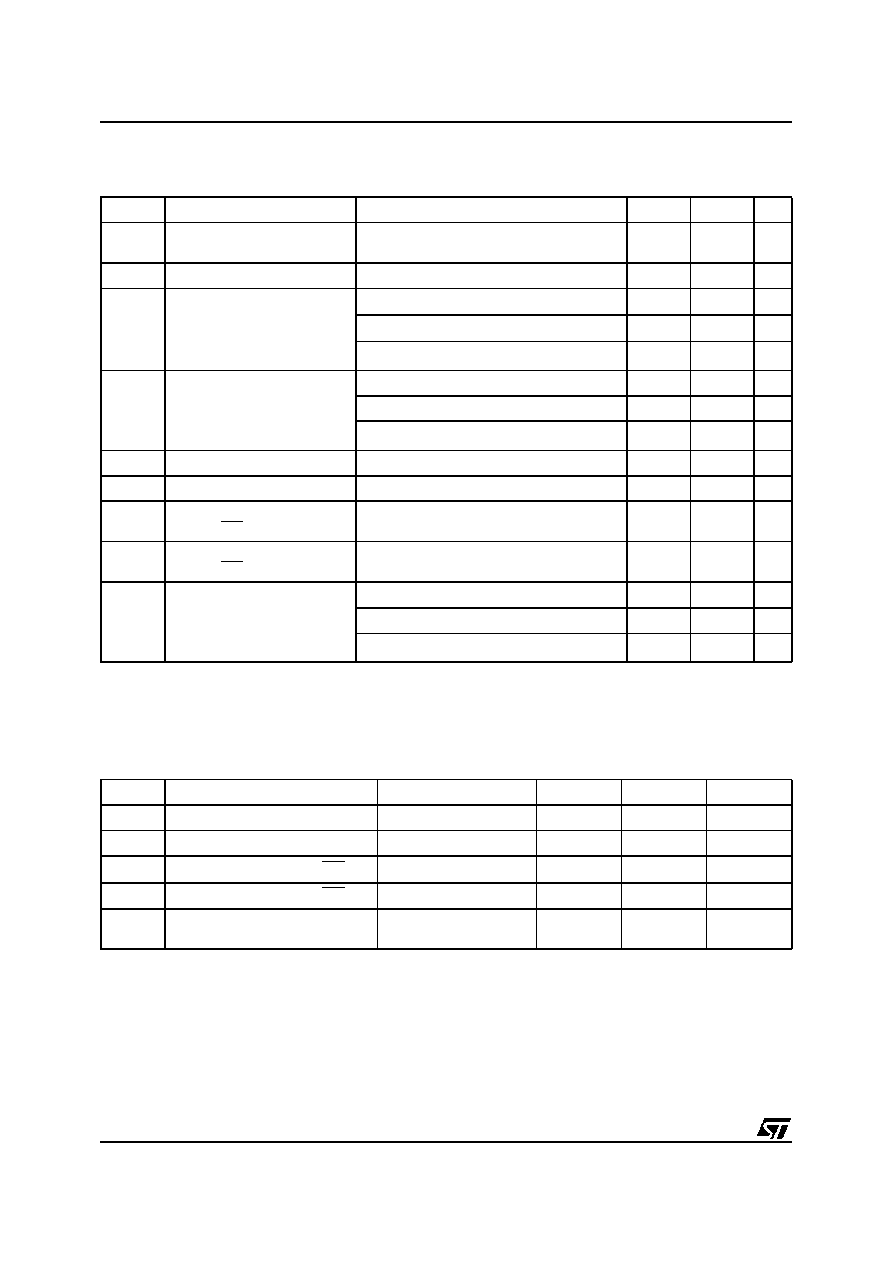
Table 7. DC Characteristics
(T
A
= ≠40 to 85
∞
C; V
CC
= 4.5 to 5.5 V or 2.5 to 5.5 V)
(T
A
= ≠20 to 85
∞
C; V
CC
= 1.8 to 3.6 V)
Note: 1. This is preliminary data.
Table 8. Input Parameters
1
(T
A
= 25
∞
C, f = 400 kHz)
Note: 1. Sampled only, not 100% tested.
Symbol
Parameter
Test Condition
Min.
Max.
Unit
I
LI
Input Leakage Current
(SCL, SDA)
0 V
V
IN
V
CC
±
2
µ
A
I
LO
Output Leakage Current
0 V
V
OUT
V
CC,
SDA in Hi-Z
±
2
µ
A
I
CC
Supply Current
V
CC
=5V, f
c
=400kHz (rise/fall time < 30ns)
2
mA
-W series:
V
CC
=2.5V, f
c
=400kHz (rise/fall time < 30ns)
1
mA
-R series:
V
CC
=1.8V, f
c
=100kHz (rise/fall time < 30ns)
0.5
1
mA
I
CC1
Supply Current
(Stand-by)
V
IN
= V
SS
or V
CC
, V
CC
= 5 V
10
µ
A
-W series:
V
IN
= V
SS
or V
CC
, V
CC
= 2.5 V
2
µ
A
-R series:
V
IN
= V
SS
or V
CC
, V
CC
= 1.8 V
1
1
µ
A
V
IL
Input Low Voltage (SCL, SDA)
≠0.3
0.3V
CC
V
V
IH
Input High Voltage (SCL, SDA)
0.7V
CC
V
CC
+1
V
V
IL
Input Low Voltage
(E0, E1, WC)
≠0.3
0.5
V
V
IH
Input High Voltage
(E0, E1, WC)
0.7V
CC
V
CC
+1
V
V
OL
Output Low
Voltage
I
OL
= 3 mA, V
CC
= 5 V
0.4
V
-W series:
I
OL
= 2.1 mA, V
CC
= 2.5 V
0.4
V
-R series:
I
OL
= 0.7 mA, V
CC
= 1.8 V
0.2
1
V
Symbol
Parameter
Test Condition
Min.
Max.
Unit
C
IN
Input Capacitance (SDA)
8
pF
C
IN
Input Capacitance (other pins)
6
pF
Z
L
Input Impedance (E1, E0, WC)
V
IN
0.5 V
50
k
Z
H
Input Impedance (E1, E0, WC)
V
IN
0.7V
CC
500
k
t
NS
Pulse width ignored
(Input Filter on SCL and SDA)
Single glitch
100
ns
11/20
M24256-A
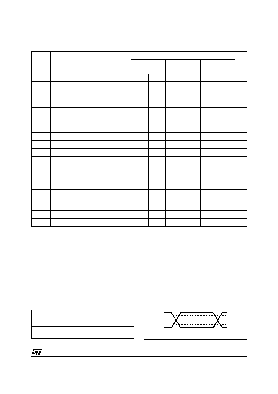
Table 9. AC Characteristics
Note: 1. For a reSTART condition, or following a write cycle.
2. Sampled only, not 100% tested.
3. To avoid spurious STAR T and STOP conditions, a minimum delay is placed between SCL=1 and the falling or rising edge of SDA.
4. This is preliminary data.
Symbol
Alt.
Parameter
M24256-A
Unit
V
CC
=4.5 to 5.5 V
T
A
=≠40 to 85
∞
C
V
CC
=2.5 to 5.5 V
T
A
=≠40 to 85
∞
C
V
CC
=1.8 to 3.6 V
T
A
=≠20 to 85
∞
C
4
Min
Max
Min
Max
Min
Max
t
CH1CH2
t
R
Clock Rise Time
300
300
1000
ns
t
CL1CL2
t
F
Clock Fall Time
300
300
300
ns
t
DH1DH2
2
t
R
SDA Rise Time
20
300
20
300
20
1000
ns
t
DL1DL2
2
t
F
SDA Fall Time
20
300
20
300
20
300
ns
t
CHDX
1
t
SU:STA
Clock High to Input Transition
600
600
4700
ns
t
CHCL
t
HIGH
Clock Pulse Width High
600
600
4000
ns
t
DLCL
t
HD:STA
Input Low to Clock Low (START)
600
600
4000
ns
t
CLDX
t
HD:DAT
Clock Low to Input Transition
0
0
0
µ
s
t
CLCH
t
LOW
Clock Pulse Width Low
1.3
1.3
4.7
µ
s
t
DXCX
t
SU:DAT
Input Transition to Clock
Transition
100
100
250
ns
t
CHDH
t
SU:STO
Clock High to Input High (STOP)
600
600
4000
ns
t
DHDL
t
BUF
Input High to Input Low (Bus
Free)
1.3
1.3
4.7
µ
s
t
CLQV
3
t
AA
Clock Low to Data Out Valid
200
900
200
900
200
3500
ns
t
CLQX
t
DH
Data Out Hold Time After Clock
Low
200
200
200
ns
f
C
f
SCL
Clock Frequency
400
400
100
kHz
t
W
t
WR
Write Time
10
10
10
ms
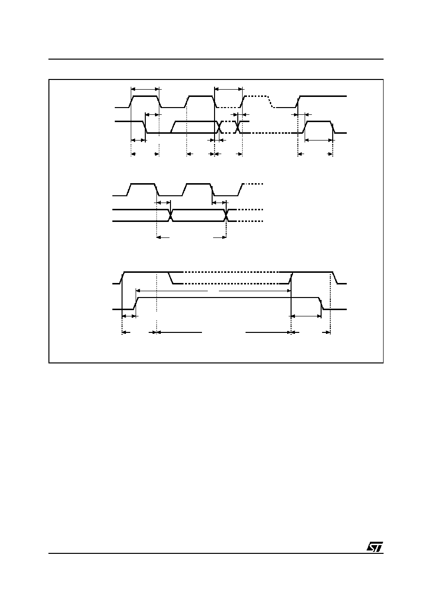
Table 10. AC Measurement Conditions
Input Rise and Fall Times
50 ns
Input Pulse Voltages
0.2V
CC
to 0.8V
CC
Input and Output Timing
Reference Voltages
0.3V
CC
to 0.7V
CC
Figure 9. AC Testing Input Output Waveforms
AI00825
0.8VCC
0.2VCC
0.7VCC
0.3VCC
M24256-A
12/20
Figure 10. AC Waveforms
SCL
SDA IN
SCL
SDA OUT
SCL
SDA IN
tCHCL
tDLCL
tCHDX
START
CONDITION
tCLCH
tDXCX
tCLDX
SDA
INPUT
SDA
CHANGE
tCHDH
tDHDL
STOP &
BUS FREE
DATA VALID
tCLQV
tCLQX
DATA OUTPUT
tCHDH
STOP
CONDITION
tCHDX
START
CONDITION
WRITE CYCLE
tW
AI00795B
13/20
M24256-A
Table 11. Ordering Information Scheme
Note: 1. SBGA7 package available only for the "M24256-A W EA 6 T"
Example:
M24256
≠ A
W
MN
6
T
Memory Capacity
Option
256
256 Kbit (32K x 8)
T
Tape and Reel Packing
Temperature Range
6
≠40
∞
C to 85
∞
C
5
≠20
∞
C to 85
∞
C
Operating Voltage
Package
blank 4.5 V to 5.5 V
BN
PSDIP8 (0.25 mm frame)
W
2.5 V to 5.5 V
MN
SO8 (150 mil width)
R
1.8 V to 3.6 V
MW
SO8 (200 mil width)
DL
TSSOP14 (169 mil width)
EA
SBGA7
1
ORDERING INFORMATION
Devices are shipped from the factory with the
memory content set at all 1s (FFh).
The notation used for the device number is as
shown in Table 11. For a list of available options
(speed, package, etc.) or for further information on
any aspect of this device, please contact your
nearest ST Sales Office.
M24256-A
14/20
Figure 11. PSDIP8 (BN)
Note:
1. Drawing is not to scale.
PSDIP-a
A2
A1
A
L
e1
D
E1
E
N
1
C
eA
eB
B1
B
Table 12. PSDIP8 - 8 pin Plastic Skinny DIP, 0.25mm lead frame
Symb.
mm
inches
Typ.
Min.
Max.
Typ.
Min.
Max.
A
3.90
5.90
0.154
0.232
A1
0.49
≠
0.019
≠
A2
3.30
5.30
0.130
0.209
B
0.36
0.56
0.014
0.022
B1
1.15
1.65
0.045
0.065
C
0.20
0.36
0.008
0.014
D
9.20
9.90
0.362
0.390
E
7.62
≠
≠
0.300
≠
≠
E1
6.00
6.70
0.236
0.264
e1
2.54
≠
≠
0.100
≠
≠
eA
7.80
≠
0.307
≠
eB
10.00
0.394
L
3.00
3.80
0.118
0.150
N
8
8
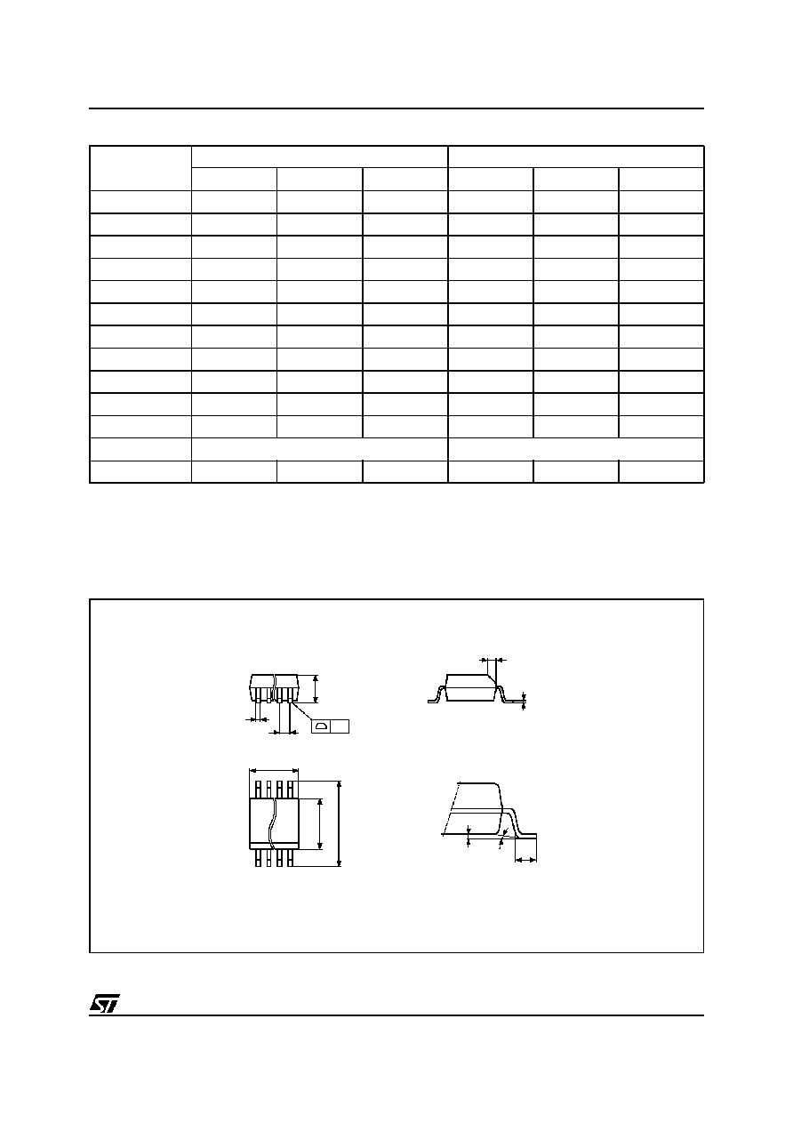
15/20
M24256-A
Table 13. SO8 - 8 lead Plastic Small Outline, 150 mils body width
Symb.
mm
inches
Typ.
Min.
Max.
Typ.
Min.
Max.
A
1.35
1.75
0.053
0.069
A1
0.10
0.25
0.004
0.010
B
0.33
0.51
0.013
0.020
C
0.19
0.25
0.007
0.010
D
4.80
5.00
0.189
0.197
E
3.80
4.00
0.150
0.157
e
1.27
≠
≠
0.050
≠
≠
H
5.80
6.20
0.228
0.244
h
0.25
0.50
0.010
0.020
L
0.40
0.90
0.016
0.035
0
∞
8
∞
0
∞
8
∞
N
8
8
CP
0.10
0.004
Figure 12. SO8 narrow (MN)
Note:
1. Drawing is not to scale.
SO-a
E
N
CP
B
e
A
D
C
L
A1
1
H
h x 45
∞
M24256-A
16/20
Table 14. SO8 - 8 lead Plastic Small Outline, 200 mils body width
Symb.
mm
inches
Typ.
Min.
Max.
Typ.
Min.
Max.
A
2.03
0.080
A1
0.10
0.25
0.004
0.010
A2
1.78
0.070
B
0.35
0.45
0.014
0.018
C
0.20
≠
≠
0.008
≠
≠
D
5.15
5.35
0.203
0.211
E
5.20
5.40
0.205
0.213
e
1.27
≠
≠
0.050
≠
≠
H
7.70
8.10
0.303
0.319
L
0.50
0.80
0.020
0.031
0
∞
10
∞
0
∞
10
∞
N
8
8
CP
0.10
0.004
Figure 13. SO8 wide (MW)
Note:
1. Drawing is not to scale.
SO-b
E
N
CP
B
e
A2
D
C
L
A1
H
A
1
17/20
M24256-A
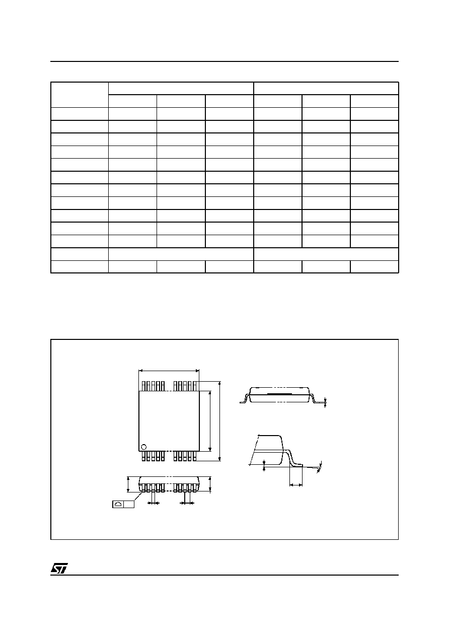
Table 15. TSSOP14 - 14 lead Thin Shrink Small Outline
Symb.
mm
inches
Typ.
Min.
Max.
Typ.
Min.
Max.
A
1.10
0.043
A1
0.05
0.15
0.002
0.006
A2
0.85
0.95
0.033
0.037
B
0.19
0.30
0.007
0.012
C
0.09
0.20
0.004
0.008
D
4.90
5.10
0.193
0.197
E
6.25
6.50
0.246
0.256
E1
4.30
4.50
0.169
0.177
e
0.65
≠
≠
0.026
≠
≠
L
0.50
0.70
0.020
0.028
0
∞
8
∞
0
∞
8
∞
N
14
14
CP
0.08
0.003
Figure 14. TSSOP14 (DL)
Note:
1. Drawing is not to scale.
TSSOP
1
N
CP
N/2
DIE
C
L
A1
E
E1
D
A2
A
e
B
M24256-A
18/20
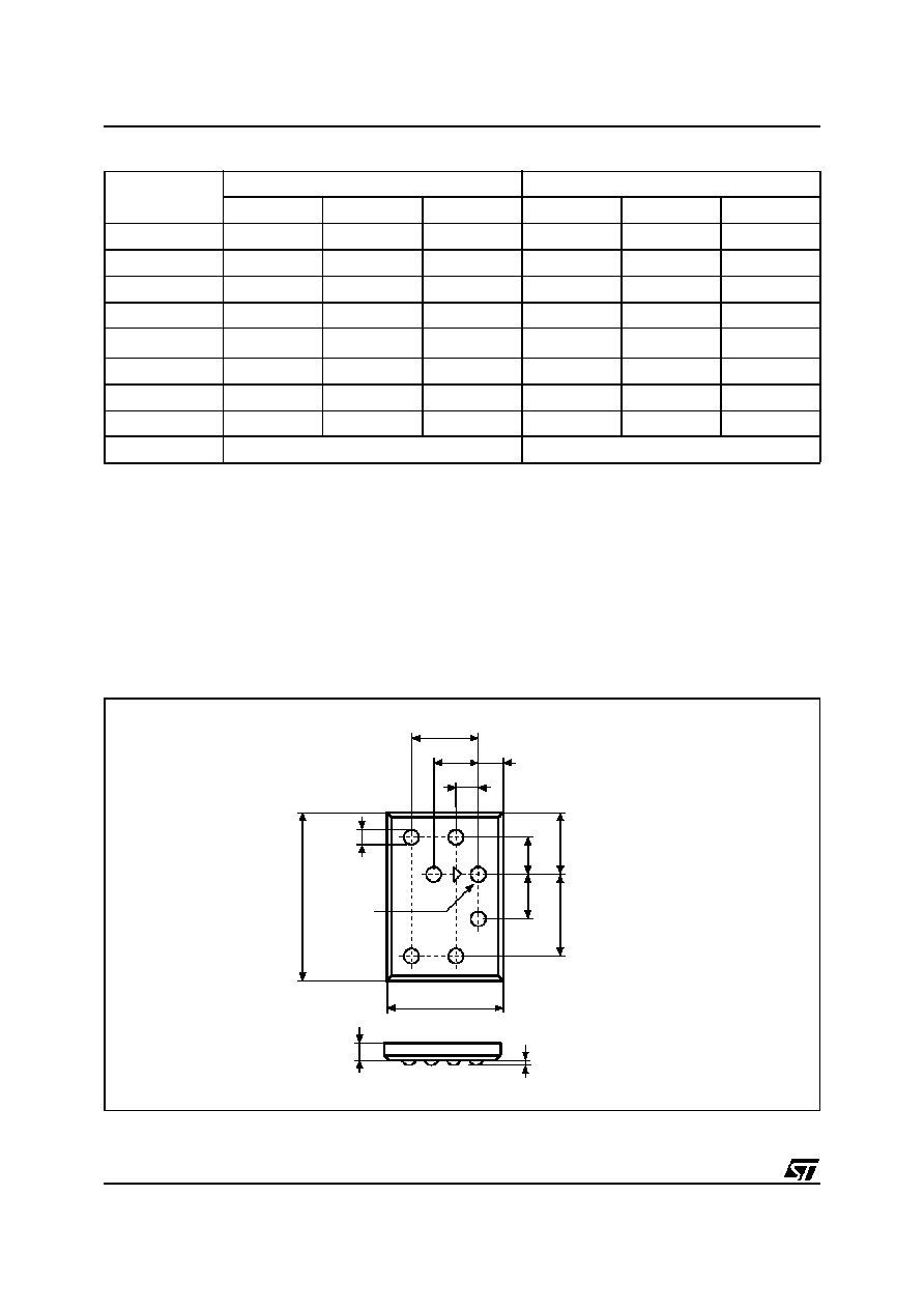
Table 16. SBGA7 - 7 ball Shell Ball Grid Array
Note: 1. No ball is closer than D2 to any other ball, thus giving an arrangement of equilateral triangles in which:
E1 = D2/2 ; E2 = D2 ; E3 = 3xD2/2
D3 =
3xD2/2 ; D1 = D2 +
3xD2/2
Symb.
mm
inches
Typ.
Min.
Max.
Typ.
Min.
Max.
A
0.430
0.380
0.480
0.017
0.015
0.019
A1
0.180
0.150
0.210
0.007
0.006
0.008
b
0.350
0.320
0.380
0.014
0.013
0.015
D
3.555
3.525
3.585
0.140
0.138
0.142
D2
1
1.000
0.970
1.030
0.039
0.038
0.041
E
2.275
2.245
2.305
0.090
0.088
0.091
FD
1.278
--
--
0.050
--
--
FE
0.388
--
--
0.015
--
--
N
7
7
Figure 15. SBGA7 (EA) ≠ Underside view (ball side)
Note: 1. Drawing is not to scale.
A
SBGA-01
A1
BALL "1"
b
D2
D3
E1
E
E3
E2
D
D1
FD
FE

19/20
M24256-A
Table 17. Revision History
Date
Description of Revision
17-Apr-2000
SBGA7(EA) package added on pp 1, 2, OrderInfo, PackageData
E1 and E0 are specified as having to be tied either to V
CC
or V
SS

M24256-A
20/20
Information furnished is believed to be accurate and reliable. However, STMi croelectronics assumes no responsibility for the consequences
of use of such information nor for any infringement of patents or other rights of third parties which may result from its use. No license is granted
by implication or otherwise under any patent or patent rights of STMicroelectronics. Specifications mentioned in this publication are subject
to change without notice. This publication supersedes and replaces all information previously supplied. STMicroelectronics products are not
authorized for use as criti cal components in life support devices or systems without express writt en approval of STMicroelectronics.
©
2000 STMicroelectronics - All Rights Reserved
The ST logo is a registered trademark of STMicroelectronics.
All other names are the property of their respective owners.
STMicroelectronics GROUP OF COMPANIES
Australia - Brazil - China - Finland - France - Germany - Hong Kong - India - Italy - Japan - Malaysia - Malta - Morocco - Singapore - Spain -
Sweden - Switzerland - United Kingdom - U.S.A.
http:// www.st.com