 | –≠–ª–µ–∫—Ç—Ä–æ–Ω–Ω—ã–π –∫–æ–º–ø–æ–Ω–µ–Ω—Ç: M24512-R | –°–∫–∞—á–∞—Ç—å:  PDF PDF  ZIP ZIP |
Document Outline
- FEATURES SUMMARY
- TABLE OF CONTENTS
- SUMMARY DESCRIPTION
- SIGNAL DESCRIPTION
- DEVICE OPERATION
- INITIAL DELIVERY STATE
- MAXIMUM RATING
- DC and AC PARAMETERS
- PACKAGE MECHANICAL
- Figure 12. PDIP8 Ö 8 pin Plastic DIP, 0.25mm lead frame, Package Outline
- Table 16. PDIP8 Ö 8 pin Plastic DIP, 0.25mm lead frame, Package Mechanical Data
- Figure 13. SO8 wide Ö 8 lead Plastic Small Outline, 200 mils body width, Package Outline
- Table 17. SO8 wide Ö 8 lead Plastic Small Outline, 200 mils body width, Package Mechanical Data
- Figure 14. LGA8 - 8 lead Land Grid Array, Package Outline
- Table 18. LGA8 - 8 lead Land Grid Array, Package Mechanical Data
- PART NUMBERING
- REVISION HISTORY
1/24
October 2003
M24512
512 Kbit Serial I≤C Bus EEPROM
FEATURES SUMMARY
s
Two Wire I
2
C Serial Interface
Supports 400 kHz Protocol
s
Single Supply Voltage:
≠ 4.5V to 5.5V for M24512
≠ 2.5V to 5.5V for M24512-W
≠ 1.8V to 3.6V for M24512-S
s
Write Control Input
s
BYTE and PAGE WRITE (up to 128 Bytes)
s
RANDOM and SEQUENTIAL READ Modes
s
Self-Timed Programming Cycle
s
Automatic Address Incrementing
s
Enhanced ESD/Latch-Up Behavior
s
More than 100,000 Erase/Write Cycles
s
More than 40 Year Data Retention
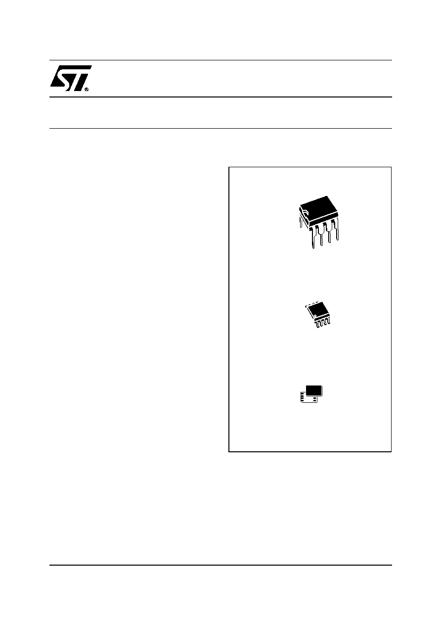
Figure 1. Packages
PDIP8 (BN)
8
1
SO8 (MW)
200 mil width
LGA8 (LA)
8
1
LGA

M24512
2/24
TABLE OF CONTENTS
FEATURES SUMMARY . . . . . . . . . . . . . . . . . . . . . . . . . . . . . . . . . . . . . . . . . . . . . . . . . . . . . . . . . . . . . 1
Figure 1. Packages . . . . . . . . . . . . . . . . . . . . . . . . . . . . . . . . . . . . . . . . . . . . . . . . . . . . . . . . . . . . . . 1
SUMMARY DESCRIPTION . . . . . . . . . . . . . . . . . . . . . . . . . . . . . . . . . . . . . . . . . . . . . . . . . . . . . . . . . . . 4
Figure 2. Logic Diagram . . . . . . . . . . . . . . . . . . . . . . . . . . . . . . . . . . . . . . . . . . . . . . . . . . . . . . . . . . 4
Table 1. Signal Names . . . . . . . . . . . . . . . . . . . . . . . . . . . . . . . . . . . . . . . . . . . . . . . . . . . . . . . . . . . 4
Power On Reset: VCC Lock-Out Write Protect . . . . . . . . . . . . . . . . . . . . . . . . . . . . . . . . . . . . . . . 4
Figure 3. DIP, SO and LGA Connections . . . . . . . . . . . . . . . . . . . . . . . . . . . . . . . . . . . . . . . . . . . . . 4
SIGNAL DESCRIPTION . . . . . . . . . . . . . . . . . . . . . . . . . . . . . . . . . . . . . . . . . . . . . . . . . . . . . . . . . . . . . 5
Serial Clock (SCL) . . . . . . . . . . . . . . . . . . . . . . . . . . . . . . . . . . . . . . . . . . . . . . . . . . . . . . . . . . . . . . . 5
Serial Data (SDA) . . . . . . . . . . . . . . . . . . . . . . . . . . . . . . . . . . . . . . . . . . . . . . . . . . . . . . . . . . . . . . . 5
Chip Enable (E0, E1, E2) . . . . . . . . . . . . . . . . . . . . . . . . . . . . . . . . . . . . . . . . . . . . . . . . . . . . . . . . . 5
Write Control (WC) . . . . . . . . . . . . . . . . . . . . . . . . . . . . . . . . . . . . . . . . . . . . . . . . . . . . . . . . . . . . . . 5
Figure 4. Maximum RL Value versus Bus Capacitance (CBUS) for an I2C Bus . . . . . . . . . . . . . . . . 5
Figure 5. I2C Bus Protocol . . . . . . . . . . . . . . . . . . . . . . . . . . . . . . . . . . . . . . . . . . . . . . . . . . . . . . . . 6
Table 2. Device Select Code . . . . . . . . . . . . . . . . . . . . . . . . . . . . . . . . . . . . . . . . . . . . . . . . . . . . . . . 6
Table 3. Most Significant Byte . . . . . . . . . . . . . . . . . . . . . . . . . . . . . . . . . . . . . . . . . . . . . . . . . . . . . . 6
Table 4. Least Significant Byte . . . . . . . . . . . . . . . . . . . . . . . . . . . . . . . . . . . . . . . . . . . . . . . . . . . . . 6
DEVICE OPERATION . . . . . . . . . . . . . . . . . . . . . . . . . . . . . . . . . . . . . . . . . . . . . . . . . . . . . . . . . . . . . . . 7
Start Condition. . . . . . . . . . . . . . . . . . . . . . . . . . . . . . . . . . . . . . . . . . . . . . . . . . . . . . . . . . . . . . . . . 7
Stop Condition . . . . . . . . . . . . . . . . . . . . . . . . . . . . . . . . . . . . . . . . . . . . . . . . . . . . . . . . . . . . . . . . . 7
Acknowledge Bit (ACK) . . . . . . . . . . . . . . . . . . . . . . . . . . . . . . . . . . . . . . . . . . . . . . . . . . . . . . . . . 7
Data Input . . . . . . . . . . . . . . . . . . . . . . . . . . . . . . . . . . . . . . . . . . . . . . . . . . . . . . . . . . . . . . . . . . . . . 7
Memory Addressing . . . . . . . . . . . . . . . . . . . . . . . . . . . . . . . . . . . . . . . . . . . . . . . . . . . . . . . . . . . . 7
Table 5. Operating Modes . . . . . . . . . . . . . . . . . . . . . . . . . . . . . . . . . . . . . . . . . . . . . . . . . . . . . . . . . 7
Figure 6. Write Mode Sequences with WC=1 (data write inhibited) . . . . . . . . . . . . . . . . . . . . . . . . . 8
Write Operations . . . . . . . . . . . . . . . . . . . . . . . . . . . . . . . . . . . . . . . . . . . . . . . . . . . . . . . . . . . . . . . 8
Byte Write . . . . . . . . . . . . . . . . . . . . . . . . . . . . . . . . . . . . . . . . . . . . . . . . . . . . . . . . . . . . . . . . . . . . . 8
Page Write . . . . . . . . . . . . . . . . . . . . . . . . . . . . . . . . . . . . . . . . . . . . . . . . . . . . . . . . . . . . . . . . . . . . 9
Figure 7. Write Mode Sequences with WC=0 (data write enabled). . . . . . . . . . . . . . . . . . . . . . . . . . 9
Figure 8. Write Cycle Polling Flowchart using ACK. . . . . . . . . . . . . . . . . . . . . . . . . . . . . . . . . . . . . 10
Minimizing System Delays by Polling On ACK. . . . . . . . . . . . . . . . . . . . . . . . . . . . . . . . . . . . . . 10
Figure 9. Read Mode Sequences . . . . . . . . . . . . . . . . . . . . . . . . . . . . . . . . . . . . . . . . . . . . . . . . . . 11
Read Operations . . . . . . . . . . . . . . . . . . . . . . . . . . . . . . . . . . . . . . . . . . . . . . . . . . . . . . . . . . . . . . 11
Random Address Read . . . . . . . . . . . . . . . . . . . . . . . . . . . . . . . . . . . . . . . . . . . . . . . . . . . . . . . . . 11
Current Address Read . . . . . . . . . . . . . . . . . . . . . . . . . . . . . . . . . . . . . . . . . . . . . . . . . . . . . . . . . 11

3/24
M24512
Sequential Read. . . . . . . . . . . . . . . . . . . . . . . . . . . . . . . . . . . . . . . . . . . . . . . . . . . . . . . . . . . . . . . 12
Acknowledge in Read Mode . . . . . . . . . . . . . . . . . . . . . . . . . . . . . . . . . . . . . . . . . . . . . . . . . . . . . 12
INITIAL DELIVERY STATE. . . . . . . . . . . . . . . . . . . . . . . . . . . . . . . . . . . . . . . . . . . . . . . . . . . . . . . . . . 12
MAXIMUM RATING. . . . . . . . . . . . . . . . . . . . . . . . . . . . . . . . . . . . . . . . . . . . . . . . . . . . . . . . . . . . . . . . 13
Table 6. Absolute Maximum Ratings. . . . . . . . . . . . . . . . . . . . . . . . . . . . . . . . . . . . . . . . . . . . . . . . 13
DC and AC PARAMETERS . . . . . . . . . . . . . . . . . . . . . . . . . . . . . . . . . . . . . . . . . . . . . . . . . . . . . . . . . 14
Table 7. Operating Conditions (M24512) . . . . . . . . . . . . . . . . . . . . . . . . . . . . . . . . . . . . . . . . . . . . 14
Table 8. Operating Conditions (M24512-W) . . . . . . . . . . . . . . . . . . . . . . . . . . . . . . . . . . . . . . . . . . 14
Table 9. Operating Conditions (M24512-S) . . . . . . . . . . . . . . . . . . . . . . . . . . . . . . . . . . . . . . . . . . . 14
Table 10. AC Measurement Conditions. . . . . . . . . . . . . . . . . . . . . . . . . . . . . . . . . . . . . . . . . . . . . . 14
Figure 10. AC Measurement I/O Waveform . . . . . . . . . . . . . . . . . . . . . . . . . . . . . . . . . . . . . . . . . . 14
Table 11. Input Parameters . . . . . . . . . . . . . . . . . . . . . . . . . . . . . . . . . . . . . . . . . . . . . . . . . . . . . . . 15
Table 12. DC Characteristics (M24512) . . . . . . . . . . . . . . . . . . . . . . . . . . . . . . . . . . . . . . . . . . . . . 15
Table 13. DC Characteristics (M24512-W) . . . . . . . . . . . . . . . . . . . . . . . . . . . . . . . . . . . . . . . . . . . 15
Table 14. DC Characteristics (M24512-S). . . . . . . . . . . . . . . . . . . . . . . . . . . . . . . . . . . . . . . . . . . . 16
Table 15. AC Characteristics. . . . . . . . . . . . . . . . . . . . . . . . . . . . . . . . . . . . . . . . . . . . . . . . . . . . . . 17
Figure 11. AC Waveforms . . . . . . . . . . . . . . . . . . . . . . . . . . . . . . . . . . . . . . . . . . . . . . . . . . . . . . . . 18
PACKAGE MECHANICAL . . . . . . . . . . . . . . . . . . . . . . . . . . . . . . . . . . . . . . . . . . . . . . . . . . . . . . . . . . 19
Figure 12. PDIP8 ≠ 8 pin Plastic DIP, 0.25mm lead frame, Package Outline . . . . . . . . . . . . . . . . . 19
Table 16. PDIP8 ≠ 8 pin Plastic DIP, 0.25mm lead frame, Package Mechanical Data . . . . . . . . . . 19
Figure 13. SO8 wide ≠ 8 lead Plastic Small Outline, 200 mils body width, Package Outline . . . . . 20
Table 17. SO8 wide ≠ 8 lead Plastic Small Outline, 200 mils body width, Package Mechanical Data
20
Figure 14. LGA8 - 8 lead Land Grid Array, Package Outline . . . . . . . . . . . . . . . . . . . . . . . . . . . . . 21
Table 18. LGA8 - 8 lead Land Grid Array, Package Mechanical Data . . . . . . . . . . . . . . . . . . . . . . 21
PART NUMBERING . . . . . . . . . . . . . . . . . . . . . . . . . . . . . . . . . . . . . . . . . . . . . . . . . . . . . . . . . . . . . . . 22
Table 19. Ordering Information Scheme . . . . . . . . . . . . . . . . . . . . . . . . . . . . . . . . . . . . . . . . . . . . . 22
REVISION HISTORY . . . . . . . . . . . . . . . . . . . . . . . . . . . . . . . . . . . . . . . . . . . . . . . . . . . . . . . . . . . . . . . 23
Table 20. Document Revision History . . . . . . . . . . . . . . . . . . . . . . . . . . . . . . . . . . . . . . . . . . . . . . . 23

M24512
4/24
SUMMARY DESCRIPTION
These I
2
C-compatible electrically erasable
programmable memory (EEPROM) devices are
organized as 64K x 8 bits.
Figure 2. Logic Diagram
Table 1. Signal Names
I
2
C uses a two wire serial interface, comprising a
bi-directional data line and a clock line. The devic-
es carry a built-in 4-bit Device Type Identifier code
(1010) in accordance with the I
2
C bus definition.
The device behaves as a slave in the I
2
C protocol,
with all memory operations synchronized by the
serial clock. Read and Write operations are initiat-
ed by a Start condition, generated by the bus mas-
ter. The Start condition is followed by a Device
Select Code and RW bit (as described in Table 2),
terminated by an acknowledge bit.
When writing data to the memory, the device in-
serts an acknowledge bit during the 9
th
bit time,
following the bus master's 8-bit transmission.
When data is read by the bus master, the bus
master acknowledges the receipt of the data byte
in the same way. Data transfers are terminated by
a Stop condition after an Ack for Write, and after a
NoAck for Read.
Power On Reset: V
CC
Lock-Out Write Protect
In order to prevent data corruption and inadvertent
Write operations during Power-up, a Power On
Reset (POR) circuit is included. At Power-up, the
internal reset is held active until V
CC
has reached
the POR threshold value, and all operations are
disabled ≠ the device will not respond to any
command. In the same way, when V
CC
drops from
the operating voltage, below the POR threshold
value, all operations are disabled and the device
will not respond to any command. A stable and
valid V
CC
must be applied before applying any
logic signal.
Figure 3. DIP, SO and LGA Connections
Note: 1. See page 19 (onwards) for package dimensions, and how
to identify pin-1.
E0, E1, E2
Chip Enable
SDA
Serial Data
SCL
Serial Clock
WC
Write Control
V
CC
Supply Voltage
V
SS
Ground
AI02275
SDA
VCC
M24512
WC
SCL
VSS
3
E0-E2
1
AI04035B
2
3
4
8
7
6
5
SDA
VSS
SCL
WC
E1
E0
VCC
E2
M24512
5/24
M24512
SIGNAL DESCRIPTION
Serial Clock (SCL). This input signal is used to
strobe all data in and out of the device. In applica-
tions where this signal is used by slave devices to
synchronize the bus to a slower clock, the bus
master must have an open drain output, and a
pull-up resistor must be connected from Serial
Clock (SCL) to V
CC
. (Figure 4 indicates how the
value of the pull-up resistor can be calculated). In
most applications, though, this method of synchro-
nization is not employed, and so the pull-up resis-
tor is not necessary, provided that the bus master
has a push-pull (rather than open drain) output.
Serial Data (SDA). This bi-directional signal is
used to transfer data in or out of the device. It is an
open drain output that may be wire-OR'ed with
other open drain or open collector signals on the
bus. A pull up resistor must be connected from Se-
rial Data (SDA) to V
CC
. (Figure 4 indicates how the
value of the pull-up resistor can be calculated).
Chip Enable (E0, E1, E2). These input signals
are used to set the value that is to be looked for on
the three least significant bits (b3, b2, b1) of the 7-
bit Device Select Code. These inputs must be tied
to V
CC
or V
SS
, to establish the Device Select
Code. When not connected (left floating), these in-
puts are read as Low (0,0,0).
Write Control (WC). This input signal is useful
for protecting the entire contents of the memory
from inadvertent write operations. Write opera-
tions are disabled to the entire memory array when
Write Control (WC) is driven High. When uncon-
nected, the signal is internally read as V
IL
, and
Write operations are allowed.
When Write Control (WC) is driven High, Device
Select and Address bytes are acknowledged,
Data bytes are not acknowledged.
Figure 4. Maximum R
L
Value versus Bus Capacitance (C
BUS
) for an I
2
C Bus
AI01665
VCC
CBUS
SDA
RL
MASTER
RL
SCL
CBUS
100
0
4
8
12
16
20
CBUS (pF)
Maximum RP value (k
)
10
1000
fc = 400kHz
fc = 100kHz

M24512
6/24
Figure 5. I
2
C Bus Protocol
Table 2. Device Select Code
Note: 1. The most significant bit, b7, is sent first.
2. E0, E1 and E2 are compared against the respective external pins on the memory device.
Table 3. Most Significant Byte
Table 4. Least Significant Byte
Device Type Identifier
1
Chip Enable Address
2
RW
b7
b6
b5
b4
b3
b2
b1
b0
Device Select Code
1
0
1
0
E2
E1
E0
RW
SCL
SDA
SCL
SDA
SDA
START
Condition
SDA
Input
SDA
Change
AI00792B
STOP
Condition
1
2
3
7
8
9
MSB
ACK
START
Condition
SCL
1
2
3
7
8
9
MSB
ACK
STOP
Condition
b15
b14
b13
b12
b11
b10
b9
b8
b7
b6
b5
b4
b3
b2
b1
b0
7/24
M24512
DEVICE OPERATION
The device supports the I
2
C protocol. This is sum-
marized in Figure 5. Any device that sends data on
to the bus is defined to be a transmitter, and any
device that reads the data to be a receiver. The
device that controls the data transfer is known as
the bus master, and the other as the slave device.
A data transfer can only be initiated by the bus
master, which will also provide the serial clock for
synchronization. The M24512 device is always a
slave in all communication.
Start Condition
Start is identified by a falling edge of Serial Data
(SDA) while Serial Clock (SCL) is stable in the
High state. A Start condition must precede any
data transfer command. The device continuously
monitors (except during a Write cycle) Serial Data
(SDA) and Serial Clock (SCL) for a Start condition,
and will not respond unless one is given.
Stop Condition
Stop is identified by a rising edge of Serial Data
(SDA) while Serial Clock (SCL) is stable and driv-
en High. A Stop condition terminates communica-
tion between the device and the bus master. A
Read command that is followed by NoAck can be
followed by a Stop condition to force the device
into the Stand-by mode. A Stop condition at the
end of a Write command triggers the internal EE-
PROM Write cycle.
Acknowledge Bit (ACK)
The acknowledge bit is used to indicate a success-
ful byte transfer. The bus transmitter, whether it be
bus master or slave device, releases Serial Data
(SDA) after sending eight bits of data. During the
9
th
clock pulse period, the receiver pulls Serial
Data (SDA) Low to acknowledge the receipt of the
eight data bits.
Data Input
During data input, the device samples Serial Data
(SDA) on the rising edge of Serial Clock (SCL).
For correct device operation, Serial Data (SDA)
must be stable during the rising edge of Serial
Clock (SCL), and the Serial Data (SDA) signal
must change
only
when Serial Clock (SCL) is driv-
en Low.
Memory Addressing
To start communication between the bus master
and the slave device, the bus master must initiate
a Start condition. Following this, the bus master
sends the Device Select Code, shown in Table 2
(on Serial Data (SDA), most significant bit first).
The Device Select Code consists of a 4-bit Device
Type Identifier, and a 3-bit Chip Enable "Address"
(E2, E1, E0). To address the memory array, the 4-
bit Device Type Identifier is 1010b.
Up to eight memory devices can be connected on
a single I
2
C bus. Each one is given a unique 3-bit
code on the Chip Enable (E0, E1, E2) inputs.
When the Device Select Code is received, the de-
vice only responds if the Chip Enable Address is
the same as the value on the Chip Enable (E0, E1,
E2) inputs.
The 8
th
bit is the Read/Write bit (RW). This bit is
set to 1 for Read and 0 for Write operations.
If a match occurs on the Device Select code, the
corresponding device gives an acknowledgment
on Serial Data (SDA) during the 9
th
bit time. If the
device does not match the Device Select code, it
deselects itself from the bus, and goes into Stand-
by mode.
Table 5. Operating Modes
Note: 1. X =
V
IH
or V
IL
.
Mode
RW bit
WC
1
Bytes
Initial Sequence
Current Address Read
1
X
1
START, Device Select, RW = 1
Random Address Read
0
X
1
START, Device Select, RW = 0, Address
1
X
reSTART, Device Select, RW = 1
Sequential Read
1
X
1
Similar to Current or Random Address Read
Byte Write
0
V
IL
1
START, Device Select, RW = 0
Page Write
0
V
IL
128
START, Device Select, RW = 0

M24512
8/24
Figure 6. Write Mode Sequences with WC=1 (data write inhibited)
Write Operations
Following a Start condition the bus master sends
a Device Select Code with the RW bit reset to 0.
The device acknowledges this, as shown in Figure
7, and waits for two address bytes. The device re-
sponds to each address byte with an acknowledge
bit, and then waits for the data byte.
Writing to the memory may be inhibited if Write
Control (WC) is driven High. Any Write instruction
with Write Control (WC) driven High (during a pe-
riod of time from the Start condition until the end of
the two address bytes) will not modify the memory
contents, and the accompanying data bytes are
not
acknowledged, as shown in Figure 6.
Each data byte in the memory has a 16-bit (two
byte wide) address. The Most Significant Byte (Ta-
ble 3) is sent first, followed by the Least Significant
Byte (Table 4). Bits b15 to b0 form the address of
the byte in memory.
When the bus master generates a Stop condition
immediately after the Ack bit (in the "10
th
bit" time
slot), either at the end of a Byte Write or a Page
Write, the internal memory Write cycle is triggered.
A Stop condition at any other time slot does not
trigger the internal Write cycle.
After the Stop condition, the delay t
W
, and the suc-
cessful completion of a Write operation, the de-
vice's internal address counter is incremented
automatically, to point to the next byte address af-
ter the last one that was modified.
During the internal Write cycle, Serial Data (SDA)
is disabled internally, and the device does not re-
spond to any requests.
Byte Write
After the Device Select code and the address
bytes, the bus master sends one data byte. If the
addressed location is Write-protected, by Write
Control (WC) being driven High, the device replies
with NoAck, and the location is not modified. If, in-
stead, the addressed location is not Write-protect-
ed, the device replies with Ack. The bus master
terminates the transfer by generating a Stop con-
dition, as shown in Figure 7.
STOP
START
BYTE WRITE
DEV SEL
BYTE ADDR
BYTE ADDR
DATA IN
WC
START
PAGE WRITE
DEV SEL
BYTE ADDR
BYTE ADDR
DATA IN 1
WC
DATA IN 2
AI01120C
PAGE WRITE
(cont'd)
WC (cont'd)
STOP
DATA IN N
ACK
ACK
ACK
NO ACK
R/W
ACK
ACK
ACK
NO ACK
R/W
NO ACK
NO ACK
9/24
M24512
Page Write
The Page Write mode allows up to 128 bytes to be
written in a single Write cycle, provided that they
are all located in the same 'row' in the memory:
that is, the most significant memory address bits (b
-b7 for , and b15-b7 for M24512) are the same. If
more bytes are sent than will fit up to the end of the
row, a condition known as `roll-over' occurs. This
should be avoided, as data starts to become over-
written in an implementation dependent way.
The bus master sends from 1 to 128 bytes of data,
each of which is acknowledged by the device if
Write Control (WC) is Low. If Write Control (WC) is
High, the contents of the addressed memory loca-
tion are not modified, and each data byte is fol-
lowed by a NoAck. After each byte is transferred,
the internal byte address counter (the 7 least sig-
nificant address bits only) is incremented. The
transfer is terminated by the bus master generat-
ing a Stop condition.
Figure 7. Write Mode Sequences with WC=0 (data write enabled)
STOP
START
BYTE WRITE
DEV SEL
BYTE ADDR
BYTE ADDR
DATA IN
WC
START
PAGE WRITE
DEV SEL
BYTE ADDR
BYTE ADDR
DATA IN 1
WC
DATA IN 2
AI01106C
PAGE WRITE
(cont'd)
WC (cont'd)
STOP
DATA IN N
ACK
R/W
ACK
ACK
ACK
ACK
ACK
ACK
ACK
R/W
ACK
ACK
M24512
10/24
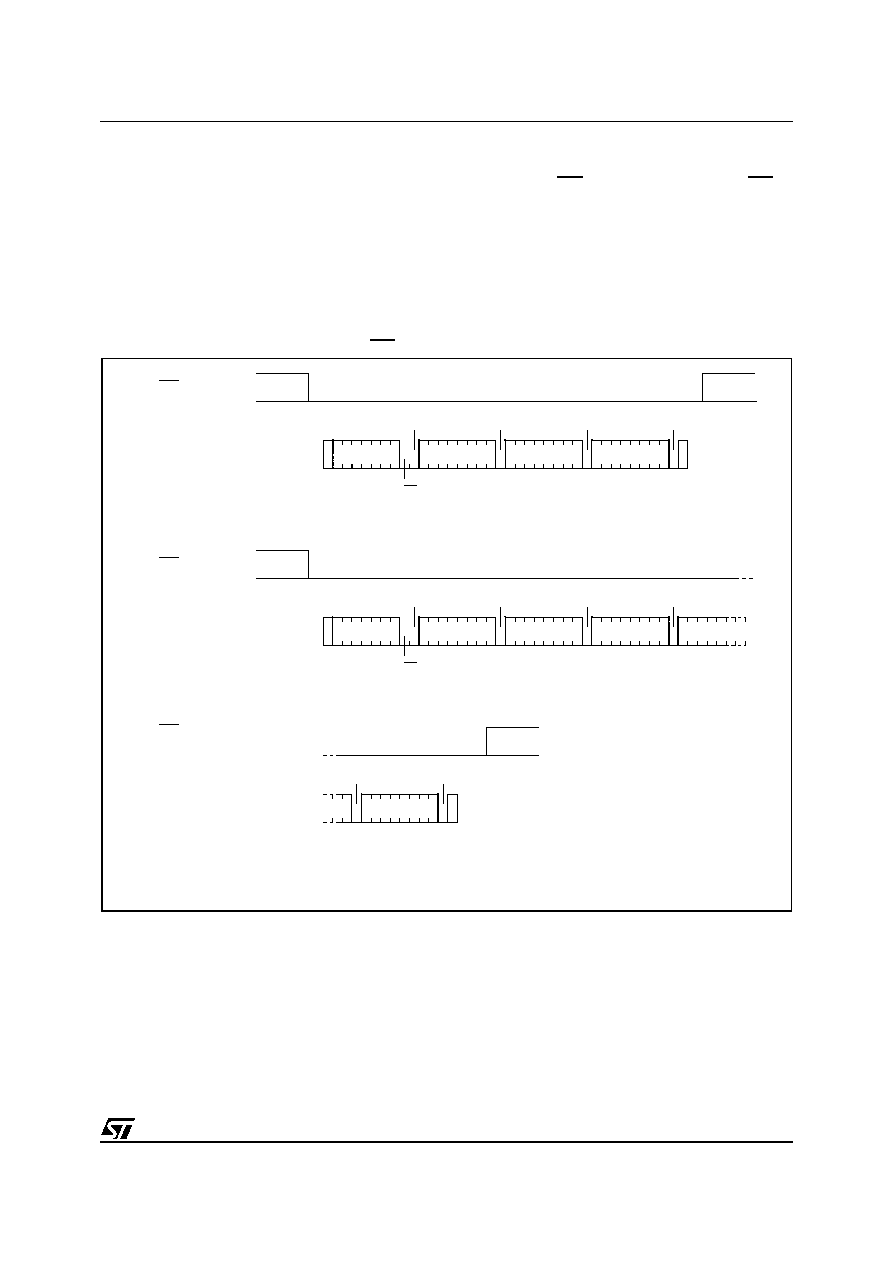
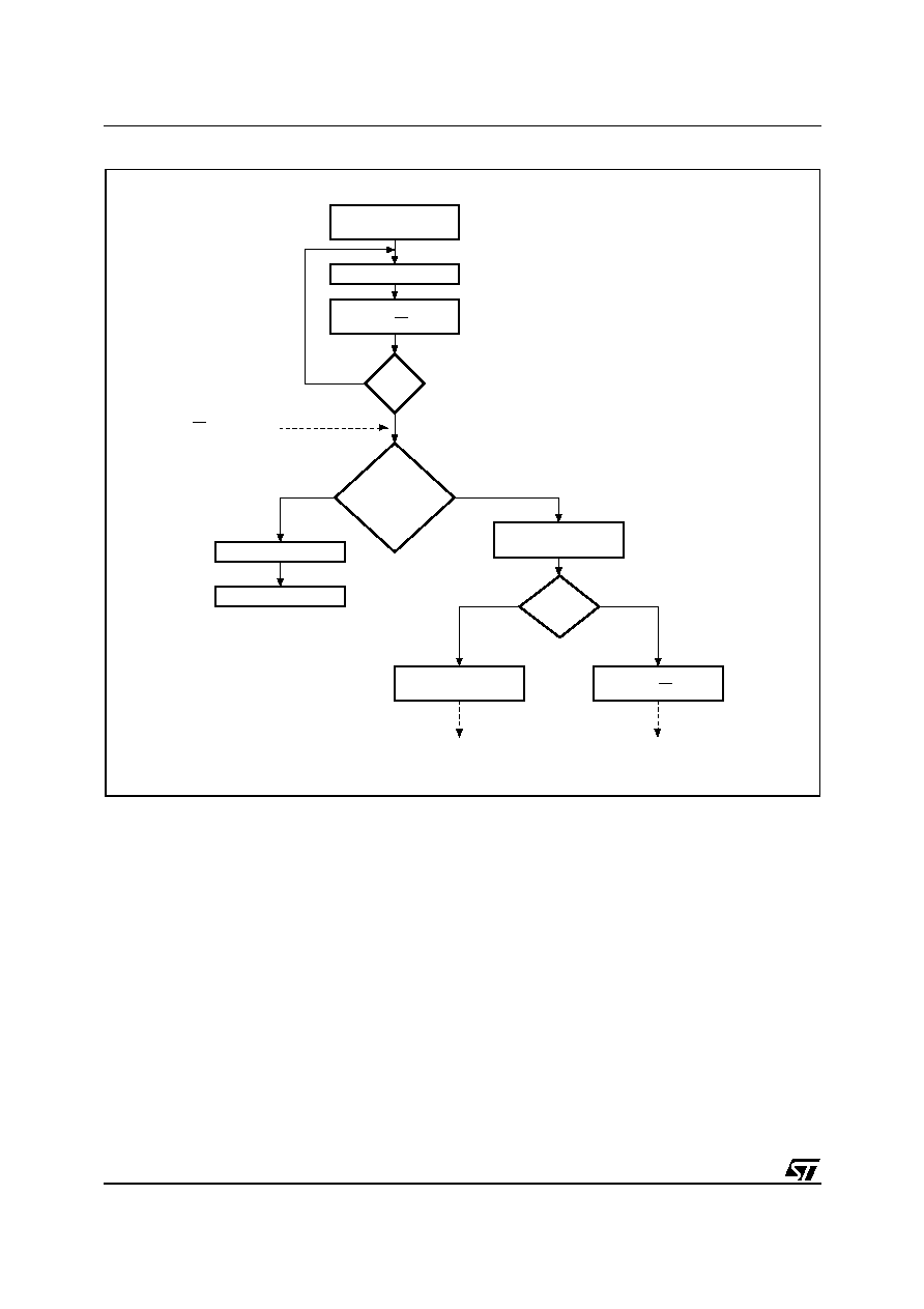
Figure 8. Write Cycle Polling Flowchart using ACK
Minimizing System Delays by Polling On ACK
During the internal Write cycle, the device discon-
nects itself from the bus, and writes a copy of the
data from its internal latches to the memory cells.
The maximum Write time (t
w
) is shown in Table
15, but the typical time is shorter. To make use of
this, a polling sequence can be used by the bus
master.
The sequence, as shown in Figure 8, is:
≠ Initial condition: a Write cycle is in progress.
≠ Step 1: the bus master issues a Start condition
followed by a Device Select Code (the first byte
of the new instruction).
≠ Step 2: if the device is busy with the internal
Write cycle, no Ack will be returned and the bus
master goes back to Step 1. If the device has
terminated the internal Write cycle, it responds
with an Ack, indicating that the device is ready
to receive the second part of the instruction (the
first byte of this instruction having been sent
during Step 1).
WRITE Cycle
in Progress
AI01847C
Next
Operation is
Addressing the
Memory
START Condition
DEVICE SELECT
with RW = 0
ACK
Returned
YES
NO
YES
NO
ReSTART
STOP
DATA for the
WRITE Operation
DEVICE SELECT
with RW = 1
Send Address
and Receive ACK
First byte of instruction
with RW = 0 already
decoded by the device
YES
NO
START
Condition
Continue the
WRITE Operation
Continue the
Random READ Operation
11/24
M24512
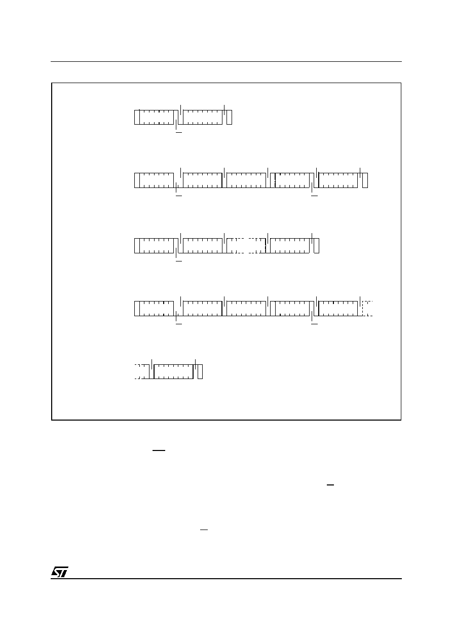
Figure 9. Read Mode Sequences
Note: 1. The seven most significant bits of the Device Select Code of a Random Read (in the 1
st
and 4
th
bytes) must be identical.
Read Operations
Read operations are performed independently of
the state of the Write Control (WC) signal.
After the successful completion of a Read opera-
tion, the device's internal address counter is incre-
mented by one, to point to the next byte address.
Random Address Read
A dummy Write is first performed to load the ad-
dress into this address counter (as shown in Fig-
ure 9) but
without
sending a Stop condition. Then,
the bus master sends another Start condition, and
repeats the Device Select Code, with the RW bit
set to 1. The device acknowledges this, and out-
puts the contents of the addressed byte. The bus
master must
not
acknowledge the byte, and termi-
nates the transfer with a Stop condition.
Current Address Read
For the Current Address Read operation, following
a Start condition, the bus master only sends a De-
vice Select Code with the RW bit set to 1. The de-
vice acknowledges this, and outputs the byte
addressed by the internal address counter. The
counter is then incremented. The bus master ter-
minates the transfer with a Stop condition, as
shown in Figure 9,
without
acknowledging the
byte.
START
DEV SEL *
BYTE ADDR
BYTE ADDR
START
DEV SEL
DATA OUT 1
AI01105C
DATA OUT N
STOP
START
CURRENT
ADDRESS
READ
DEV SEL
DATA OUT
RANDOM
ADDRESS
READ
STOP
START
DEV SEL *
DATA OUT
SEQUENTIAL
CURRENT
READ
STOP
DATA OUT N
START
DEV SEL *
BYTE ADDR
BYTE ADDR
SEQUENTIAL
RANDOM
READ
START
DEV SEL *
DATA OUT 1
STOP
ACK
R/W
NO ACK
ACK
R/W
ACK
ACK
ACK
R/W
ACK
ACK
ACK
NO ACK
R/W
NO ACK
ACK
ACK
ACK
R/W
ACK
ACK
R/W
ACK
NO ACK

M24512
12/24
Sequential Read
This operation can be used after a Current Ad-
dress Read or a Random Address Read. The bus
master
does
acknowledge the data byte output,
and sends additional clock pulses so that the de-
vice continues to output the next byte in sequence.
To terminate the stream of bytes, the bus master
must
not
acknowledge the last byte, and
must
generate a Stop condition, as shown in Figure 9.
The output data comes from consecutive address-
es, with the internal address counter automatically
incremented after each byte output. After the last
memory address, the address counter `rolls-over',
and the device continues to output data from
memory address 00h.
Acknowledge in Read Mode
For all Read commands, the device waits, after
each byte read, for an acknowledgment during the
9
th
bit time. If the bus master does not drive Serial
Data (SDA) Low during this time, the device termi-
nates the data transfer and switches to its Stand-
by mode.
INITIAL DELIVERY STATE
The device is delivered with the memory array
erased: all bits are set to 1 (each byte contains
FFh).
13/24
M24512
MAXIMUM RATING
Stressing the device above the rating listed in the
Absolute Maximum Ratings" table may cause per-
manent damage to the device. These are stress
ratings only and operation of the device at these or
any other conditions above those indicated in the
Operating sections of this specification is not im-
plied. Exposure to Absolute Maximum Rating con-
ditions for extended periods may affect device
reliability. Refer also to the STMicroelectronics
SURE Program and other relevant quality docu-
ments.
Table 6. Absolute Maximum Ratings
Note: 1. Compliant with the ECOPACK
Æ
7191395 specifiication for lead-free soldering processes
2. No longer than 10 seconds
3. Not exceeding 250∞C for more than 30 seconds, and peaking at 260∞C
4. JEDEC Std JESD22-A114A (C1=100 pF, R1=1500
, R2=500
)
Symbol
Parameter
Min.
Max.
Unit
T
A
Ambient Operating Temperature
≠40
125
∞C
T
STG
Storage Temperature
≠65
150
∞C
T
LEAD
Lead Temperature during Soldering
1
PDIP
SO
LGA
260
2
260
3
260
3
∞C
V
IO
Input or Output range
≠0.6
6.5
V
V
CC
Supply Voltage
≠0.3
6.5
V
V
ESD
Electrostatic Discharge Voltage (Human Body model)
4
≠4000
4000
V

M24512
14/24
DC AND AC PARAMETERS
This section summarizes the operating and mea-
surement conditions, and the DC and AC charac-
teristics of the device. The parameters in the DC
and AC Characteristic tables that follow are de-
rived from tests performed under the Measure-
ment Conditions summarized in the relevant
tables. Designers should check that the operating
conditions in their circuit match the measurement
conditions when relying on the quoted parame-
ters.
Table 7. Operating Conditions (M24512)
Table 8. Operating Conditions (M24512-W)
Table 9. Operating Conditions (M24512-S)
Table 10. AC Measurement Conditions
Figure 10. AC Measurement I/O Waveform
Symbol
Parameter
Min.
Max.
Unit
V
CC
Supply Voltage
4.5
5.5
V
T
A
Ambient Operating Temperature
≠40
85
∞C
≠20
85
∞C
Symbol
Parameter
Min.
Max.
Unit
V
CC
Supply Voltage
2.5
5.5
V
T
A
Ambient Operating Temperature
≠40
85
∞C
≠20
85
∞C
Symbol
Parameter
Min.
Max.
Unit
V
CC
Supply Voltage
1.8
3.6
V
T
A
Ambient Operating Temperature
≠20
85
∞C
Symbol
Parameter
Min.
Max.
Unit
C
L
Load Capacitance
100
pF
Input Rise and Fall Times
50
ns
Input Levels
0.2V
CC
to 0.8V
CC
V
Input and Output Timing Reference Levels
0.3V
CC
to 0.7V
CC
V
AI00825B
0.8VCC
0.2VCC
0.7VCC
0.3VCC
Input and Output
Timing Reference Levels
Input Levels

15/24
M24512
Table 11. Input Parameters
Note: 1. T
A
= 25 ∞C, f = 400 kHz
2. Sampled only, not 100% tested.
Table 12. DC Characteristics (M24512)
Table 13. DC Characteristics (M24512-W)
Symbol
Parameter
1,2
Test Condition
Min
.
Max
.
Unit
C
IN
Input Capacitance (SDA)
8
pF
C
IN
Input Capacitance (other pins)
6
pF
Z
L
Input Impedance
(E2, E1, E0, WC)
V
IN
< 0.5 V
30
k
Z
H
Input Impedance
(E2, E1, E0, WC)
V
IN
> 0.7V
CC
500
k
t
NS
Pulse width ignored
(Input Filter on SCL and SDA)
Single glitch
100
ns
Symbol
Parameter
Test Condition
(in addition to those in Table 7)
Min.
Max.
Unit
I
LI
Input Leakage Current
(SCL, SDA)
V
IN
= V
SS
or
V
CC
device in Stand-by mode
± 2
µA
I
LO
Output Leakage Current
V
OUT
= V
SS
or
V
CC,
SDA in Hi-Z
± 2
µA
I
CC
Supply Current
V
CC
=5V, f
c
=400kHz (rise/fall time < 30ns)
2
mA
I
CC1
Stand-by Supply Current
V
IN
= V
SS
or
V
CC
, V
CC
= 5 V
10
µA
V
IL
Input Low Voltage (SCL, SDA)
≠0.45
0.3V
CC
V
Input Low Voltage
(E2, E1, E0, WC)
≠0.45
0.5
V
V
IH
Input High Voltage
(E2, E1, E0, SCL, SDA, WC)
0.7V
CC
V
CC
+1
V
V
OL
Output Low Voltage
I
OL
= 3 mA, V
CC
= 5 V
0.4
V
Symbol
Parameter
Test Condition
(in addition to those in Table 8)
Min.
Max.
Unit
I
LI
Input Leakage Current
(SCL, SDA)
V
IN
= V
SS
or
V
CC
device in Stand-by mode
± 2
µA
I
LO
Output Leakage Current
V
OUT
= V
SS
or
V
CC,
SDA in Hi-Z
± 2
µA
I
CC
Supply Current
V
CC
=2.5V, f
c
=400kHz (rise/fall time < 30ns)
1
mA
I
CC1
Stand-by Supply Current
V
IN
= V
SS
or
V
CC
, V
CC
= 2.5 V
2
µA
V
IL
Input Low Voltage (SCL, SDA)
≠0.45
0.3V
CC
V
Input Low Voltage
(E2, E1, E0, WC)
≠0.45
0.5
V
V
IH
Input High Voltage
(E2, E1, E0, SCL, SDA, WC)
0.7V
CC
V
CC
+1
V
V
OL
Output Low Voltage
I
OL
= 2.1 mA, V
CC
= 2.5 V
0.4
V

M24512
16/24
Table 14. DC Characteristics (M24512-S)
Note: 1. Preliminary data
Symbol
Parameter
Test Condition
(in addition to those in Table 9)
Min.
Max.
Unit
I
LI
Input Leakage Current
(SCL, SDA)
V
IN
= V
SS
or
V
CC
device in Stand-by mode
± 2
µA
I
LO
Output Leakage Current
V
OUT
= V
SS
or
V
CC,
SDA in Hi-Z
± 2
µA
I
CC
Supply Current
V
CC
=1.8V, f
c
=400kHz (rise/fall time < 30ns)
0.8
1
mA
I
CC1
Stand-by Supply Current
V
IN
= V
SS
or
V
CC
, V
CC
= 1.8 V
1
1
µA
V
IL
Input Low Voltage (SCL, SDA)
≠0.45
0.3 V
CC
V
Input Low Voltage
(E2, E1, E0, WC)
≠0.45
0.5
V
V
IH
Input High Voltage
(E2, E1, E0, SCL, SDA, WC)
0.7V
CC
V
CC
+0.6
V
V
OL
Output Low Voltage
I
OL
= 0.7 mA, V
CC
= 1.8 V
0.2
1
V
17/24
M24512
Table 15. AC Characteristics
Note: 1. For a reSTART condition, or following a Write cycle.
2. Sampled only, not 100% tested.
3. To avoid spurious START and STOP conditions, a minimum delay is placed between SCL=1 and the falling or rising edge of SDA.
4. For the M24512-S, this is preliminary data
Test conditions specified in Table 10 and Table 7 or 8 or 9
Symbol
Alt.
Parameter
Min.
4
Max.
4
Unit
f
C
f
SCL
Clock Frequency
400
kHz
t
CHCL
t
HIGH
Clock Pulse Width High
600
ns
t
CLCH
t
LOW
Clock Pulse Width Low
1300
ns
t
CH1CH2
t
R
Clock Rise Time
300
ns
t
CL1CL2
t
F
Clock Fall Time
300
ns
t
DH1DH2
2
t
R
SDA Rise Time
20
300
ns
t
DL1DL2
2
t
F
SDA Fall Time
20
300
ns
t
DXCX
t
SU:DAT
Data In Set Up Time
100
ns
t
CLDX
t
HD:DAT
Data In Hold Time
0
ns
t
CLQX
t
DH
Data Out Hold Time
200
ns
t
CLQV
3
t
AA
Clock Low to Next Data Valid (Access Time)
200
900
ns
t
CHDX
1
t
SU:STA
Start Condition Set Up Time
600
ns
t
DLCL
t
HD:STA
Start Condition Hold Time
600
ns
t
CHDH
t
SU:STO
Stop Condition Set Up Time
600
ns
t
DHDL
t
BUF
Time between Stop Condition and Next Start
Condition
1300
ns
t
W
t
WR
Write Time
10
ms

M24512
18/24
Figure 11. AC Waveforms
SCL
SDA In
SCL
SDA Out
SCL
SDA In
tCHCL
tDLCL
tCHDX
START
Condition
tCLCH
tDXCX
tCLDX
SDA
Input
SDA
Change
tCHDH
tDHDL
STOP
Condition
Data Valid
tCLQV
tCLQX
tCHDH
STOP
Condition
tCHDX
START
Condition
Write Cycle
tW
AI00795C
START
Condition
19/24
M24512
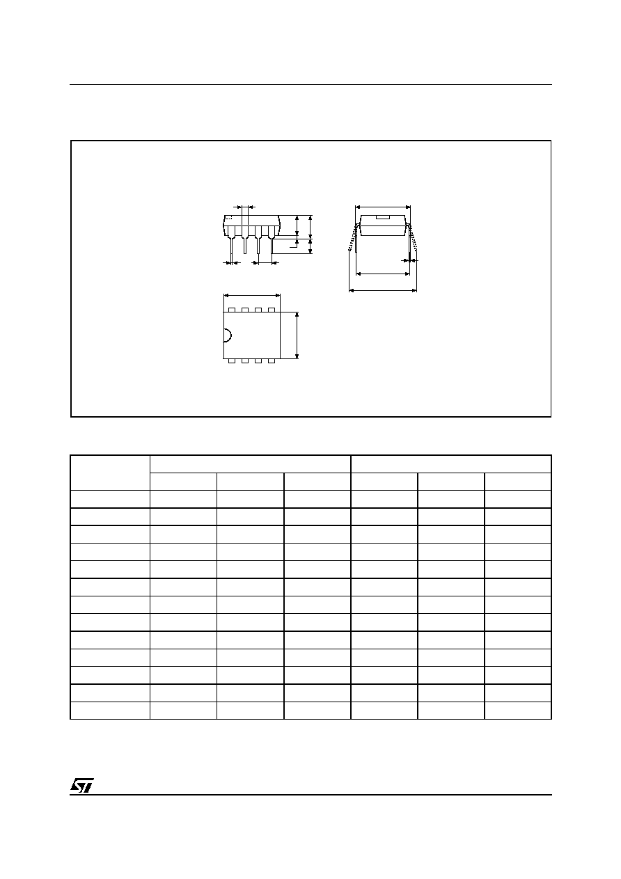
PACKAGE MECHANICAL
Figure 12. PDIP8 ≠ 8 pin Plastic DIP, 0.25mm lead frame, Package Outline
Notes: 1. Drawing is not to scale.
Table 16. PDIP8 ≠ 8 pin Plastic DIP, 0.25mm lead frame, Package Mechanical Data
PDIP-B
A2
A1
A
L
b
e
D
E1
8
1
c
eA
b2
eB
E
Symb.
mm
inches
Typ.
Min.
Max.
Typ.
Min.
Max.
A
5.33
0.210
A1
0.38
0.015
A2
3.30
2.92
4.95
0.130
0.115
0.195
b
0.46
0.36
0.56
0.018
0.014
0.022
b2
1.52
1.14
1.78
0.060
0.045
0.070
c
0.25
0.20
0.36
0.010
0.008
0.014
D
9.27
9.02
10.16
0.365
0.355
0.400
E
7.87
7.62
8.26
0.310
0.300
0.325
E1
6.35
6.10
7.11
0.250
0.240
0.280
e
2.54
≠
≠
0.100
≠
≠
eA
7.62
≠
≠
0.300
≠
≠
eB
10.92
0.430
L
3.30
2.92
3.81
0.130
0.115
0.150
M24512
20/24
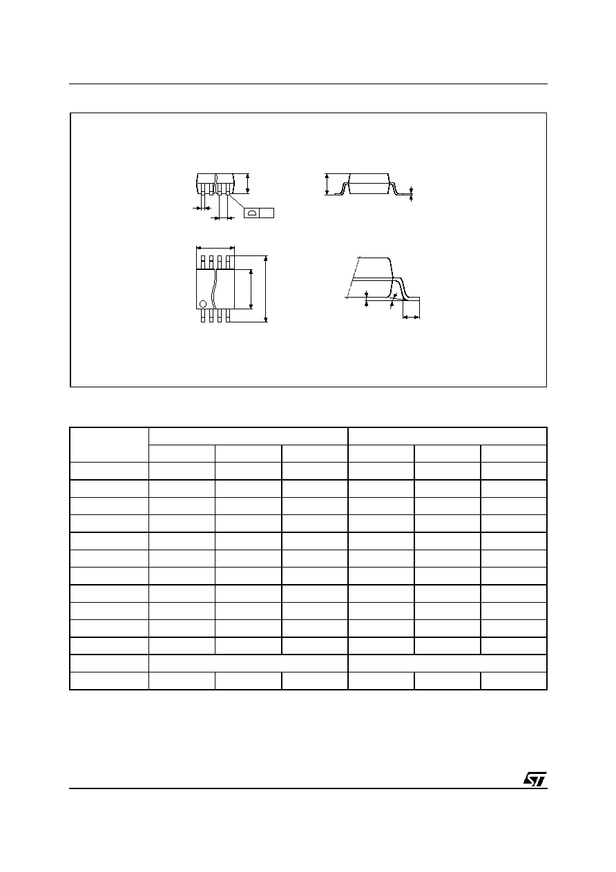
Figure 13. SO8 wide ≠ 8 lead Plastic Small Outline, 200 mils body width, Package Outline
Note: Drawing is not to scale.
Table 17. SO8 wide ≠ 8 lead Plastic Small Outline, 200 mils body width, Package Mechanical Data
Symb.
mm
inches
Typ.
Min.
Max.
Typ.
Min.
Max.
A
2.03
0.080
A1
0.10
0.25
0.004
0.010
A2
1.78
0.070
B
0.35
0.45
0.014
0.018
C
0.20
≠
≠
0.008
≠
≠
D
5.15
5.35
0.203
0.211
E
5.20
5.40
0.205
0.213
e
1.27
≠
≠
0.050
≠
≠
H
7.70
8.10
0.303
0.319
L
0.50
0.80
0.020
0.031
0∞
10∞
0∞
10∞
N
8
8
CP
0.10
0.004
SO-b
E
N
CP
B
e
A2
D
C
L
A1
H
A
1

21/24
M24512
Figure 14. LGA8 - 8 lead Land Grid Array, Package Outline
Notes: 1. Drawing is not to scale.
Table 18. LGA8 - 8 lead Land Grid Array, Package Mechanical Data
D
E
A2
A1
T1
T2
E2
E1
E3
T3
D1
LGA-Z01B
CONTACT 1
A
ddd
k
Symb.
mm
inches
Typ.
Min.
Max.
Typ.
Min.
Max.
A
1.040
0.940
1.140
0.0409
0.0370
0.0449
A1
0.340
0.300
0.380
0.0134
0.0118
0.0150
A2
0.700
0.640
0.760
0.0276
0.0252
0.0299
D
8.000
7.900
8.100
0.3150
0.3110
0.3189
D1
0.100
≠
≠
0.0039
≠
≠
E
5.000
4.900
5.100
0.1969
0.1929
0.2008
E1
1.270
≠
≠
0.0500
≠
≠
E2
3.810
≠
≠
0.1500
≠
≠
E3
0.390
≠
≠
0.0154
≠
≠
k
0.100
≠
≠
0.0039
≠
≠
T1
0.410
≠
≠
0.0161
≠
≠
T2
0.670
≠
≠
0.0264
≠
≠
T3
0.970
≠
≠
0.0382
≠
≠
ddd
0.100
≠
≠
0.0039
≠
≠

M24512
22/24
PART NUMBERING
Table 19. Ordering Information Scheme
Note: 1. The -S version (V
CC
range 1.8 V to 3.6 V) is only available in temperature range 5.
For a list of available options (speed, package,
etc.) or for further information on any aspect of this
device, please contact your nearest ST Sales Of-
fice.
Example:
M24512
≠
W MW 6
T
P
Device Type
M24 = I
2
C serial access EEPROM
Device Function
512 = 512 Kbit (64K x 8)
Operating Voltage
blank = V
CC
= 4.5 to 5.5V
W = V
CC
= 2.5 to 5.5V
S
1
= V
CC
= 1.8 to 3.6V
Package
BN = PDIP8
MW = SO8 (200 mil width)
LA = LGA8 (Land Grid Array)
Temperature Range
6 = ≠40 to 85 ∞C
5 = ≠20 to 85 ∞C
Option
blank = Standard Packing
T = Tape & Reel Packing
Plating Technology
blank = Standard SnPb plating
P = Pb-Free, RoHS compliant
G = Green package

23/24
M24512
REVISION HISTORY
Table 20. Document Revision History
Date
Rev.
Description of Revision
29-Jan-2001
1.1
Lead Soldering Temperature in the Absolute Maximum Ratings table amended
Write Cycle Polling Flow Chart using ACK illustration updated
LGA8 and SO8(wide) packages added
References to PSDIP8 changed to PDIP8, and Package Mechanical data updated
10-Apr-2001
1.2
LGA8 Package Mechanical data and illustration updated
SO16 package removed
16-Jul-2001
1.3
LGA8 Package given the designator "LA"
02-Oct-2001
1.4
LGA8 Package mechanical data updated
13-Dec-2001
1.5
Document becomes Preliminary Data
Test conditions for ILI, ILO, ZL and ZH made more precise
VIL and VIH values unified. tNS value changed
12-Jun-2001
1.6
Document becomes Full Datasheet
22-Oct-2003
4.0
Table of contents, and Pb-free options added. Minor wording changes in Summary
Description, Power-On Reset, Memory Addressing, Write Operations, Read Operations.
V
IL
(min) improved to -0.45V.

M24512
24/24
Information furnished is believed to be accurate and reliable. However, STMicroelectronics assumes no responsibility for the consequences
of use of such information nor for any infringement of patents or other rights of third parties which may result from its use. No license is granted
by implication or otherwise under any patent or patent rights of STMicroelectronics. Specifications mentioned in this publication are subject
to change without notice. This publication supersedes and replaces all information previously supplied. STMicroelectronics products are not
authorized for use as critical components in life support devices or systems without express written approval of STMicroelectronics.
The ST logo is a registered trademark of STMicroelectronics.
All other names are the property of their respective owners
© 2003 STMicroelectronics - All rights reserved
STMicroelectronics GROUP OF COMPANIES
Australia - Belgium - Brazil - Canada - China - Czech Republic - Finland - France - Germany - Hong Kong - India - Israel - Italy - Japan -
Malaysia - Malta - Morocco - Singapore - Spain - Sweden - Switzerland - United Kingdom - United States
www.st.com