Document Outline
- FEATURES SUMMARY
- SIGNAL DESCRIPTION
- DEVICE OPERATION
- INITIAL DELIVERY STATE
- MAXIMUM RATING
- DC AND AC PARAMETERS
- PACKAGE MECHANICAL
- Figure 12. PDIP8 Ö 8 pin Plastic DIP, 0.25mm lead frame, Package Outline
- Table 16. PDIP8 Ö 8 pin Plastic DIP, 0.25mm lead frame, Package Mechanical Data
- Figure 13. SO8W Ö 8 lead Plastic Small Outline, 208 mils body width, Package Outline
- Table 17. SO8W Ö 8 lead Plastic Small Outline, 208 mils body width, Package Mechanical Data
- Figure 14. SO8N Ö 8 lead Plastic Small Outline, 150 mils body width, Package Outline
- Table 18. SO8N Ö 8 lead Plastic Small Outline, 150 mils body width, Package Mechanical Data
- Figure 15. TSSOP8 Ö 8 lead Thin Shrink Small Outline, Package Outline
- Table 19. TSSOP8 Ö 8 lead Thin Shrink Small Outline, Package Mechanical Data
- PART NUMBERING
- REVISION HISTORY
1/24
February 2005
M24512
512 Kbit Serial I≤C Bus EEPROM
FEATURES SUMMARY
Two-Wire I
2
C Serial Interface
Supports 400 kHz Protocol
Supply Voltage Ranges:
≠
1.8V to 5.5V (M24512
-
R)
≠
2.5V to 5.5V (M24512
-
W)
Write Control Input
BYTE and PAGE WRITE (up to 128 Bytes)
RANDOM and SEQUENTIAL READ Modes
Self-Timed Programming Cycle
Automatic Address Incrementing
Enhanced ESD/Latch-Up Protection
More than 100,000 Erase/Write Cycles
More than 40-Year Data Retention
Table 1. M24512 devices
Figure 1. Packages
Reference
Part Number
M24512
M24512
-
W
M24512
-
R
PDIP8 (BN)
8
1
SO8 (MW)
208 mil width
TSSOP8 (DW)
8
1
8
1
SO8 (MN)
150 mil width

M24512
2/24
TABLE OF CONTENTS
FEATURES SUMMARY . . . . . . . . . . . . . . . . . . . . . . . . . . . . . . . . . . . . . . . . . . . . . . . . . . . . . . . . . . . . . 1
Table 1. M24512 devices. . . . . . . . . . . . . . . . . . . . . . . . . . . . . . . . . . . . . . . . . . . . . . . . . . . . . . . . . 1
Figure 1. Packages . . . . . . . . . . . . . . . . . . . . . . . . . . . . . . . . . . . . . . . . . . . . . . . . . . . . . . . . . . . . . . 1
Figure 2. Logic Diagram . . . . . . . . . . . . . . . . . . . . . . . . . . . . . . . . . . . . . . . . . . . . . . . . . . . . . . . . . . 4
Table 2. Signal Names . . . . . . . . . . . . . . . . . . . . . . . . . . . . . . . . . . . . . . . . . . . . . . . . . . . . . . . . . . 4
Power On Reset . . . . . . . . . . . . . . . . . . . . . . . . . . . . . . . . . . . . . . . . . . . . . . . . . . . . . . . . . . . . . . . . 4
Figure 3. DIP, SO and TSSOP Connections . . . . . . . . . . . . . . . . . . . . . . . . . . . . . . . . . . . . . . . . . . 4
SIGNAL DESCRIPTION . . . . . . . . . . . . . . . . . . . . . . . . . . . . . . . . . . . . . . . . . . . . . . . . . . . . . . . . . . . . . 5
Serial Clock (SCL) . . . . . . . . . . . . . . . . . . . . . . . . . . . . . . . . . . . . . . . . . . . . . . . . . . . . . . . . . . . . . . . 5
Serial Data (SDA) . . . . . . . . . . . . . . . . . . . . . . . . . . . . . . . . . . . . . . . . . . . . . . . . . . . . . . . . . . . . . . . 5
Chip Enable (E0, E1, E2) . . . . . . . . . . . . . . . . . . . . . . . . . . . . . . . . . . . . . . . . . . . . . . . . . . . . . . . . . 5
Write Control (WC) . . . . . . . . . . . . . . . . . . . . . . . . . . . . . . . . . . . . . . . . . . . . . . . . . . . . . . . . . . . . . . 5
Figure 4. Maximum R
P
Value versus Bus Parasitic Capacitance (C) for an I
2
C Bus . . . . . . . . . . . . 5
Figure 5. I
2
C Bus Protocol . . . . . . . . . . . . . . . . . . . . . . . . . . . . . . . . . . . . . . . . . . . . . . . . . . . . . . . . 6
Table 3. Device Select Code . . . . . . . . . . . . . . . . . . . . . . . . . . . . . . . . . . . . . . . . . . . . . . . . . . . . . . 6
Table 4. Most Significant Byte . . . . . . . . . . . . . . . . . . . . . . . . . . . . . . . . . . . . . . . . . . . . . . . . . . . . . 6
Table 5. Least Significant Byte . . . . . . . . . . . . . . . . . . . . . . . . . . . . . . . . . . . . . . . . . . . . . . . . . . . . 6
DEVICE OPERATION . . . . . . . . . . . . . . . . . . . . . . . . . . . . . . . . . . . . . . . . . . . . . . . . . . . . . . . . . . . . . . . 7
Start Condition. . . . . . . . . . . . . . . . . . . . . . . . . . . . . . . . . . . . . . . . . . . . . . . . . . . . . . . . . . . . . . . . . 7
Stop Condition . . . . . . . . . . . . . . . . . . . . . . . . . . . . . . . . . . . . . . . . . . . . . . . . . . . . . . . . . . . . . . . . . 7
Acknowledge Bit (ACK) . . . . . . . . . . . . . . . . . . . . . . . . . . . . . . . . . . . . . . . . . . . . . . . . . . . . . . . . . 7
Data Input . . . . . . . . . . . . . . . . . . . . . . . . . . . . . . . . . . . . . . . . . . . . . . . . . . . . . . . . . . . . . . . . . . . . . 7
Memory Addressing . . . . . . . . . . . . . . . . . . . . . . . . . . . . . . . . . . . . . . . . . . . . . . . . . . . . . . . . . . . . 7
Table 6. Operating Modes . . . . . . . . . . . . . . . . . . . . . . . . . . . . . . . . . . . . . . . . . . . . . . . . . . . . . . . . 7
Figure 6. Write Mode Sequences with WC=1 (data write inhibited) . . . . . . . . . . . . . . . . . . . . . . . . . 8
Write Operations . . . . . . . . . . . . . . . . . . . . . . . . . . . . . . . . . . . . . . . . . . . . . . . . . . . . . . . . . . . . . . . 8
Byte Write . . . . . . . . . . . . . . . . . . . . . . . . . . . . . . . . . . . . . . . . . . . . . . . . . . . . . . . . . . . . . . . . . . . . . 8
Page Write . . . . . . . . . . . . . . . . . . . . . . . . . . . . . . . . . . . . . . . . . . . . . . . . . . . . . . . . . . . . . . . . . . . . 9
Figure 7. Write Mode Sequences with WC=0 (data write enabled) . . . . . . . . . . . . . . . . . . . . . . . . . 9
Figure 8. Write Cycle Polling Flowchart using ACK . . . . . . . . . . . . . . . . . . . . . . . . . . . . . . . . . . . . 10
Minimizing System Delays by Polling On ACK. . . . . . . . . . . . . . . . . . . . . . . . . . . . . . . . . . . . . . 10
Figure 9. Read Mode Sequences . . . . . . . . . . . . . . . . . . . . . . . . . . . . . . . . . . . . . . . . . . . . . . . . . . 11
Read Operations . . . . . . . . . . . . . . . . . . . . . . . . . . . . . . . . . . . . . . . . . . . . . . . . . . . . . . . . . . . . . . 11
Random Address Read . . . . . . . . . . . . . . . . . . . . . . . . . . . . . . . . . . . . . . . . . . . . . . . . . . . . . . . . . 11
Current Address Read . . . . . . . . . . . . . . . . . . . . . . . . . . . . . . . . . . . . . . . . . . . . . . . . . . . . . . . . . 11
Sequential Read. . . . . . . . . . . . . . . . . . . . . . . . . . . . . . . . . . . . . . . . . . . . . . . . . . . . . . . . . . . . . . . 12
Acknowledge in Read Mode . . . . . . . . . . . . . . . . . . . . . . . . . . . . . . . . . . . . . . . . . . . . . . . . . . . . . 12
INITIAL DELIVERY STATE. . . . . . . . . . . . . . . . . . . . . . . . . . . . . . . . . . . . . . . . . . . . . . . . . . . . . . . . . . 12
MAXIMUM RATING. . . . . . . . . . . . . . . . . . . . . . . . . . . . . . . . . . . . . . . . . . . . . . . . . . . . . . . . . . . . . . . . 13
Table 7. Absolute Maximum Ratings . . . . . . . . . . . . . . . . . . . . . . . . . . . . . . . . . . . . . . . . . . . . . . . 13

3/24
M24512
DC AND AC PARAMETERS. . . . . . . . . . . . . . . . . . . . . . . . . . . . . . . . . . . . . . . . . . . . . . . . . . . . . . . . . 14
Table 8. Operating Conditions (M24512 ≠ W) . . . . . . . . . . . . . . . . . . . . . . . . . . . . . . . . . . . . . . . . 14
Table 9. Operating Conditions (M24512 ≠ R) . . . . . . . . . . . . . . . . . . . . . . . . . . . . . . . . . . . . . . . . 14
Table 10. AC Measurement Conditions. . . . . . . . . . . . . . . . . . . . . . . . . . . . . . . . . . . . . . . . . . . . . . 14
Figure 10.AC Measurement I/O Waveform . . . . . . . . . . . . . . . . . . . . . . . . . . . . . . . . . . . . . . . . . . . 14
Table 11. Input Parameters . . . . . . . . . . . . . . . . . . . . . . . . . . . . . . . . . . . . . . . . . . . . . . . . . . . . . . . 15
Table 12. DC Characteristics (M24512 ≠ W) . . . . . . . . . . . . . . . . . . . . . . . . . . . . . . . . . . . . . . . . . . 15
Table 13. DC Characteristics
(1)
(M24512 ≠ R) . . . . . . . . . . . . . . . . . . . . . . . . . . . . . . . . . . . . . . . . 15
Table 14. AC Characteristics (M24512 ≠ W) . . . . . . . . . . . . . . . . . . . . . . . . . . . . . . . . . . . . . . . . . . 16
Table 15. AC Characteristics
(1)
(M24512 ≠ R) . . . . . . . . . . . . . . . . . . . . . . . . . . . . . . . . . . . . . . . . 16
Figure 11.AC Waveforms . . . . . . . . . . . . . . . . . . . . . . . . . . . . . . . . . . . . . . . . . . . . . . . . . . . . . . . . 17
PACKAGE MECHANICAL . . . . . . . . . . . . . . . . . . . . . . . . . . . . . . . . . . . . . . . . . . . . . . . . . . . . . . . . . . 18
Figure 12.PDIP8 ≠ 8 pin Plastic DIP, 0.25mm lead frame, Package Outline . . . . . . . . . . . . . . . . . 18
Table 16. PDIP8 ≠ 8 pin Plastic DIP, 0.25mm lead frame, Package Mechanical Data . . . . . . . . . . 18
Figure 13.SO8W ≠ 8 lead Plastic Small Outline, 208 mils body width, Package Outline . . . . . . . . 19
Table 17. SO8W ≠ 8 lead Plastic Small Outline, 208 mils body width, Package Mechanical Data . 19
Figure 14.SO8N ≠ 8 lead Plastic Small Outline, 150 mils body width, Package Outline . . . . . . . . . 20
Table 18. SO8N ≠ 8 lead Plastic Small Outline, 150 mils body width, Package Mechanical Data . 20
Figure 15.TSSOP8 ≠ 8 lead Thin Shrink Small Outline, Package Outline . . . . . . . . . . . . . . . . . . . 21
Table 19. TSSOP8 ≠ 8 lead Thin Shrink Small Outline, Package Mechanical Data . . . . . . . . . . . . 21
PART NUMBERING . . . . . . . . . . . . . . . . . . . . . . . . . . . . . . . . . . . . . . . . . . . . . . . . . . . . . . . . . . . . . . . 22
Table 20. Ordering Information Scheme . . . . . . . . . . . . . . . . . . . . . . . . . . . . . . . . . . . . . . . . . . . . . 22
REVISION HISTORY . . . . . . . . . . . . . . . . . . . . . . . . . . . . . . . . . . . . . . . . . . . . . . . . . . . . . . . . . . . . . . . 23
Table 21. Document Revision History . . . . . . . . . . . . . . . . . . . . . . . . . . . . . . . . . . . . . . . . . . . . . . . 23
M24512
4/24
SUMMARY DESCRIPTION
These I
2
C-compatible electrically erasable pro-
grammable memory (EEPROM) devices are orga-
nized as 64K x 8 bits.
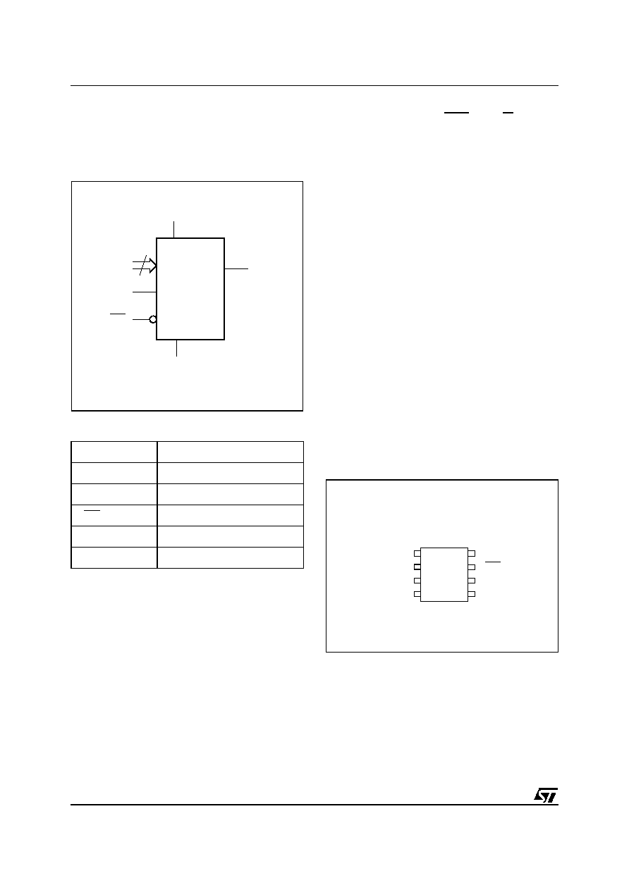
Figure 2. Logic Diagram
Table 2. Signal Names
I
2
C uses a two-wire serial interface, comprising a
bi-directional data line and a clock line. The devic-
es carry a built-in 4-bit Device Type Identifier code
(1010) in accordance with the I
2
C bus definition.
The device behaves as a slave in the I
2
C protocol,
with all memory operations synchronized by the
serial clock. Read and Write operations are initiat-
ed by a Start condition, generated by the bus mas-
ter. The Start condition is followed by a Device
Select Code and Read/Write bit (RW) (as de-
scribed in
Table 3.
), terminated by an acknowl-
edge bit.
When writing data to the memory, the device in-
serts an acknowledge bit during the 9
th
bit time,
following the bus master's 8-bit transmission.
When data is read by the bus master, the bus
master acknowledges the receipt of the data byte
in the same way. Data transfers are terminated by
a Stop condition after an Ack for Write, and after a
NoAck for Read.
Power On Reset
In order to prevent data corruption and inadvertent
Write operations during Power-up, a Power On
Reset (POR) circuit is included. At Power-up, the
device will not respond to any command until V
CC
has reached the Power On Reset threshold volt-
age (this threshold is lower than the V
CC
min oper-
ating voltage defined in Tables
8
and
9
). In the
same way, as soon as V
CC
drops from the normal
operating voltage, below the Power On Reset
threshold voltage, the device stops to respond to
any command.
Prior to selecting and issuing commands to the
memory, a valid and stable V
CC
voltage must be
applied. This voltage must remain stable and valid
until the end of the transmission of the command
and, for a Write instruction, until the completion of
the internal write cycle (t
W
).
Figure 3. DIP, SO and TSSOP Connections
Note: See
PACKAGE MECHANICAL
section for package dimen-
sions, and how to identify pin-1.
E0, E1, E2
Chip Enable
SDA
Serial Data
SCL
Serial Clock
WC
Write Control
V
CC
Supply Voltage
V
SS
Ground
AI02275
SDA
VCC
M24512
WC
SCL
VSS
3
E0-E2
1
AI04035B
2
3
4
8
7
6
5
SDA
VSS
SCL
WC
E1
E0
VCC
E2
M24512
5/24
M24512
SIGNAL DESCRIPTION
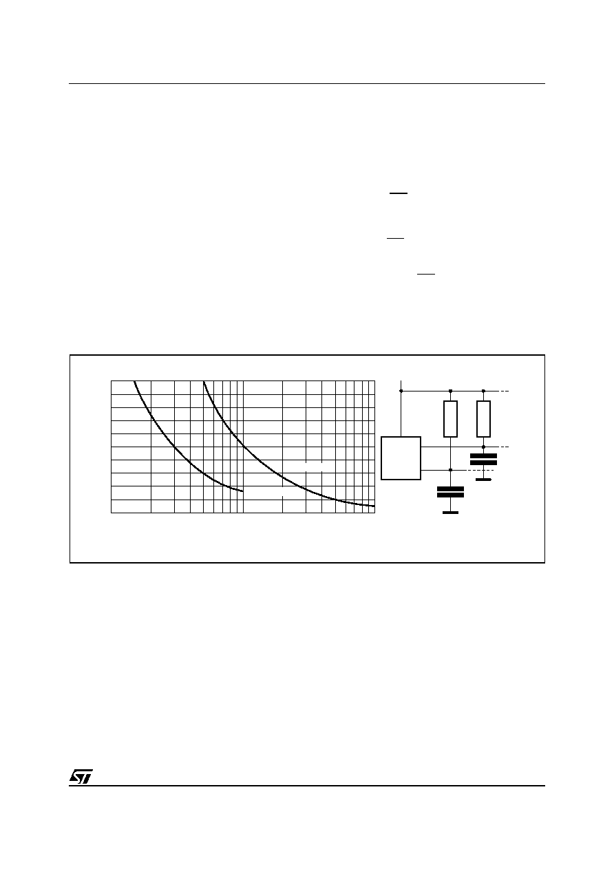
Serial Clock (SCL). This input signal is used to
strobe all data in and out of the device. In applica-
tions where this signal is used by slave devices to
synchronize the bus to a slower clock, the bus
master must have an open drain output, and a
pull-up resistor must be connected from Serial
Clock (SCL) to V
CC
. (
Figure 4.
indicates how the
value of the pull-up resistor can be calculated). In
most applications, though, this method of synchro-
nization is not employed, and so the pull-up resis-
tor is not necessary, provided that the bus master
has a push-pull (rather than open drain) output.
Serial Data (SDA). This bi-directional signal is
used to transfer data in or out of the device. It is an
open drain output that may be wire-OR'ed with
other open drain or open collector signals on the
bus. A pull up resistor must be connected from Se-
rial Data (SDA) to V
CC
. (
Figure 4.
indicates how
the value of the pull-up resistor can be calculated).
Chip Enable (E0, E1, E2). These input signals
are used to set the value that is to be looked for on
the three least significant bits (b3, b2, b1) of the 7-
bit Device Select Code. These inputs must be tied
to V
CC
or V
SS
, to establish the Device Select
Code. When not connected (left floating), these in-
puts are read as Low (0,0,0).
Write Control (WC). This input signal is useful
for protecting the entire contents of the memory
from inadvertent write operations. Write opera-
tions are disabled to the entire memory array when
Write Control (WC) is driven High. When uncon-
nected, the signal is internally read as V
IL
, and
Write operations are allowed.
When Write Control (WC) is driven High, Device
Select and Address bytes are acknowledged,
Data bytes are not acknowledged.
Figure 4. Maximum R
P
Value versus Bus Parasitic Capacitance (C) for an I
2
C Bus
AI01665b
VCC
C
SDA
R
P
MASTER
R
P
SCL
C
100
0
4
8
12
16
20
C (pF)
Maximum RP value (k
)
10
1000
fc = 400kHz
fc = 100kHz