Document Outline
- FEATURES SUMMARY
- SUMMARY DESCRIPTION
- SIGNAL DESCRIPTION
- DEVICE OPERATION
- INITIAL DELIVERY STATE
- MAXIMUM RATING
- DC and AC PARAMETERS
- PACKAGE MECHANICAL
- Figure 13. PDIP8 - 8 pin Plastic DIP, 0.25mm lead frame, Package Outline
- Table 15. PDIP8 - 8 pin Plastic DIP, 0.25mm lead frame, Package Mechanical Data
- Figure 14. SO8 narrow - 8 lead Plastic Small Outline, 150 mils body width, Package Outline
- Table 16. SO8 narrow - 8 lead Plastic Small Outline, 150 mils body width, Package Mechanical Data
- Figure 15. UFDFPN8 (MLP8) 8-lead Ultra thin Fine pitch Dual Flat Package No lead 2x3mm∑, Outline
- Table 17. UFDFPN8 (MLP8) 8-lead Ultra thin Fine pitch Dual Flat Package No lead 2x3mm∑, Data
- Figure 16. TSSOP8 - 8 lead Thin Shrink Small Outline, Package Outline
- Table 18. TSSOP8 - 8 lead Thin Shrink Small Outline, Package Mechanical Data
- Figure 17. TSSOP8 3x3mm∑ - 8 lead Thin Shrink Small Outline, 3x3mm∑ body size, Package Outline
- Table 19. TSSOP8 3x3mm∑ - 8 lead Thin Shrink Small Outline, 3x3mm∑ body size, Mechanical Data
- PART NUMBERING
- REVISION HISTORY
1/25
October 2005
M24C16, M24C08
M24C04, M24C02, M24C01
16Kbit, 8Kbit, 4Kbit, 2Kbit and 1Kbit Serial I≤C Bus EEPROM
FEATURES SUMMARY
Two-Wire I≤C Serial Interface
Supports 400kHz Protocol
Single Supply Voltage:
≠
2.5 to 5.5V for M24Cxx-W
≠
1.8 to 5.5V for M24Cxx-R
Write Control Input
BYTE and PAGE WRITE (up to 16 Bytes)
RANDOM and SEQUENTIAL READ Modes
Self-Timed Programming Cycle
Automatic Address Incrementing
Enhanced ESD/Latch-Up Protection
More than 1 Million Erase/Write Cycles
More than 40-Year Data Retention
Packages
≠
ECOPACKÆ (RoHS compliant)
Table 1. Product List
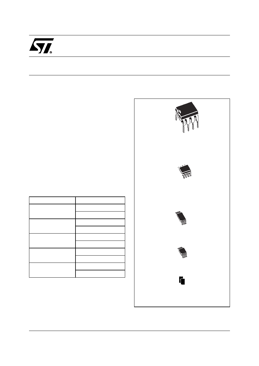
Figure 1. Packages
Reference
Part Number
M24C16
M24C16-W
M24C16-R
M24C08
M24C08-W
M24C08-R
M24C04
M24C04-W
M24C04-R
M24C02
M24C02-W
M24C02-R
M24C01
M24C01-W
M24C01-R
PDIP8 (BN)
SO8 (MN)
150 mil width
8
1
TSSOP8 (DW)
169 mil width
TSSOP8 (DS)
3x3mm≤ body size (MSOP)
8
1
UFDFPN8 (MB)
2x3mm≤ (MLP)

M24C16, M24C08, M24C04, M24C02, M24C01
2/25
TABLE OF CONTENTS
FEATURES SUMMARY . . . . . . . . . . . . . . . . . . . . . . . . . . . . . . . . . . . . . . . . . . . . . . . . . . . . . . . . . . . . . 1
SUMMARY DESCRIPTION . . . . . . . . . . . . . . . . . . . . . . . . . . . . . . . . . . . . . . . . . . . . . . . . . . . . . . . . . . . 3
Device internal reset . . . . . . . . . . . . . . . . . . . . . . . . . . . . . . . . . . . . . . . . . . . . . . . . . . . . . . . . . . . . 3
SIGNAL DESCRIPTION . . . . . . . . . . . . . . . . . . . . . . . . . . . . . . . . . . . . . . . . . . . . . . . . . . . . . . . . . . . . . 4
Serial Clock (SCL) . . . . . . . . . . . . . . . . . . . . . . . . . . . . . . . . . . . . . . . . . . . . . . . . . . . . . . . . . . . . . . . 4
Serial Data (SDA) . . . . . . . . . . . . . . . . . . . . . . . . . . . . . . . . . . . . . . . . . . . . . . . . . . . . . . . . . . . . . . . 4
Chip Enable (E0, E1, E2) . . . . . . . . . . . . . . . . . . . . . . . . . . . . . . . . . . . . . . . . . . . . . . . . . . . . . . . . . 4
Write Control (WC) . . . . . . . . . . . . . . . . . . . . . . . . . . . . . . . . . . . . . . . . . . . . . . . . . . . . . . . . . . . . . . 4
DEVICE OPERATION . . . . . . . . . . . . . . . . . . . . . . . . . . . . . . . . . . . . . . . . . . . . . . . . . . . . . . . . . . . . . . . 6
Start Condition. . . . . . . . . . . . . . . . . . . . . . . . . . . . . . . . . . . . . . . . . . . . . . . . . . . . . . . . . . . . . . . . . 6
Stop Condition . . . . . . . . . . . . . . . . . . . . . . . . . . . . . . . . . . . . . . . . . . . . . . . . . . . . . . . . . . . . . . . . . 6
Acknowledge Bit (ACK) . . . . . . . . . . . . . . . . . . . . . . . . . . . . . . . . . . . . . . . . . . . . . . . . . . . . . . . . . 6
Data Input . . . . . . . . . . . . . . . . . . . . . . . . . . . . . . . . . . . . . . . . . . . . . . . . . . . . . . . . . . . . . . . . . . . . . 6
Memory Addressing . . . . . . . . . . . . . . . . . . . . . . . . . . . . . . . . . . . . . . . . . . . . . . . . . . . . . . . . . . . . 6
Write Operations . . . . . . . . . . . . . . . . . . . . . . . . . . . . . . . . . . . . . . . . . . . . . . . . . . . . . . . . . . . . . . . 7
Byte Write . . . . . . . . . . . . . . . . . . . . . . . . . . . . . . . . . . . . . . . . . . . . . . . . . . . . . . . . . . . . . . . . . . . . . 7
Page Write . . . . . . . . . . . . . . . . . . . . . . . . . . . . . . . . . . . . . . . . . . . . . . . . . . . . . . . . . . . . . . . . . . . . 7
Minimizing System Delays by Polling On ACK. . . . . . . . . . . . . . . . . . . . . . . . . . . . . . . . . . . . . . . 9
Read Operations . . . . . . . . . . . . . . . . . . . . . . . . . . . . . . . . . . . . . . . . . . . . . . . . . . . . . . . . . . . . . . 10
Random Address Read . . . . . . . . . . . . . . . . . . . . . . . . . . . . . . . . . . . . . . . . . . . . . . . . . . . . . . . . . 10
Current Address Read . . . . . . . . . . . . . . . . . . . . . . . . . . . . . . . . . . . . . . . . . . . . . . . . . . . . . . . . . 10
Sequential Read. . . . . . . . . . . . . . . . . . . . . . . . . . . . . . . . . . . . . . . . . . . . . . . . . . . . . . . . . . . . . . . 11
Acknowledge in Read Mode . . . . . . . . . . . . . . . . . . . . . . . . . . . . . . . . . . . . . . . . . . . . . . . . . . . . . 11
INITIAL DELIVERY STATE. . . . . . . . . . . . . . . . . . . . . . . . . . . . . . . . . . . . . . . . . . . . . . . . . . . . . . . . . . 11
MAXIMUM RATING. . . . . . . . . . . . . . . . . . . . . . . . . . . . . . . . . . . . . . . . . . . . . . . . . . . . . . . . . . . . . . . . 12
DC and AC PARAMETERS . . . . . . . . . . . . . . . . . . . . . . . . . . . . . . . . . . . . . . . . . . . . . . . . . . . . . . . . . 13
PACKAGE MECHANICAL . . . . . . . . . . . . . . . . . . . . . . . . . . . . . . . . . . . . . . . . . . . . . . . . . . . . . . . . . . 18
PART NUMBERING . . . . . . . . . . . . . . . . . . . . . . . . . . . . . . . . . . . . . . . . . . . . . . . . . . . . . . . . . . . . . . . 23
REVISION HISTORY. . . . . . . . . . . . . . . . . . . . . . . . . . . . . . . . . . . . . . . . . . . . . . . . . . . . . . . . . . . . . . . 24
3/25
M24C16, M24C08, M24C04, M24C02, M24C01
SUMMARY DESCRIPTION
These I≤C-compatible electrically erasable pro-
grammable memory (EEPROM) devices are orga-
nized as 2048/1024/512/256/128 x 8 (M24C16,
M24C08, M24C04, M24C02 and M24C01).
In order to meet environmental requirements, ST
offers these devices in ECOPACKÆ packages.
ECOPACKÆ packages are Lead-free and RoHS
compliant.
ECOPACK is an ST trademark. ECOPACK speci-
fications are available at: www.st.com.
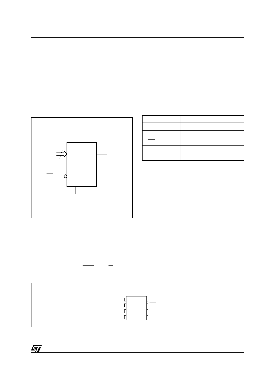
Figure 2. Logic Diagram
I≤C uses a two-wire serial interface, comprising a
bi-directional data line and a clock line. The devic-
es carry a built-in 4-bit Device Type Identifier code
(1010) in accordance with the I≤C bus definition.
The device behaves as a slave in the I≤C protocol,
with all memory operations synchronized by the
serial clock. Read and Write operations are initiat-
ed by a Start condition, generated by the bus mas-
ter. The Start condition is followed by a Device
Select Code and Read/Write bit (RW) (as de-
scribed in
Table 3.
), terminated by an acknowl-
edge bit.
When writing data to the memory, the device in-
serts an acknowledge bit during the 9
th
bit time,
following the bus master's 8-bit transmission.
When data is read by the bus master, the bus
master acknowledges the receipt of the data byte
in the same way. Data transfers are terminated by
a Stop condition after an Ack for Write, and after a
NoAck for Read.
Table 2. Signal Names
Device internal reset
In order to prevent inadvertent Write operations
during Power-up, a Power On Reset (POR) circuit
is included. At Power-up (continuous rise of V
CC
),
the device will not respond to any instructions until
the V
CC
has reached the Power On Reset
threshold voltage (this threshold is lower than the
V
CC
min. operating voltage defined in
DC and AC
PARAMETERS
). When V
CC
has passed over the
POR threshold, the device is reset and is in
Standby Power mode. At Power-down
(continuous decay of V
CC
), as soon as V
CC
drops
from the normal operating voltage to below the
Power On Reset threshold voltage, the device
stops responding to any instruction sent to it.
Prior to selecting and issuing instructions to the
memory, a valid and stable V
CC
voltage must be
applied. This voltage must remain stable and valid
until the end of the transmission of the instruction
and, for a Write instruction, until the completion of
the internal write cycle (t
W
).
Figure 3. 8-Pin Package Connections (Top View)
Note: 1. NC = Not Connected
2. See
PACKAGE MECHANICAL
section for package dimensions, and how to identify pin-1.
AI02033
3
E0-E2
SDA
VCC
M24Cxx
WC
SCL
VSS
E0, E1, E2
Chip Enable
SDA
Serial Data
SCL
Serial Clock
WC
Write Control
V
CC
Supply Voltage
V
SS
Ground
SDA
VSS
SCL
WC
VCC
/ E2
AI02034E
M24Cxx
1
2
3
4
8
7
6
5
/ E2
/ E2
/ E2
NC
/ E1
/ E1
/ E1
/ NC
NC
/ E0
/ E0
/ NC
/ NC
NC
/1Kb
/2Kb
/4Kb
/8Kb
16Kb
M24C16, M24C08, M24C04, M24C02, M24C01
4/25
SIGNAL DESCRIPTION
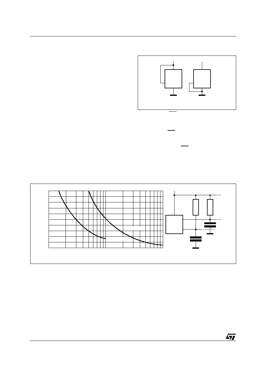
Serial Clock (SCL). This input signal is used to
strobe all data in and out of the device. In applica-
tions where this signal is used by slave devices to
synchronize the bus to a slower clock, the bus
master must have an open drain output, and a
pull-up resistor can be connected from Serial
Clock (SCL) to V
CC
. (
Figure 5.
indicates how the
value of the pull-up resistor can be calculated). In
most applications, though, this method of synchro-
nization is not employed, and so the pull-up resis-
tor is not necessary, provided that the bus master
has a push-pull (rather than open drain) output.
Serial Data (SDA). This bi-directional signal is
used to transfer data in or out of the device. It is an
open drain output that may be wire-OR'ed with
other open drain or open collector signals on the
bus. A pull up resistor must be connected from Se-
rial Data (SDA) to V
CC
. (
Figure 5.
indicates how
the value of the pull-up resistor can be calculated).
Chip Enable (E0, E1, E2). These input signals
are used to set the value that is to be looked for on
the three least significant bits (b3, b2, b1) of the 7-
bit Device Select Code. These inputs must be tied
to V
CC
or V
SS
, to establish the Device Select Code
as shown in
Figure 4.
Figure 4. Device Select Code
Write Control (WC). This input signal is useful
for protecting the entire contents of the memory
from inadvertent write operations. Write opera-
tions are disabled to the entire memory array when
Write Control (WC) is driven High. When uncon-
nected, the signal is internally read as V
IL
, and
Write operations are allowed.
When Write Control (WC) is driven High, Device
Select and Address bytes are acknowledged,
Data bytes are not acknowledged.
Figure 5. Maximum RP Value versus Bus Parasitic Capacitance (C) for an I≤C Bus
Ai11650
VCC
M24Cxx
VSS
Ei
VCC
M24Cxx
VSS
Ei
AI01665b
VCC
C
SDA
R
P
MASTER
R
P
SCL
C
100
0
4
8
12
16
20
C (pF)
Maximum RP value (k
)
10
1000
fc = 400kHz
fc = 100kHz
5/25
M24C16, M24C08, M24C04, M24C02, M24C01
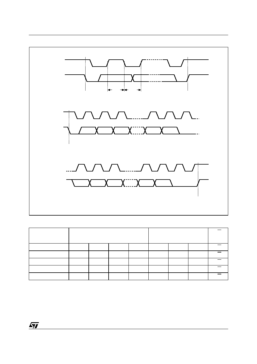
Figure 6. I≤C Bus Protocol
Table 3. Device Select Code
Note: 1. The most significant bit, b7, is sent first.
2. E0, E1 and E2 are compared against the respective external pins on the memory device.
3. A10, A9 and A8 represent most significant bits of the address.
Device Type Identifier
1
Chip Enable
2,3
RW
b7
b6
b5
b4
b3
b2
b1
b0
M24C01 Select Code
1
0
1
0
E2
E1
E0
RW
M24C02 Select Code
1
0
1
0
E2
E1
E0
RW
M24C04 Select Code
1
0
1
0
E2
E1
A8
RW
M24C08 Select Code
1
0
1
0
E2
A9
A8
RW
M24C16 Select Code
1
0
1
0
A10
A9
A8
RW
SCL
SDA
SCL
SDA
SDA
START
Condition
SDA
Input
SDA
Change
AI00792B
STOP
Condition
1
2
3
7
8
9
MSB
ACK
START
Condition
SCL
1
2
3
7
8
9
MSB
ACK
STOP
Condition