1/7
DATA BRIEF
October 2004
For further information contact your local ST sales office.
M25PXX
512 Kbit to 32 Mbit, Low Voltage, Serial Flash Memory
With 40 MHz or 50 MHz SPI Bus Interface
FEATURES SUMMARY
512Kbit to 32Mbit of Flash Memory
Page Program (up to 256 Bytes) in 1.4ms
(typical)
Sector Erase (256 Kbit or 512Kbit)
Bulk Erase (512Kbit to 32Mbit)
2.7 to 3.6V Single Supply Voltage
SPI Bus Compatible Serial Interface
40MHz to 50MHz Clock Rate (maximum)
Deep Power-down Mode 1
µ
A (typical)
Electronic Signatures
≠
JEDEC Standard Two-Byte Signature
(20xxh)
≠
RES Instruction, One-Byte, Signature, for
backward compatibility
More than 100000 Erase/Program Cycles per
Sector
More than 20 Year Data Retention
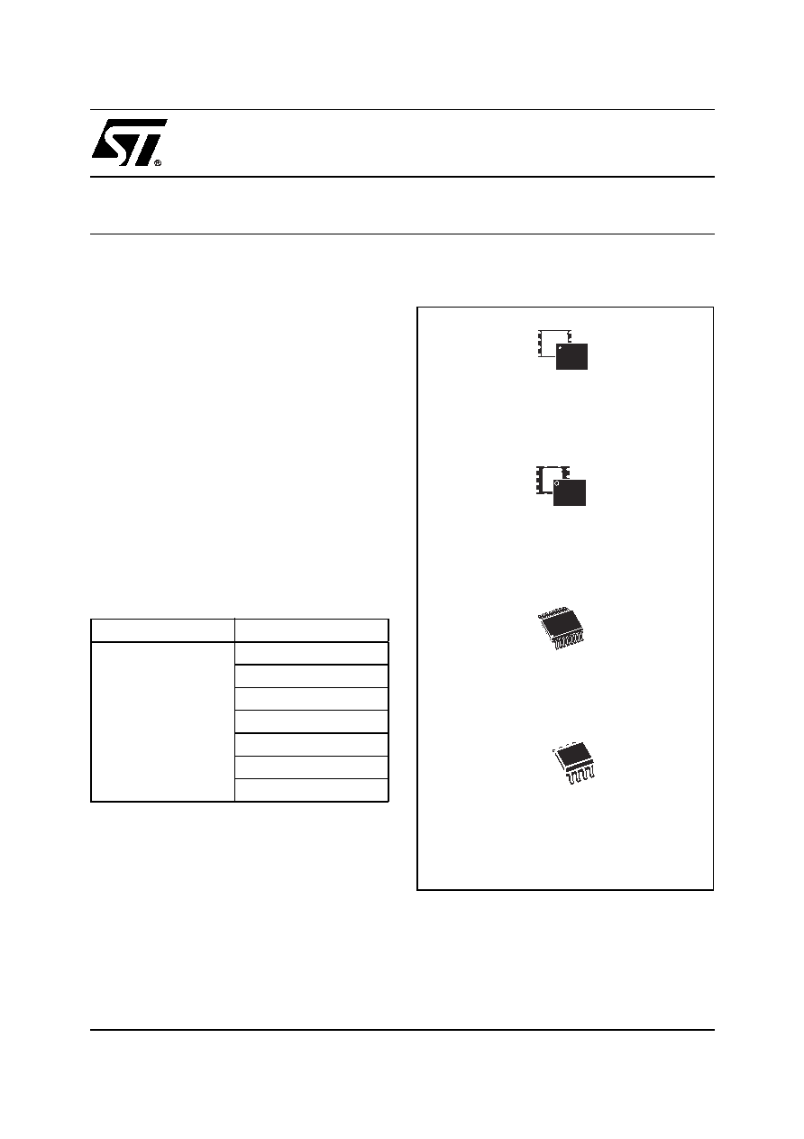
Table 1. Product List
Figure 1. Packages
Reference
Part Number
M25Pxx
M25P32
M25P16
M25P80
M25P40
M25P20
M25P10-A
M25P05-A
VDFPN8 (ME)
8x6mm (MLP8)
SO16 (MF)
300 mil width
SO8 (MN)
150 mil width
8
1
VDFPN8 (MP)
(MLP8)
M25PXX
2/7
SUMMARY DESCRIPTION
The M25Pxx is a 512Kbit to 32Mbit (2M x 8) Serial
Flash Memory, with advanced write protection
mechanisms, accessed by a high speed SPI-com-
patible bus.
The memory can be programmed 1 to 256 bytes at
a time, using the Page Program instruction.
The memory is organized as a number of sectors,
each containing 256 or 128 pages. Each page is
256 bytes wide.
The whole memory can be erased using the Bulk
Erase instruction, or a sector at a time, using the
Sector Erase instruction.
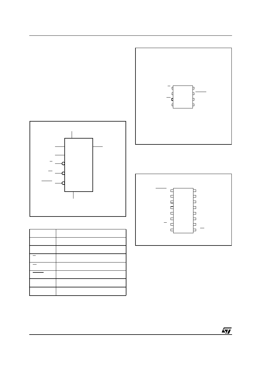
Figure 2. Logic Diagram
Table 2. Signal Names
Figure 3. SO8 and VDFPN Connections
Note: 1. There is an exposed die paddle on the underside of the
MLP8 package. This is pulled, internally, to V
SS
, and
must not be allowed to be connected to any other voltage
or signal line on the PCB.
Figure 4. SO16 Connections
Note: 1. DU = Don't Use
C Serial
Clock
D
Serial Data Input
Q
Serial Data Output
S
Chip Select
W Write
Protect
HOLD Hold
V
CC
Supply Voltage
V
SS
Ground
AI10258
S
VCC
M25Pxx
HOLD
VSS
W
Q
C
D
1
AI10259
2
3
4
8
7
6
5
D
VSS
C
HOLD
Q
S
VCC
W
M25Pxx
1
AI10260
2
3
4
16
15
14
13
DU
DU
DU
DU
VCC
HOLD
DU
DU
M25Pxx
5
6
7
8
12
11
10
9
W
Q
VSS
DU
DU
S
D
C
3/7
M25PXX
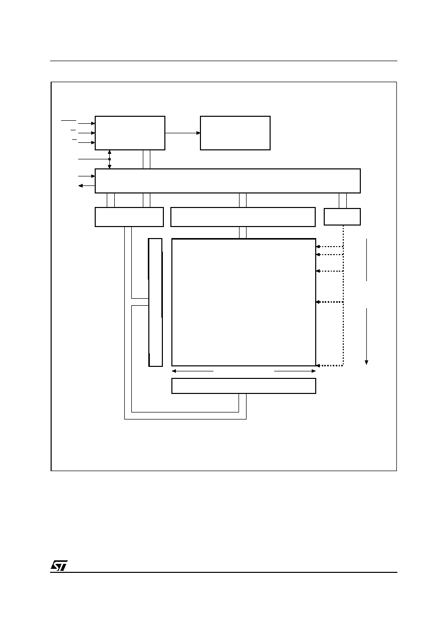
Figure 5. Block Diagram
AI10261
HOLD
S
W
Control Logic
High Voltage
Generator
I/O Shift Register
Address Register
and Counter
256 Byte
Data Buffer
256 Bytes (Page Size)
X Decoder
Y Decoder
Size of the
read-only
memory area
C
D
Q
Status
Register
00000h
Top of Address Space
000FFh
M25PXX
4/7
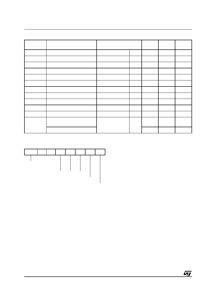
Table 3. Instruction Set
Table 4. Status Register Format
Instruction
Description
One-byte Instruction Code
Address
Bytes
Dummy
Bytes
Data
Bytes
WREN
Write Enable
0000 0110
06h
0
0
0
WRDI
Write Disable
0000 0100
04h
0
0
0
RDID
Read Identification
1001 1111
9Fh
0
0
1 to 3
RDSR
Read Status Register
0000 0101
05h
0
0
1 to
WRSR
Write Status Register
0000 0001
01h
0
0
1
READ
Read Data Bytes
0000 0011
03h
3
0
1 to
FAST_READ Read Data Bytes at Higher Speed
0000 1011
0Bh
3
1
1 to
PP
Page Program
0000 0010
02h
3
0
1 to 256
SE
Sector
Erase
1101
1000
D8h
3 0 0
BE
Bulk Erase
1100 0111
C7h
0
0
0
DP
Deep Power-down
1011 1001
B9h
0
0
0
RES
Release from Deep Power-down,
and Read Electronic Signature
1010 1011
ABh
0 3
1
to
Release from Deep Power-down
0
0
0
b7 b0
SRWD
0
0 BP2 BP1 BP0 WEL WIP
Status Register
Write Protect
Block Protect Bits
Write Enable Latch Bit
Write In Progress Bit
5/7
M25PXX
PART NUMBERING
Table 5. Ordering Information Scheme
Note: 1. ST strongly recommends the use of the Automotive Grade devices for use in an automotive environment. The High Reliability Cer-
tified Flow (HRCF) is described in the quality note QNEE9801. Please ask your nearest ST sales office for a copy.
For a list of available options (speed, package,
etc.) or for further information on any aspect of this
device, please contact your nearest ST Sales Of-
fice.
Example:
M25P80
≠
V
MP
6
T
P
Device Type
M25P = Serial Flash Memory for Code Storage
Device Function
32 = 32Mbit (4M x 8)
16 = 16Mbit (2M x 8)
80 = 8Mbit (1M x 8)
40 = 4Mbit (512K x 8)
20 = 2Mbit (256K x 8)
10-A = 1Mbit (128K x 8)
05-A = 512Kbit (64K x 8)
Operating Voltage
V = V
CC
= 2.7 to 3.6V
Package
ME = VDFPN8 8x6mm (MLP8)
MP = VDFPN8 (MLP8)
MF = SO16 (300 mil width)
MN = SO8 (150 mil width)
Device Grade
6 = Industrial temperature range, ≠40 to 85 ∞C.
Device tested with standard test flow
3 = Device tested with High Reliability Certified Flow
1
.
Automotive temperature range (≠40 to 125 ∞C)
Option
blank = Standard Packing
T = Tape and Reel Packing
Plating Technology
blank = Standard SnPb plating
P = Lead-Free and RoHS compliant
G = Lead-Free, RoHS compliant, Sb
2
O
3
-free and TBBA-free