
1/21
PRELIMINARY DATA
June 2000
This is preliminary information on a new product now in development or undergoing evaluation. Details are subject to change without notice.
M25P10
1 Mbit Low Voltage Paged Flash Memory
With 20 MHz Serial SPI Bus Interface
s
1 Mbit PAGED Flash Memory
s
128 BYTE PAGE PROGRAM IN 3 ms TYPICAL
s
256 Kbit SECTOR ERASE IN 1 s TYPICAL
s
BULK ERASE IN 2 s TYPICAL
s
SINGLE 2.7 V to 3.6 V SUPPLY VOLTAGE
s
SPI BUS COMPATIBLE SERIAL INTERFACE
s
20 MHz CLOCK RATE AVAILABLE
s
SUPPORTS POSITIVE CLOCK SPI MODES
s
DEEP POWER DOWN MODE (1 µA TYPICAL)
s
ELECTRONIC SIGNATURE
s
10,000 ERASE/PROG CYCLES PER SECTOR
s
20 YEARS DATA RETENTION
s
≠40 TO 85∞C TEMPERATURE RANGE
DESCRIPTION
The M25P10 is an 1 Mbit Paged Flash Memory
fabricated with STMicroelectronics High
Endurance CMOS technology. The memory is
accessed by a simple SPI bus compatible serial
interface. The bus signals are a serial clock input
(C), a serial data input (D) and a serial data output
(Q).
The device connected to the bus is selected when
the chip select input (S) goes low. Data is clocked
in during the low to high transition of clock C, data
Figure 1. Logic Diagram
AI03744
S
VCC
M25P10
HOLD
VSS
W
Q
C
D
Table 1. Signal Names
C Serial
Clock
D
Serial Data Input
Q
Serial Data Output
S
Chip Select
W Write
Protect
HOLD Hold
V
CC
Supply Voltage
V
SS
Ground
SO8 (MN)
150 mil width
8
1
SO8 (MW)
200 mil width
8
1
M25P10
2/21
is clocked out during the high to low transition of
clock C
SIGNALS DESCRIPTION
Serial Output (Q)
The output pin is used to transfer data serially out
of the memory. Data is shifted out on the falling
edge of the serial clock.
Serial Input (D)
The input pin is used to transfer data serially into
the device. It receives instructions, addresses,
and the data to be programmed. Input is latched
on the rising edge of the serial clock.
Serial Clock (C)
The serial clock provides the timing of the serial
interface. Instructions, addresses, or data present
at the input pin are latched on the rising edge of
the clock input, while data on the Q pin changes
after the falling edge of the clock input.
Chip Select (S)
When S is high, the memory is deselected and the
Q output pin is at high impedance and, unless an
internal Read, Program, Erase or Write Status
Register operation is underway, the device will be
in the Standby Power mode (this is not the Deep
Power Down mode). S low enables the memory,
placing it in the active power mode. It should be
noted that after power-on, a high to low transition
on S is required prior to the start of any operation.
Hold (HOLD)
The HOLD pin is used to pause serial
communications with a SPI memory without
resetting the serial sequence. To take the Hold
condition into account, the product must be
selected. The HOLD condition is validated by a 0
state on the Hold pin synchronized with the 0 state
on the Clock, as shown in Figure 4. The DeHOLD
condition is validated by a 1 state on the Hold pin
synchronized with the 0 state on the Clock. During
the Hold condition D, Q, and C are at a high
impedance state.
When the memory is under HOLD condition, it is
possible to deselect the device. Then, the protocol
is reset. The memory remains on HOLD as long as
the Hold pin is Low. To restart communication with
the device, it is necessary to both DeHOLD (H =
1) and to SELECT the memory.
Write Protect (W)
This pin is for hardware write protection of the
Status Register (SR); except WIP and WEL bits.
When bit 7 (SRWD) of the status register is 0 (the
initial delivery state); it is possible to write the SR
once the WEL (Write Enable Latch) has been set
with the WREN instruction and whatever is the
status of pin W (high or low).
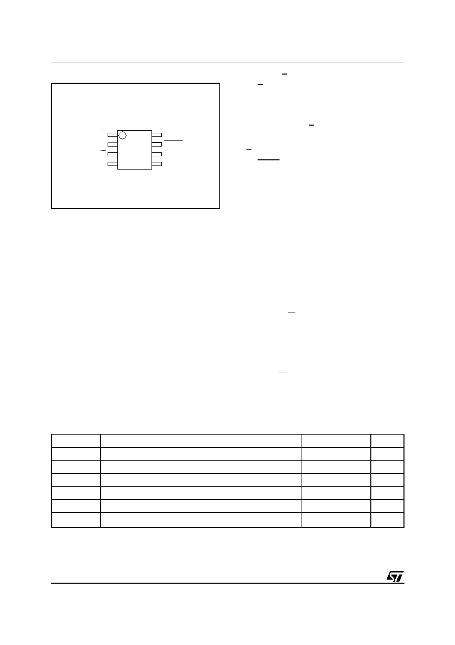
Figure 2. SO Connections
1
AI03745
2
3
4
8
7
6
5
D
VSS
C
HOLD
Q
S
VCC
W
M25P10
Table 2. Absolute Maximum Ratings
1
Note: 1. Except for the rating "Ambient Operating Temperature Range", stresses above those listed in this table may cause permanent
damage to the device. These are stress ratings only, and operation of the device at these or any other conditions above those
indicated in the Operating sections of this specification is not implied. Exposure to Absolute Maximum Rating conditions for
extended periods may affect device reliability. Refer also to the ST SURE Program and other relevant quality documents.
2. MIL-STD-883C, 3015.7 (100 pF, 1500
)
Symbol
Parameter
Value
Unit
T
A
Ambient Operating Temperature
≠40 to 85
∞C
T
STG
Storage Temperature
≠65 to 150
∞C
T
LEAD
Lead Temperature during Soldering
SO8: 40 seconds
215
∞C
V
IO
Input and Output Voltage Range (with respect to Ground)
≠0.3 to 5.0
V
V
CC
Supply Voltage Range
≠0.6 to 5.0
V
V
ESD
Electrostatic Discharge Voltage (Human Body model)
2
2000
V

3/21
M25P10
Once bit 7 (SRWD) of the status register has been
set to 1, the possibility to rewrite the SR depends
on the logical level present at pin W:
≠ If W pin is high, it will be possible to rewrite the
status register after having set the WEL (Write
Enable Latch).
≠ If W pin is low, any attempt to modify the status
register will be ignored by the device even if the
WEL was set. As a consequence: all the data
bytes in the memory area software protected
(SPM) by the BPi bits of the status register are
also hardware protected against data
modification and can be seen as a Read Only
memory area. This mode is called the Hardware
Protected Mode (HPM).
It is possible to enter the Hardware Protected
Mode (HPM) by setting SRWD bit after pulling
down the W pin or by pulling down the W pin after
setting SRWD bit.
The only way to abort the Hardware Protected
Mode once entered is to pull high the W pin.
If W pin is permanently tied to high level, the
Hardware Protected Mode will never be activated
and the memory will only allow the user to
software protect a part of the memory with the BPi
bits of the status register.
All protection features of the device are
summarized in Table 3.
Figure 3. Microcontroller and Memory Devices on the SPI Bus
AI03746
Master
(ST6, ST7, ST9,
ST10, Others)
M25P10
SDO
SDI
SCK
C
Q
D
S
M25P10
C
Q
D
S
M25P10
C
Q
D
S
CS3
CS2
CS1
SPI Interface with
(CPOL, CPHA) =
('0', '0') or ('1', '1')
Figure 4. Hold Condition Activation
AI02029B
HOLD PIN
CLOCK
ACTIVE
MEMORY
STATUS
HOLD
ACTIVE
HOLD
ACTIVE

M25P10
4/21
Clock Polarity (CPOL) and Clock Phase
(CPHA) with SPI Bus
As shown in Figure 5, the M25P10 can be driven
by a microcontroller with its SPI peripheral running
in either of the two following modes: (CPOL,
CPHA) = ('0', '0') or (CPOL, CPHA) = ('1', '1'). For
these two modes, input data is latched in by the
low to high transition of clock C, and output data is
available from the high to low transition of Clock
(C).The difference between (CPOL, CPHA) = (0,
0) and (CPOL, CPHA) = (1, 1) is the clock polarity
when in stand-by: C remains at '0' for (CPOL,
CPHA) = (0, 0) and C remains at '1' for (CPOL,
CPHA) = (1, 1) when there is no data transfer.
MEMORY ORGANIZATION
The memory is organized in 131,072 words of 8
bits each. The device features 1,024 pages of 128
bytes each. Each page can be individually
programmed (bits are programmed from `1' to '0'
state).
The device is also organized in 4 sectors of
262,144 bits (32,768 x 8 bits) each.The device is
Sector or Bulk Erasable but not Page Erasable
(bits are erased from '0' to '1' state).
OPERATIONS
All instructions, addresses and data are shifted in
and out of the chip MSB first. Data input (D) is
sampled on the first rising edge of clock (C) after
the chip select (S) goes low. Prior to any
Table 3. Protection Features
Note: 1. SPM: Software Protected Mode.
2. HPM: Hardware Protected Mode.
3. BPi: Bits BP0 and BP1 of the Status Register.
4. WEL: Write Enable Latch of the Status Register.
5. W: Write Protect Input Pin.
6. SRWD: Status Register Write Disable Bits of the Status Register.
7. The device is Bulk Erasable if, and only if, (BP0, BP1) = (0, 0), (see Bulk Erase paragraph).
W
SRWD
Status Register (SR)
Data Bytes (Software
Protected Area by BPi bits)
Mode
Data Bytes (Unprotected
Area)
X
0
Writeable after setting WEL
Software protected by the BPi
bits of the Status Register
SPM
Paged Programmable and
Sector Erasable
1
1
Writeable after setting WEL
Software protected by the BPi
bits of the Status Register
SPM
Paged Programmable and
Sector Erasable
0
1
Hardware protected
Hardware protected by the
BPi bits of the Status Register
and the W pin
HPM
Paged Programmable and
Sector Erasable
Table 4. Memory Organization
Sector Address
Range
3 18000h
1FFFFh
2 10000h
17FFFh
1 08000h
0FFFFh
0 00000h
07FFFh
Figure 5. M25P10-Compatible SPI Modes
AI01438
C
C
MSB
LSB
CPHA
D or Q
0
1
CPOL
0
1

5/21
M25P10
Figure 6. Block Diagram
AI03747
HOLD
S
W
Control Logic
High Voltage
Generator
I/O Shift Register
Address Register
and Counter
Data
Register
128 Bytes
X Decoder
Y Decoder
Size of the
Read only
Memory
area
C
D
Q
Status
1FFFFh
1FF80h
007Fh
0000h
An + 7Fh
An
Table 5. Protected Area Sizes
BP1
BP0
Software Protected Area
0 0
none
0
1
Upper quarter = Sector 3
1
0
Upper half = Sectors 2 & 3
1
1
Whole memory= Sectors 0, 1, 2 & 3