
1/34
December 2002
M25P05-A
512 Kbit, Low Voltage, Serial Flash Memory
With 25 MHz SPI Bus Interface
FEATURES SUMMARY
s
512 Kbit of Flash Memory
s
Page Program (up to 256 Bytes) in 1.5ms
(typical)
s
Sector Erase (256 Kbit) in 2 s (typical)
s
Bulk Erase (512 Kbit) in 3 s (typical)
s
2.7 V to 3.6 V Single Supply Voltage
s
SPI Bus Compatible Serial Interface
s
25 MHz Clock Rate (maximum)
s
Deep Power-down Mode 1
µ
A (typical)
s
Electronic Signature (05h)
s
More than 100,000 Erase/Program Cycles per
Sector
s
More than 20 Year Data Retention
Figure 1. Packages
ENHANCED VERSION OF THE M25P05
This device is an enhanced version of the
M25P05. The enhanced features include: larger
page size, shorter programming time, higher clock
frequency, specific electronic signature.
SO8 (MN)
150 mil width
8
1
VFQFPN8 (MP)
(MLP8)

M25P05-A
2/34
SUMMARY DESCRIPTION
The M25P05-A is a 512 Kbit (64K x 8) Serial Flash
Memory, with advanced write protection mecha-
nisms, accessed by a high speed SPI-compatible
bus.
The memory can be programmed 1 to 256 bytes at
a time, using the Page Program instruction.
The memory is organized as 2 sectors, each con-
taining 128 pages. Each page is 256 bytes wide.
Thus, the whole memory can be viewed as con-
sisting of 256 pages, or 65,536 bytes.
The whole memory can be erased using the Bulk
Erase instruction, or a sector at a time, using the
Sector Erase instruction.
Figure 2. Logic Diagram
Figure 3. SO Connections
Table 1. Signal Names
AI05757
S
VCC
M25P05-A
HOLD
VSS
W
Q
C
D
1
AI05758B
2
3
4
8
7
6
5
D
VSS
C
HOLD
Q
S
VCC
W
M25P05-A
C Serial
Clock
D
Serial Data Input
Q
Serial Data Output
S
Chip Select
W Write
Protect
HOLD Hold
V
CC
Supply Voltage
V
SS
Ground

3/34
M25P05-A
SIGNAL DESCRIPTION
Serial Data Output (Q). This output signal is
used to transfer data serially out of the device.
Data is shifted out on the falling edge of Serial
Clock (C).
Serial Data Input (D). This input signal is used to
transfer data serially into the device. It receives in-
structions, addresses, and the data to be pro-
grammed. Values are latched on the rising edge of
Serial Clock (C).
Serial Clock (C). This input signal provides the
timing of the serial interface. Instructions, address-
es, or data present at Serial Data Input (D) are
latched on the rising edge of Serial Clock (C). Data
on Serial Data Output (Q) changes after the falling
edge of Serial Clock (C).
Chip Select (S). When this input signal is High,
the device is deselected and Serial Data Output
(Q) is at high impedance. Unless an internal Pro-
gram, Erase or Write Status Register cycle is in
progress, the device will be in the Standby mode
(this is not the Deep Power-down mode). Driving
Chip Select (S) Low enables the device, placing it
in the active power mode.
After Power-up, a falling edge on Chip Select (S)
is required prior to the start of any instruction.
Hold (HOLD). The Hold (HOLD) signal is used to
pause any serial communications with the device
without deselecting the device.
During the Hold condition, the Serial Data Output
(Q) is high impedance, and Serial Data Input (D)
and Serial Clock (C) are Don't Care.
To start the Hold condition, the device must be se-
lected, with Chip Select (S) driven Low.
Write Protect (W). The main purpose of this in-
put signal is to freeze the size of the area of mem-
ory that is protected against program or erase
instructions (as specified by the values in the BP1
and BP0 bits of the Status Register).
M25P05-A
4/34
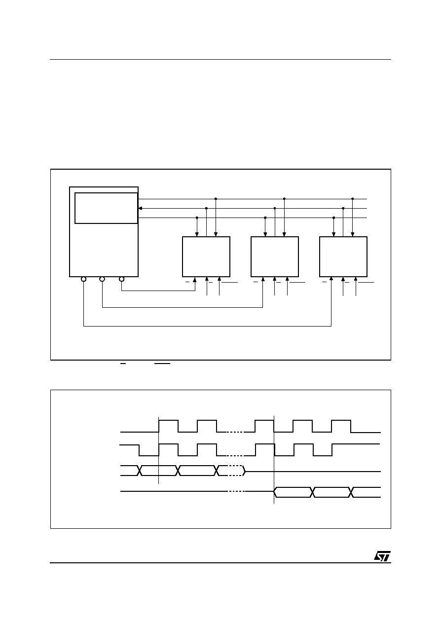
SPI MODES
These devices can be driven by a microcontroller
with its SPI peripheral running in either of the two
following modes:
≠ CPOL=0, CPHA=0
≠ CPOL=1, CPHA=1
For these two modes, input data is latched in on
the rising edge of Serial Clock (C), and output data
is available from the falling edge of Serial Clock
(C).
The difference between the two modes, as shown
in Figure 5, is the clock polarity when the bus mas-
ter is in Stand-by mode and not transferring data:
≠ C remains at 0 for (CPOL=0, CPHA=0)
≠ C remains at 1 for (CPOL=1, CPHA=1)
Figure 4. Bus Master and Memory Devices on the SPI Bus
Note: 1. The Write Protect (W) and Hold (HOLD) signals should be driven, High or Low as appropriate.
Figure 5. SPI Modes Supported
AI03746D
Bus Master
(ST6, ST7, ST9,
ST10, Others)
SPI Memory
Device
SDO
SDI
SCK
C
Q
D
S
SPI Memory
Device
C
Q
D
S
SPI Memory
Device
C
Q
D
S
CS3
CS2
CS1
SPI Interface with
(CPOL, CPHA) =
(0, 0) or (1, 1)
W
HOLD
W
HOLD
W
HOLD
AI01438B
C
MSB
CPHA
D
0
1
CPOL
0
1
Q
C
MSB

5/34
M25P05-A
OPERATING FEATURES
Page Programming
To program one data byte, two instructions are re-
quired: Write Enable (WREN), which is one byte,
and a Page Program (PP) sequence, which con-
sists of four bytes plus data. This is followed by the
internal Program cycle (of duration t
PP
).
To spread this overhead, the Page Program (PP)
instruction allows up to 256 bytes to be pro-
grammed at a time (changing bits from 1 to 0), pro-
vided that they lie in consecutive addresses on the
same page of memory.
Sector Erase and Bulk Erase
The Page Program (PP) instruction allows bits to
be reset from 1 to 0. Before this can be applied, the
bytes of memory need to have been erased to all
1s (FFh). This can be achieved either a sector at a
time, using the Sector Erase (SE) instruction, or
throughout the entire memory, using the Bulk
Erase (BE) instruction. This starts an internal
Erase cycle (of duration t
SE
or t
BE
).
The Erase instruction must be preceeded by a
Write Enable (WREN) instruction.
Polling During a Write, Program or Erase Cycle
A further improvement in the time to Write Status
Register (WRSR), Program (PP) or Erase (SE or
BE) can be achieved by not waiting for the worst
case delay (t
W
, t
PP
, t
SE
, or t
BE
). The Write In
Progress (WIP) bit is provided in the Status Regis-
ter so that the application program can monitor its
value, polling it to establish when the previous
Write cycle, Program cycle or Erase cycle is com-
plete.
Active Power, Stand-by Power and Deep
Power-Down Modes
When Chip Select (S) is Low, the device is en-
abled, and in the Active Power mode.
When Chip Select (S) is High, the device is dis-
abled, but could remain in the Active Power mode
until all internal cycles have completed (Program,
Erase, Write Status Register). The device then
goes in to the Stand-by Power mode. The device
consumption drops to I
CC1
.
The Deep Power-down mode is entered when the
specific instruction (the Enter Deep Power-down
Mode (DP) instruction) is executed. The device
consumption drops further to I
CC2
. The device re-
mains in this mode until another specific instruc-
tion (the Release from Deep Power-down Mode
and Read Electronic Signature (RES) instruction)
is executed.
All other instructions are ignored while the device
is in the Deep Power-down mode. This can be
used as an extra software protection mechanism,
when the device is not in active use, to protect the
device from inadvertant Write, Program or Erase
instructions.
Status Register
The Status Register contains a number of status
and control bits, as shown in Table 5, that can be
read or set (as appropriate) by specific instruc-
tions.
WIP bit. The Write In Progress (WIP) bit indicates
whether the memory is busy with a Write Status
Register, Program or Erase cycle.
WEL bit. The Write Enable Latch (WEL) bit indi-
cates the status of the internal Write Enable Latch.
BP1, BP0 bits. The Block Protect (BP1, BP0) bits
are non-volatile. They define the size of the area to
be software protected against Program and Erase
instructions.
SRWD bit. The Status Register Write Disable
(SRWD) bit is operated in conjunction with the
Write Protect (W) signal. The Status Register
Write Disable (SRWD) bit and Write Protect (W)
signal allow the device to be put in the Hardware
Protected mode. In this mode, the non-volatile bits
of the Status Register (SRWD, BP1, BP0) become
read-only bits.