Document Outline
- FEATURES SUMMARY
- SIGNAL DESCRIPTION
- SPI MODES
- OPERATING FEATURES
- MEMORY ORGANIZATION
- INSTRUCTIONS
- POWER-UP AND POWER-DOWN
- INITIAL DELIVERY STATE
- MAXIMUM RATING
- DC AND AC PARAMETERS
- PACKAGE MECHANICAL
- Figure 26. MLP8, 8-lead Very thin Dual Flat Package No lead, 6x5mm, Package Outline
- Table 16. MLP8, 8-lead Very thin Dual Flat Package No lead, 6x5mm, Package Mechanical Data
- Figure 27. SO8 Narrow - 8 lead Plastic Small Outline, 150 mils body width, Package Outline
- Table 17. SO8 Narrow - 8 lead Plastic Small Outline, 150 mils body width, Mechanical Data
- PART NUMBERING
- REVISION HISTORY
1/37
October 2005
M25PE20
M25PE10
1 and 2 Mbit, Low Voltage, Page-Erasable Serial Flash Memories
with Byte-Alterability, 33 MHz SPI Bus, Standard Pin-out
FEATURES SUMMARY
Industrial Standard SPI Pin-out
1 or 2 Mbit of Page-Erasable Flash Memory
Page Write (up to 256 Bytes) in 11ms (typical)
Page Program (up to 256 Bytes) in 1.2ms
(typical)
Page Erase (256 Bytes) in 10ms (typical)
Sector Erase (512 Kbit)
2.7 to 3.6V Single Supply Voltage
SPI Bus Compatible Serial Interface
33MHz Clock Rate (maximum)
Deep Power-down Mode 1
�
A (typical)
Electronic Signature
�
JEDEC Standard Two-Byte Signature
(8012h for M25PE20
8011h for M25PE10)
More than 100,000 Write Cycles
More than 20 Year Data Retention
Hardware Write Protection of the Top Sector
(64KB)
Packages
�
ECOPACK� (RoHS compliant)
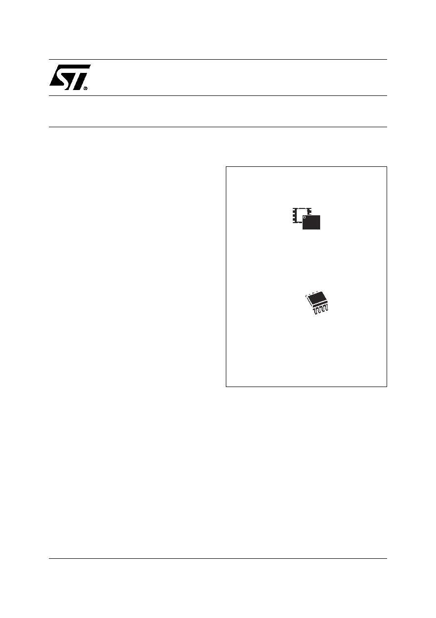
Figure 1. Packages
VDFPN8 (MP)
6x5mm (MLP8)
8
1
SO8N (MN)
150 mil width

M25PE10, M25PE20
2/37
TABLE OF CONTENTS
FEATURES SUMMARY . . . . . . . . . . . . . . . . . . . . . . . . . . . . . . . . . . . . . . . . . . . . . . . . . . . . . . . . . . . . . 1
SIGNAL DESCRIPTION . . . . . . . . . . . . . . . . . . . . . . . . . . . . . . . . . . . . . . . . . . . . . . . . . . . . . . . . . . . . . 5
Serial Data Output (Q) . . . . . . . . . . . . . . . . . . . . . . . . . . . . . . . . . . . . . . . . . . . . . . . . . . . . . . . . . . . . 5
Serial Data Input (D) . . . . . . . . . . . . . . . . . . . . . . . . . . . . . . . . . . . . . . . . . . . . . . . . . . . . . . . . . . . . . 5
Serial Clock (C) . . . . . . . . . . . . . . . . . . . . . . . . . . . . . . . . . . . . . . . . . . . . . . . . . . . . . . . . . . . . . . . . . 5
Chip Select (S) . . . . . . . . . . . . . . . . . . . . . . . . . . . . . . . . . . . . . . . . . . . . . . . . . . . . . . . . . . . . . . . . . 5
Reset (Reset) . . . . . . . . . . . . . . . . . . . . . . . . . . . . . . . . . . . . . . . . . . . . . . . . . . . . . . . . . . . . . . . . . . 5
Top Sector Lock (TSL) . . . . . . . . . . . . . . . . . . . . . . . . . . . . . . . . . . . . . . . . . . . . . . . . . . . . . . . . . . . 5
SPI MODES . . . . . . . . . . . . . . . . . . . . . . . . . . . . . . . . . . . . . . . . . . . . . . . . . . . . . . . . . . . . . . . . . . . . . . . 6
OPERATING FEATURES . . . . . . . . . . . . . . . . . . . . . . . . . . . . . . . . . . . . . . . . . . . . . . . . . . . . . . . . . . . . 7
Sharing the Overhead of Modifying Data . . . . . . . . . . . . . . . . . . . . . . . . . . . . . . . . . . . . . . . . . . . 7
An Easy Way to Modify Data . . . . . . . . . . . . . . . . . . . . . . . . . . . . . . . . . . . . . . . . . . . . . . . . . . . . . 7
A Fast Way to Modify Data . . . . . . . . . . . . . . . . . . . . . . . . . . . . . . . . . . . . . . . . . . . . . . . . . . . . . . . 7
Polling During a Write, Program or Erase Cycle . . . . . . . . . . . . . . . . . . . . . . . . . . . . . . . . . . . . . 7
Reset . . . . . . . . . . . . . . . . . . . . . . . . . . . . . . . . . . . . . . . . . . . . . . . . . . . . . . . . . . . . . . . . . . . . . . . . . 7
Active Power, Standby Power and Deep Power-Down Modes . . . . . . . . . . . . . . . . . . . . . . . . . . 7
Status Register . . . . . . . . . . . . . . . . . . . . . . . . . . . . . . . . . . . . . . . . . . . . . . . . . . . . . . . . . . . . . . . . 8
WIP bit . . . . . . . . . . . . . . . . . . . . . . . . . . . . . . . . . . . . . . . . . . . . . . . . . . . . . . . . . . . . . . . . . . . . . . . . 8
WEL bit . . . . . . . . . . . . . . . . . . . . . . . . . . . . . . . . . . . . . . . . . . . . . . . . . . . . . . . . . . . . . . . . . . . . . . . 8
Protection Modes . . . . . . . . . . . . . . . . . . . . . . . . . . . . . . . . . . . . . . . . . . . . . . . . . . . . . . . . . . . . . . 8
MEMORY ORGANIZATION . . . . . . . . . . . . . . . . . . . . . . . . . . . . . . . . . . . . . . . . . . . . . . . . . . . . . . . . . . 9
INSTRUCTIONS . . . . . . . . . . . . . . . . . . . . . . . . . . . . . . . . . . . . . . . . . . . . . . . . . . . . . . . . . . . . . . . . . . 12
Write Enable (WREN) . . . . . . . . . . . . . . . . . . . . . . . . . . . . . . . . . . . . . . . . . . . . . . . . . . . . . . . . . . 13
Write Disable (WRDI) . . . . . . . . . . . . . . . . . . . . . . . . . . . . . . . . . . . . . . . . . . . . . . . . . . . . . . . . . . . 13
Read Identification (RDID) . . . . . . . . . . . . . . . . . . . . . . . . . . . . . . . . . . . . . . . . . . . . . . . . . . . . . . 14
Read Status Register (RDSR) . . . . . . . . . . . . . . . . . . . . . . . . . . . . . . . . . . . . . . . . . . . . . . . . . . . . 15
WIP bit . . . . . . . . . . . . . . . . . . . . . . . . . . . . . . . . . . . . . . . . . . . . . . . . . . . . . . . . . . . . . . . . . . . . . . . 15
WEL bit . . . . . . . . . . . . . . . . . . . . . . . . . . . . . . . . . . . . . . . . . . . . . . . . . . . . . . . . . . . . . . . . . . . . . . 15
Read Data Bytes (READ). . . . . . . . . . . . . . . . . . . . . . . . . . . . . . . . . . . . . . . . . . . . . . . . . . . . . . . . 16
Read Data Bytes at Higher Speed (FAST_READ) . . . . . . . . . . . . . . . . . . . . . . . . . . . . . . . . . . . . 17
Page Write (PW) . . . . . . . . . . . . . . . . . . . . . . . . . . . . . . . . . . . . . . . . . . . . . . . . . . . . . . . . . . . . . . . 18
Page Program (PP) . . . . . . . . . . . . . . . . . . . . . . . . . . . . . . . . . . . . . . . . . . . . . . . . . . . . . . . . . . . . 19
Page Erase (PE) . . . . . . . . . . . . . . . . . . . . . . . . . . . . . . . . . . . . . . . . . . . . . . . . . . . . . . . . . . . . . . . 20
Sector Erase (SE) . . . . . . . . . . . . . . . . . . . . . . . . . . . . . . . . . . . . . . . . . . . . . . . . . . . . . . . . . . . . . 21
Deep Power-down (DP) . . . . . . . . . . . . . . . . . . . . . . . . . . . . . . . . . . . . . . . . . . . . . . . . . . . . . . . . . 22
Release from Deep Power-down (RDP) . . . . . . . . . . . . . . . . . . . . . . . . . . . . . . . . . . . . . . . . . . . . 23
POWER-UP AND POWER-DOWN . . . . . . . . . . . . . . . . . . . . . . . . . . . . . . . . . . . . . . . . . . . . . . . . . . . . 24

3/37
M25PE10, M25PE20
INITIAL DELIVERY STATE. . . . . . . . . . . . . . . . . . . . . . . . . . . . . . . . . . . . . . . . . . . . . . . . . . . . . . . . . . 25
MAXIMUM RATING. . . . . . . . . . . . . . . . . . . . . . . . . . . . . . . . . . . . . . . . . . . . . . . . . . . . . . . . . . . . . . . . 25
DC and AC PARAMETERS . . . . . . . . . . . . . . . . . . . . . . . . . . . . . . . . . . . . . . . . . . . . . . . . . . . . . . . . . 26
PACKAGE MECHANICAL . . . . . . . . . . . . . . . . . . . . . . . . . . . . . . . . . . . . . . . . . . . . . . . . . . . . . . . . . . 33
PART NUMBERING . . . . . . . . . . . . . . . . . . . . . . . . . . . . . . . . . . . . . . . . . . . . . . . . . . . . . . . . . . . . . . . 35
REVISION HISTORY. . . . . . . . . . . . . . . . . . . . . . . . . . . . . . . . . . . . . . . . . . . . . . . . . . . . . . . . . . . . . . . 36

M25PE10, M25PE20
4/37
SUMMARY DESCRIPTION
The M25PE20 and M25PE10 are 2 Mbit (256K x 8
bit) and 1 Mbit (128K x8 bit) Serial Paged Flash
Memories, respectively. They are accessed by a
high speed SPI-compatible bus.
The memories can be written or programmed 1 to
256 Bytes at a time, using the Page Write or Page
Program instruction. The Page Write instruction
consists of an integrated Page Erase cycle fol-
lowed by a Page Program cycle.
The M25PE20 memory is organized as 4 sectors,
each containing 256 pages. Each page is 256
Bytes wide. Thus, the whole memory can be
viewed as consisting of 1024 pages, or 262,144
Bytes.
The M25PE10 memory is organized as 2 sectors,
each containing 256 pages. Each page is 256
Bytes wide. Thus, the whole memory can be
viewed as consisting of 512 pages, or 131, 072
Bytes.
The memories can be erased a page at a time, us-
ing the Page Erase instruction, or a sector at a
time, using the Sector Erase instruction.
The top sector of the memories can be Write Pro-
tected by Hardware (TSL).
In order to meet environmental requirements, ST
offers these devices in ECOPACK� packages.
ECOPACK� packages are Lead-free and RoHS
compliant.
ECOPACK is an ST trademark. ECOPACK speci-
fications are available at: www.st.com.
Figure 2. Logic Diagram
Table 1. Signal Names
Figure 3. VDFPN AND SO Connections
Note: 1. There is an exposed die paddle on the underside of the
MLP8 package. This is pulled, internally, to V
SS
, and
must not be allowed to be connected to any other voltage
or signal line on the PCB.
2. See
PACKAGE MECHANICAL
section for package di-
mensions, and how to identify pin-1.
Reset
AI09713
S
VCC
M25PE20
M25PE10
VSS
TSL
Q
C
D
C Serial
Clock
D
Serial Data Input
Q
Serial Data Output
S
Chip Select
TSL
Top Sector Lock
Reset Reset
V
CC
Supply Voltage
V
SS
Ground
1
AI09715
2
3
4
8
7
6
5
D
VSS
C
Reset
Q
S
VCC
TSL
M25PE20
M25PE10

5/37
M25PE10, M25PE20
SIGNAL DESCRIPTION
Serial Data Output (Q). This output signal is
used to transfer data serially out of the device.
Data is shifted out on the falling edge of Serial
Clock (C).
Serial Data Input (D). This input signal is used to
transfer data serially into the device. It receives in-
structions, addresses, and the data to be pro-
grammed. Values are latched on the rising edge of
Serial Clock (C).
Serial Clock (C). This input signal provides the
timing of the serial interface. Instructions, address-
es, or data present at Serial Data Input (D) are
latched on the rising edge of Serial Clock (C). Data
on Serial Data Output (Q) changes after the falling
edge of Serial Clock (C).
Chip Select (S). When this input signal is High,
the device is deselected and Serial Data Output
(Q) is at high impedance. Unless an internal Read,
Program, Erase or Write cycle is in progress, the
device will be in the Standby Power mode (this is
not the Deep Power-down mode). Driving Chip
Select (S) Low selects the device, placing it in the
Active Power mode.
After Power-up, a falling edge on Chip Select (S)
is required prior to the start of any instruction.
Reset (Reset). The Reset (Reset) input provides
a hardware reset for the memory.
When Reset (Reset) is driven High, the memory is
in the normal operating mode. When Reset (Re-
set) is driven Low, the memory will enter the Reset
mode. In this mode, the output is high impedance.
Driving Reset (Reset) Low while an internal oper-
ation is in progress will affect this operation (write,
program or erase cycle) and data may be lost.
Top Sector Lock (TSL). This input signal puts
the device in the Hardware Protected mode, when
Top Sector Lock (TSL) is connected to V
SS
, caus-
ing the top 256 pages (upper addresses) of the
memory to become read-only (protected from
write, program and erase operations).
When Top Sector Lock (TSL) is connected to V
CC
,
the top 256 pages of memory behave like the other
pages of memory.