Document Outline
- FEATURES SUMMARY
- SIGNAL DESCRIPTION
- SPI MODES
- OPERATING FEATURES
- MEMORY ORGANIZATION
- INSTRUCTIONS
- POWER-UP AND POWER-DOWN
- INITIAL DELIVERY STATE
- MAXIMUM RATING
- DC and AC PARAMETERS
- PACKAGE MECHANICAL
- Figure 29. MLP8, 8-lead Very thin Dual Flat Package No lead, 6x5mm, Package Outline
- Table 18. MLP8, 8-lead Very thin Dual Flat Package No lead, 6x5mm, Package Mechanical Data
- Figure 30. SO8 wide � 8 lead Plastic Small Outline, 208 mils body width, Package Outline
- Table 19. SO8 wide � 8 lead Plastic Small Outline, 208 mils body width, Mechanical Data
- PART NUMBERING
- REVISION HISTORY
1/43
PRELIMINARY DATA
August 2005
This is preliminary information on a new product now in development or undergoing evaluation. Details are subject to change without notice.
M25PE80
8 Mbit, Low Voltage, Page-Erasable Serial Flash Memory with
Byte-Alterability, 50MHz SPI Bus, Standard Pin-out
FEATURES SUMMARY
Industrial Standard SPI Pin-out
8 Mbits of Page-Erasable Flash Memory
Page Write (up to 256 Bytes) in 11ms (typical)
Page Program (up to 256 Bytes) in 1.2ms
(typical)
Page Erase (256 Bytes) in 10ms (typical)
Sector Erase (512 Kbits)
Bulk Erase (8 Mbits)
2.7 to 3.6V Single Supply Voltage
SPI Bus Compatible Serial Interface
50MHz Clock Rate (maximum)
Deep Power-down Mode 1
�
A (typical)
Electronic Signature
�
JEDEC Standard Two-Byte Signature
(8014h)
More than 100,000 Write Cycles
More than 20 Year Data Retention
Hardware Write Protection of the Top Sector
(64KB)
Software Write Protection on a 64KByte
Sector Basis
Software Write Protection on a 4KByte Sub-
sector Basis for Sector 0 and Sector 15
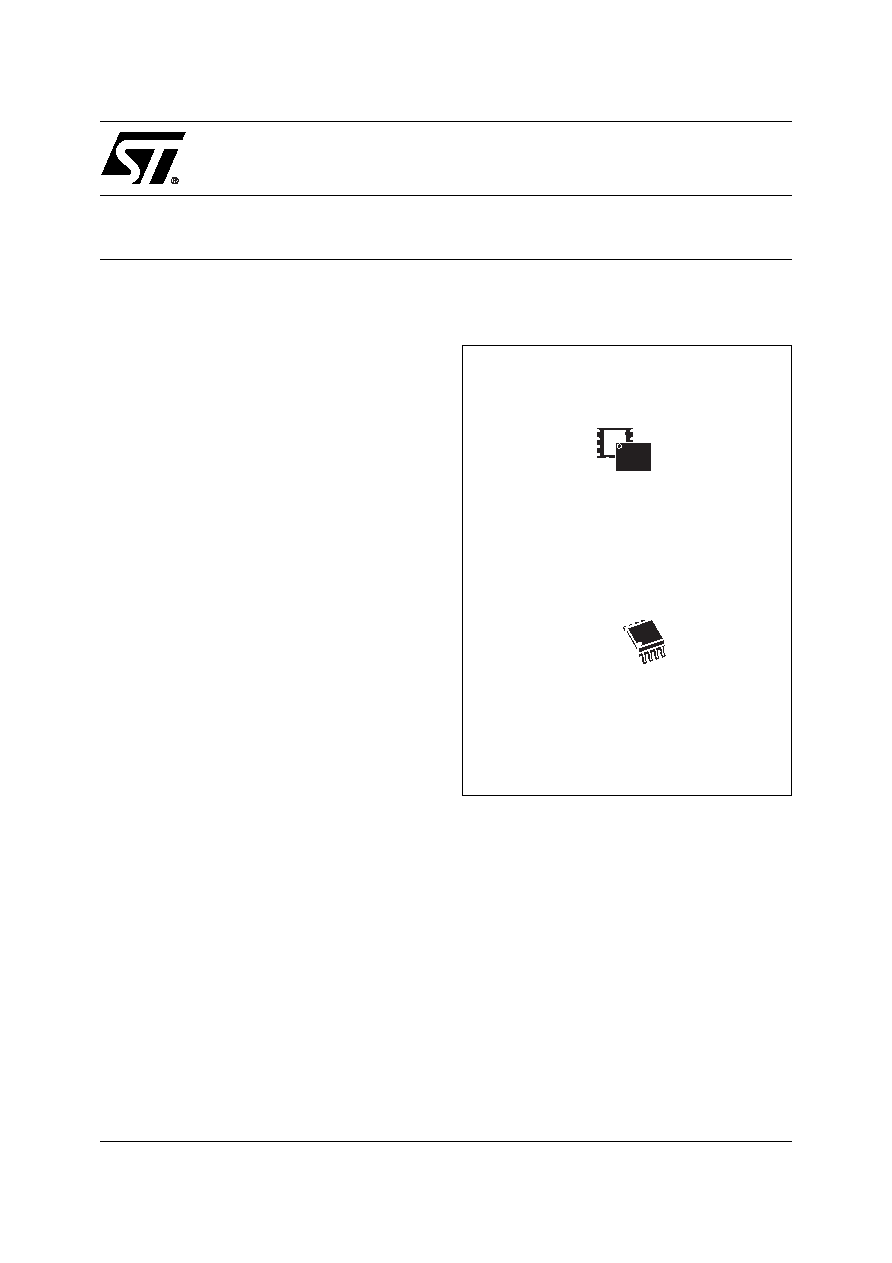
Figure 1. Packages
VDFPN8 (MP)
6 x 5mm (MLP8)
8
1
SO8W (MW)
208 mils width

M25PE80
2/43
TABLE OF CONTENTS
FEATURES SUMMARY . . . . . . . . . . . . . . . . . . . . . . . . . . . . . . . . . . . . . . . . . . . . . . . . . . . . . . . . . . . . . 1
Figure 1. Packages . . . . . . . . . . . . . . . . . . . . . . . . . . . . . . . . . . . . . . . . . . . . . . . . . . . . . . . . . . . . . . 1
Figure 2. Logic Diagram . . . . . . . . . . . . . . . . . . . . . . . . . . . . . . . . . . . . . . . . . . . . . . . . . . . . . . . . . . 5
Table 1. Signal Names . . . . . . . . . . . . . . . . . . . . . . . . . . . . . . . . . . . . . . . . . . . . . . . . . . . . . . . . . . 5
Figure 3. VDFPN and SO Connections . . . . . . . . . . . . . . . . . . . . . . . . . . . . . . . . . . . . . . . . . . . . . . 5
SIGNAL DESCRIPTION . . . . . . . . . . . . . . . . . . . . . . . . . . . . . . . . . . . . . . . . . . . . . . . . . . . . . . . . . . . . . 6
Serial Data Output (Q) . . . . . . . . . . . . . . . . . . . . . . . . . . . . . . . . . . . . . . . . . . . . . . . . . . . . . . . . . . . . 6
Serial Data Input (D) . . . . . . . . . . . . . . . . . . . . . . . . . . . . . . . . . . . . . . . . . . . . . . . . . . . . . . . . . . . . . 6
Serial Clock (C) . . . . . . . . . . . . . . . . . . . . . . . . . . . . . . . . . . . . . . . . . . . . . . . . . . . . . . . . . . . . . . . . . 6
Chip Select (S) . . . . . . . . . . . . . . . . . . . . . . . . . . . . . . . . . . . . . . . . . . . . . . . . . . . . . . . . . . . . . . . . . 6
Reset (Reset) . . . . . . . . . . . . . . . . . . . . . . . . . . . . . . . . . . . . . . . . . . . . . . . . . . . . . . . . . . . . . . . . . . 6
Top Sector Lock (TSL) . . . . . . . . . . . . . . . . . . . . . . . . . . . . . . . . . . . . . . . . . . . . . . . . . . . . . . . . . . . 6
SPI MODES . . . . . . . . . . . . . . . . . . . . . . . . . . . . . . . . . . . . . . . . . . . . . . . . . . . . . . . . . . . . . . . . . . . . . . . 7
Figure 4. Bus Master and Memory Devices on the SPI Bus. . . . . . . . . . . . . . . . . . . . . . . . . . . . . . . 7
Figure 5. SPI Modes Supported . . . . . . . . . . . . . . . . . . . . . . . . . . . . . . . . . . . . . . . . . . . . . . . . . . . . 7
OPERATING FEATURES . . . . . . . . . . . . . . . . . . . . . . . . . . . . . . . . . . . . . . . . . . . . . . . . . . . . . . . . . . . . 8
Sharing the Overhead of Modifying Data . . . . . . . . . . . . . . . . . . . . . . . . . . . . . . . . . . . . . . . . . . . 8
An Easy Way to Modify Data . . . . . . . . . . . . . . . . . . . . . . . . . . . . . . . . . . . . . . . . . . . . . . . . . . . . . 8
A Fast Way to Modify Data . . . . . . . . . . . . . . . . . . . . . . . . . . . . . . . . . . . . . . . . . . . . . . . . . . . . . . . 8
Polling During a Write, Program or Erase Cycle . . . . . . . . . . . . . . . . . . . . . . . . . . . . . . . . . . . . . 8
Reset . . . . . . . . . . . . . . . . . . . . . . . . . . . . . . . . . . . . . . . . . . . . . . . . . . . . . . . . . . . . . . . . . . . . . . . . . 8
Active Power, Standby Power and Deep Power-Down Modes . . . . . . . . . . . . . . . . . . . . . . . . . . 8
Status Register . . . . . . . . . . . . . . . . . . . . . . . . . . . . . . . . . . . . . . . . . . . . . . . . . . . . . . . . . . . . . . . . 9
WIP bit . . . . . . . . . . . . . . . . . . . . . . . . . . . . . . . . . . . . . . . . . . . . . . . . . . . . . . . . . . . . . . . . . . . . . . . . 9
WEL bit . . . . . . . . . . . . . . . . . . . . . . . . . . . . . . . . . . . . . . . . . . . . . . . . . . . . . . . . . . . . . . . . . . . . . . . 9
Table 2. Status Register Format . . . . . . . . . . . . . . . . . . . . . . . . . . . . . . . . . . . . . . . . . . . . . . . . . . . 9
Protection Modes . . . . . . . . . . . . . . . . . . . . . . . . . . . . . . . . . . . . . . . . . . . . . . . . . . . . . . . . . . . . . . 9
Table 3. Software Protection Truth Table (Sectors 1 to 14) . . . . . . . . . . . . . . . . . . . . . . . . . . . . . 10
Table 4. Software Protection Scheme Truth Table (Sectors 0 and 15) . . . . . . . . . . . . . . . . . . . . . 10
Figure 6. Software Protection Scheme . . . . . . . . . . . . . . . . . . . . . . . . . . . . . . . . . . . . . . . . . . . . . . 11
MEMORY ORGANIZATION . . . . . . . . . . . . . . . . . . . . . . . . . . . . . . . . . . . . . . . . . . . . . . . . . . . . . . . . . 12
Table 5. Memory Organization . . . . . . . . . . . . . . . . . . . . . . . . . . . . . . . . . . . . . . . . . . . . . . . . . . . 12
Figure 7. Block Diagram . . . . . . . . . . . . . . . . . . . . . . . . . . . . . . . . . . . . . . . . . . . . . . . . . . . . . . . . . 13
INSTRUCTIONS . . . . . . . . . . . . . . . . . . . . . . . . . . . . . . . . . . . . . . . . . . . . . . . . . . . . . . . . . . . . . . . . . . 14
Table 6. Instruction Set . . . . . . . . . . . . . . . . . . . . . . . . . . . . . . . . . . . . . . . . . . . . . . . . . . . . . . . . . 14
Write Enable (WREN) . . . . . . . . . . . . . . . . . . . . . . . . . . . . . . . . . . . . . . . . . . . . . . . . . . . . . . . . . . 15
Figure 8. Write Enable (WREN) Instruction Sequence . . . . . . . . . . . . . . . . . . . . . . . . . . . . . . . . . . 15
Write Disable (WRDI) . . . . . . . . . . . . . . . . . . . . . . . . . . . . . . . . . . . . . . . . . . . . . . . . . . . . . . . . . . . 15

3/43
M25PE80
Figure 9. Write Disable (WRDI) Instruction Sequence . . . . . . . . . . . . . . . . . . . . . . . . . . . . . . . . . . 15
Read Identification (RDID) . . . . . . . . . . . . . . . . . . . . . . . . . . . . . . . . . . . . . . . . . . . . . . . . . . . . . . 16
Table 7. Read Identification (RDID) Data-Out Sequence . . . . . . . . . . . . . . . . . . . . . . . . . . . . . . . 16
Figure 10.Read Identification (RDID) Instruction Sequence and Data-Out Sequence . . . . . . . . . . 16
Read Status Register (RDSR) . . . . . . . . . . . . . . . . . . . . . . . . . . . . . . . . . . . . . . . . . . . . . . . . . . . . 17
WIP bit . . . . . . . . . . . . . . . . . . . . . . . . . . . . . . . . . . . . . . . . . . . . . . . . . . . . . . . . . . . . . . . . . . . . . . . 17
WEL bit . . . . . . . . . . . . . . . . . . . . . . . . . . . . . . . . . . . . . . . . . . . . . . . . . . . . . . . . . . . . . . . . . . . . . . 17
Figure 11.Read Status Register (RDSR) Instruction Sequence and Data-Out Sequence . . . . . . . 17
Read Data Bytes (READ). . . . . . . . . . . . . . . . . . . . . . . . . . . . . . . . . . . . . . . . . . . . . . . . . . . . . . . . 18
Figure 12.Read Data Bytes (READ) Instruction Sequence and Data-Out Sequence . . . . . . . . . . . 18
Read Data Bytes at Higher Speed (FAST_READ) . . . . . . . . . . . . . . . . . . . . . . . . . . . . . . . . . . . . 19
Figure 13.Read Data Bytes at Higher Speed (FAST_READ) Instruction Sequence
and Data-Out Sequence . . . . . . . . . . . . . . . . . . . . . . . . . . . . . . . . . . . . . . . . . . . . . . . . . 19
Read Lock Register (RDLR) . . . . . . . . . . . . . . . . . . . . . . . . . . . . . . . . . . . . . . . . . . . . . . . . . . . . . 20
Table 8. Lock Register Out . . . . . . . . . . . . . . . . . . . . . . . . . . . . . . . . . . . . . . . . . . . . . . . . . . . . . . 20
Figure 14.Read Lock Register (RDLR) Instruction Sequence and Data-Out Sequence . . . . . . . . . 20
Page Write (PW) . . . . . . . . . . . . . . . . . . . . . . . . . . . . . . . . . . . . . . . . . . . . . . . . . . . . . . . . . . . . . . . 21
Figure 15.Page Write (PW) Instruction Sequence. . . . . . . . . . . . . . . . . . . . . . . . . . . . . . . . . . . . . . 21
Page Program (PP) . . . . . . . . . . . . . . . . . . . . . . . . . . . . . . . . . . . . . . . . . . . . . . . . . . . . . . . . . . . . 22
Figure 16.Page Program (PP) Instruction Sequence . . . . . . . . . . . . . . . . . . . . . . . . . . . . . . . . . . . 22
Write to Lock Register (WRLR) . . . . . . . . . . . . . . . . . . . . . . . . . . . . . . . . . . . . . . . . . . . . . . . . . . 23
Figure 17.Write to Lock Register (WRLR) Instruction Sequence . . . . . . . . . . . . . . . . . . . . . . . . . . 23
Table 9. Lock Register In. . . . . . . . . . . . . . . . . . . . . . . . . . . . . . . . . . . . . . . . . . . . . . . . . . . . . . . . 23
Page Erase (PE) . . . . . . . . . . . . . . . . . . . . . . . . . . . . . . . . . . . . . . . . . . . . . . . . . . . . . . . . . . . . . . . 25
Figure 18.Page Erase (PE) Instruction Sequence. . . . . . . . . . . . . . . . . . . . . . . . . . . . . . . . . . . . . . 25
Sector Erase (SE) . . . . . . . . . . . . . . . . . . . . . . . . . . . . . . . . . . . . . . . . . . . . . . . . . . . . . . . . . . . . . 26
Figure 19.Sector Erase (SE) Instruction Sequence. . . . . . . . . . . . . . . . . . . . . . . . . . . . . . . . . . . . . 26
Bulk Erase (BE) . . . . . . . . . . . . . . . . . . . . . . . . . . . . . . . . . . . . . . . . . . . . . . . . . . . . . . . . . . . . . . . 27
Figure 20.Bulk Erase (BE) Instruction Sequence . . . . . . . . . . . . . . . . . . . . . . . . . . . . . . . . . . . . . . 27
Deep Power-down (DP) . . . . . . . . . . . . . . . . . . . . . . . . . . . . . . . . . . . . . . . . . . . . . . . . . . . . . . . . . 28
Figure 21.Deep Power-down (DP) Instruction Sequence . . . . . . . . . . . . . . . . . . . . . . . . . . . . . . . . 28
Release from Deep Power-down (RDP) . . . . . . . . . . . . . . . . . . . . . . . . . . . . . . . . . . . . . . . . . . . . 29
Figure 22.Release from Deep Power-down (RDP) Instruction Sequence. . . . . . . . . . . . . . . . . . . . 29
POWER-UP AND POWER-DOWN . . . . . . . . . . . . . . . . . . . . . . . . . . . . . . . . . . . . . . . . . . . . . . . . . . . . 30
Figure 23.Power-up Timing . . . . . . . . . . . . . . . . . . . . . . . . . . . . . . . . . . . . . . . . . . . . . . . . . . . . . . . 30
Table 10. Power-Up Timing and VWI Threshold . . . . . . . . . . . . . . . . . . . . . . . . . . . . . . . . . . . . . . . 31
INITIAL DELIVERY STATE. . . . . . . . . . . . . . . . . . . . . . . . . . . . . . . . . . . . . . . . . . . . . . . . . . . . . . . . . . 31
MAXIMUM RATING. . . . . . . . . . . . . . . . . . . . . . . . . . . . . . . . . . . . . . . . . . . . . . . . . . . . . . . . . . . . . . . . 32
Table 11. Absolute Maximum Ratings . . . . . . . . . . . . . . . . . . . . . . . . . . . . . . . . . . . . . . . . . . . . . . . 32
DC and AC PARAMETERS . . . . . . . . . . . . . . . . . . . . . . . . . . . . . . . . . . . . . . . . . . . . . . . . . . . . . . . . . 33
Table 12. Operating Conditions . . . . . . . . . . . . . . . . . . . . . . . . . . . . . . . . . . . . . . . . . . . . . . . . . . . . 33
Table 13. AC Measurement Conditions. . . . . . . . . . . . . . . . . . . . . . . . . . . . . . . . . . . . . . . . . . . . . . 33

M25PE80
4/43
Figure 24.AC Measurement I/O Waveform . . . . . . . . . . . . . . . . . . . . . . . . . . . . . . . . . . . . . . . . . . . 33
Table 14. Capacitance. . . . . . . . . . . . . . . . . . . . . . . . . . . . . . . . . . . . . . . . . . . . . . . . . . . . . . . . . . . 33
Table 15. DC Characteristics. . . . . . . . . . . . . . . . . . . . . . . . . . . . . . . . . . . . . . . . . . . . . . . . . . . . . . 34
Table 16. AC Characteristics . . . . . . . . . . . . . . . . . . . . . . . . . . . . . . . . . . . . . . . . . . . . . . . . . . . . . . 35
Figure 25.Serial Input Timing . . . . . . . . . . . . . . . . . . . . . . . . . . . . . . . . . . . . . . . . . . . . . . . . . . . . . 36
Figure 26.Top Sector Lock Setup and Hold Timing. . . . . . . . . . . . . . . . . . . . . . . . . . . . . . . . . . . . . 36
Figure 27.Output Timing . . . . . . . . . . . . . . . . . . . . . . . . . . . . . . . . . . . . . . . . . . . . . . . . . . . . . . . . . 37
Table 17. Reset Timings . . . . . . . . . . . . . . . . . . . . . . . . . . . . . . . . . . . . . . . . . . . . . . . . . . . . . . . . . 38
Figure 28.Reset AC Waveforms . . . . . . . . . . . . . . . . . . . . . . . . . . . . . . . . . . . . . . . . . . . . . . . . . . . 38
PACKAGE MECHANICAL . . . . . . . . . . . . . . . . . . . . . . . . . . . . . . . . . . . . . . . . . . . . . . . . . . . . . . . . . . 39
Figure 29.MLP8, 8-lead Very thin Dual Flat Package No lead, 6x5mm, Package Outline . . . . . . . 39
Table 18. MLP8, 8-lead Very thin Dual Flat Package No lead, 6x5mm,
Package Mechanical Data . . . . . . . . . . . . . . . . . . . . . . . . . . . . . . . . . . . . . . . . . . . . . . . . 39
Figure 30.SO8 wide � 8 lead Plastic Small Outline, 208 mils body width, Package Outline . . . . . . 40
Table 19. SO8 wide � 8 lead Plastic Small Outline, 208 mils body width, Mechanical Data . . . . . . 40
PART NUMBERING . . . . . . . . . . . . . . . . . . . . . . . . . . . . . . . . . . . . . . . . . . . . . . . . . . . . . . . . . . . . . . . 41
Table 20. Ordering Information Scheme . . . . . . . . . . . . . . . . . . . . . . . . . . . . . . . . . . . . . . . . . . . . . 41
REVISION HISTORY. . . . . . . . . . . . . . . . . . . . . . . . . . . . . . . . . . . . . . . . . . . . . . . . . . . . . . . . . . . . . . . 42
Table 21. Document Revision History . . . . . . . . . . . . . . . . . . . . . . . . . . . . . . . . . . . . . . . . . . . . . . . 42
5/43
M25PE80
SUMMARY DESCRIPTION
The M25PE80 is an 8 Mbit (1Mb x 8) Serial Paged
Flash Memory accessed by a high speed SPI-
compatible bus.
The memory can be written or programmed 1 to
256 Bytes at a time, using the Page Write or Page
Program instruction. The Page Write instruction
consists of an integrated Page Erase cycle fol-
lowed by a Page Program cycle.
The memory is organized as 16 sectors, each con-
taining 256 pages. Each page is 256 Bytes wide.
Thus, the whole memory can be viewed as con-
sisting of 4096 pages, or 1,048,576 Bytes.
The memory can be erased a page at a time, using
the Page Erase instruction, a sector at a time, us-
ing the Sector Erase instruction, or as a whole, us-
ing the Bulk Erase instruction.
The memory can be Write Protected by either
Hardware or Software, with a protection granulari-
ty of either 64 KBytes (sector granularity) or 4
KBytes (sub-sector granularity inside sector 0 and
sector 15 only).
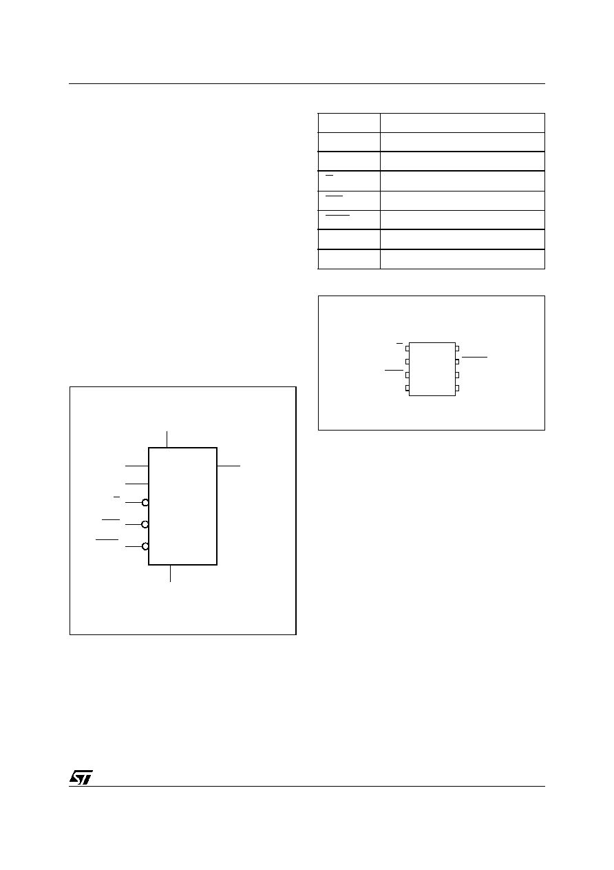
Figure 2. Logic Diagram
Table 1. Signal Names
Figure 3. VDFPN and SO Connections
Note: 1. There is an exposed die paddle on the underside of the
MLP8 package. This is pulled, internally, to V
SS
, and
must not be allowed to be connected to any other voltage
or signal line on the PCB.
2. See
PACKAGE MECHANICAL
section for package di-
mensions, and how to identify pin-1.
Reset
AI10779
S
VCC
M25PE80
VSS
TSL
Q
C
D
C Serial
Clock
D
Serial Data Input
Q
Serial Data Output
S
Chip Select
TSL
Top Sector Lock
Reset Reset
V
CC
Supply Voltage
V
SS
Ground
1
AI10780
2
3
4
8
7
6
5
D
VSS
C
Reset
Q
S
VCC
TSL
M25PE80