1/16
August 2002
M27C256B
256 Kbit (32Kb x 8) UV EPROM and OTP EPROM
s
5V ± 10% SUPPLY VOLTAGE in READ
OPERATION
s
ACCESS TIME: 45ns
s
LOW POWER CONSUMPTION:
≠ Active Current 30mA at 5MHz
≠ Standby Current 100µA
s
PROGRAMMING VOLTAGE: 12.75V ± 0.25V
s
PROGRAMMING TIME: 100µs/word
s
ELECTRONIC SIGNATURE
≠ Manufacturer Code: 20h
≠ Device Code: 8Dh
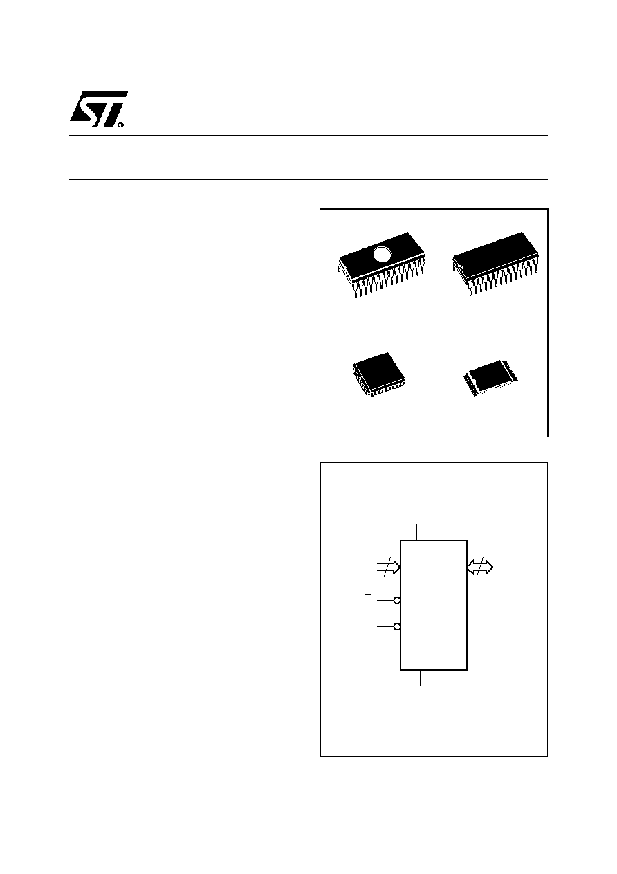
DESCRIPTION
The M27C256B is a 256 Kbit EPROM offered in
the two ranges UV (ultra violet erase) and OTP
(one time programmable). It is ideally suited for mi-
croprocessor systems and is organized as 32,768
by 8 bits.
The FDIP28W (window ceramic frit-seal package)
has a transparent lid which allows the user to ex-
pose the chip to ultraviolet light to erase the bit pat-
tern. A new pattern can then be written to the
device by following the programming procedure.
For applications where the content is programmed
only one time and erasure is not required, the
M27C256B is offered in PDIP28, PLCC32 and
TSOP28 (8 x 13.4 mm) packages.
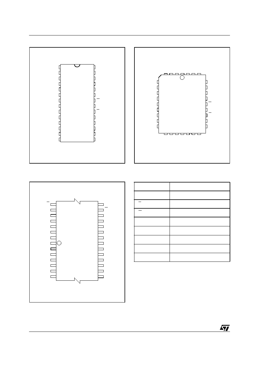
Figure 1. Logic Diagram
AI00755B
15
A0-A14
Q0-Q7
VPP
VCC
M27C256B
G
E
VSS
8
1
28
28
1
FDIP28W (F)
PDIP28 (B)
PLCC32 (C)
TSOP28 (N)
8 x 13.4 mm
M27C256B
2/16
Figure 2B. LCC Connections
AI00757
A13
A8
A10
Q4
17
A0
NC
Q0
Q1
Q2
DU
Q3
A6
A3
A2
A1
A5
A4
9
A14
A9
1
V
PP
A11
Q6
A7
Q7
32
DU
V
CC
M27C256B
A12
NC
Q5
G
E
25
V
SS
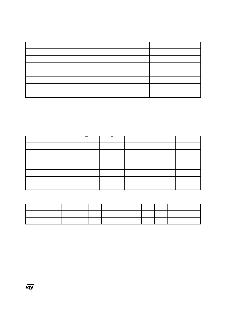
Figure 2A. DIP Connections
A1
A0
Q0
A7
A4
A3
A2
A6
A5
A13
A10
A8
A9
Q7
A14
A11
G
E
Q5
Q1
Q2
Q3
VSS
Q4
Q6
A12
VPP
VCC
AI00756
M27C256B
8
1
2
3
4
5
6
7
9
10
11
12
13
14
16
15
28
27
26
25
24
23
22
21
20
19
18
17
Figure 2C. TSOP Connections
A1
A0
Q0
A5
A2
A4
A3
A9
A11
Q7
A8
G
E
Q5
Q1
Q2
Q3
Q4
Q6
A13
A14
A12
A6
VPP
VCC
A7
AI00614B
M27C256B
28
1
22
7
8
14
15
21
VSS
A10
Table 1. Signal Names
A0-A14
Address Inputs
Q0-Q7
Data Outputs
E
Chip Enable
G
Output Enable
V
PP
Program Supply
V
CC
Supply Voltage
V
SS
Ground
NC
Not Connected Internally
DU
Don't Use
3/16
M27C256B
Table 2. Absolute Maximum Ratings
(1)
Note: 1. Except for the rating "Operating Temperature Range", stresses above those listed in the Table "Absolute Maximum Ratings" may
cause permanent damage to the device. These are stress ratings only and operation of the device at these or any other conditions
above those indicated in the Operating sections of this specification is not implied. Exposure to Absolute Maximum Rating condi-
tions for extended periods may affect device reliability. Refer also to the STMicroelectronics SURE Program and other relevant qual-
ity documents.
2. Minimum DC voltage on Input or Output is ≠0.5V with possible undershoot to ≠2.0V for a period less than 20ns. Maximum DC
voltage on Output is V
CC
+0.5V with possible overshoot to V
CC
+2V for a period less than 20ns.
3. Depends on range.
Table 3. Operating Modes
Note: X = V
IH
or V
IL
, V
ID
= 12V ± 0.5V.
Table 4. Electronic Signature
Symbol
Parameter
Value
Unit
T
A
Ambient Operating Temperature
(3)
≠40 to 125
∞C
T
BIAS
Temperature Under Bias
≠50 to 125
∞C
T
STG
Storage Temperature
≠65 to 150
∞C
V
IO
(2)
Input or Output Voltage (except A9)
≠2 to 7
V
V
CC
Supply Voltage
≠2 to 7
V
V
A9
(2)
A9 Voltage
≠2 to 13.5
V
V
PP
Program Supply Voltage
≠2 to 14
V
Mode
E
G
A9
V
PP
Q7-Q0
Read
V
IL
V
IL
X
V
CC
Data Out
Output Disable
V
IL
V
IH
X
V
CC
Hi-Z
Program
V
IL
Pulse
V
IH
X
V
PP
Data In
Verify
V
IH
V
IL
X
V
PP
Data Out
Program Inhibit
V
IH
V
IH
X
V
PP
Hi-Z
Standby
V
IH
X
X
V
CC
Hi-Z
Electronic Signature
V
IL
V
IL
V
ID
V
CC
Codes
Identifier
A0
Q7
Q6
Q5
Q4
Q3
Q2
Q1
Q0
Hex Data
Manufacturer's Code
V
IL
0
0
1
0
0
0
0
0
20h
Device Code
V
IH
1
0
0
0
1
1
0
1
8Dh

M27C256B
4/16
DEVICE OPERATION
The operating modes of the M27C256B are listed
in the Operating Modes. A single power supply is
required in the read mode. All inputs are TTL lev-
els except for V
PP
and 12V on A9 for Electronic
Signature.
Read Mode
The M27C256B has two control functions, both of
which must be logically active in order to obtain
data at the outputs. Chip Enable (E) is the power
control and should be used for device selection.
Output Enable (G) is the output control and should
be used to gate data to the output pins, indepen-
dent of device selection. Assuming that the ad-
dresses are stable, the address access time
(t
AVQV
) is equal to the delay from E to output
(t
ELQV
). Data is available at the output after delay
of t
GLQV
from the falling edge of G, assuming that
E has been low and the addresses have been sta-
ble for at least t
AVQV
-t
GLQV
.
Standby Mode
The M27C256B has a standby mode which reduc-
es the supply current from 30mA to 100µA. The
M27C256B is placed in the standby mode by ap-
plying a CMOS high signal to the E input. When in
the standby mode, the outputs are in a high imped-
ance state, independent of the G input.
Table 5. AC Measurement Conditions
High Speed
Standard
Input Rise and Fall Times
10ns
20ns
Input Pulse Voltages
0 to 3V
0.4V to 2.4V
Input and Output Timing Ref. Voltages
1.5V
0.8V and 2V
Figure 3. AC Testing Input Output Waveform
AI01822
3V
High Speed
0V
1.5V
2.4V
Standard
0.4V
2.0V
0.8V
Figure 4. AC Testing Load Circuit
AI01823B
1.3V
OUT
CL
CL = 30pF for High Speed
CL = 100pF for Standard
CL includes JIG capacitance
3.3k
1N914
DEVICE
UNDER
TEST
Table 6. Capacitance
(1)
(T
A
= 25 ∞C, f = 1 MHz)
Note: 1. Sampled only, not 100% tested.
Symbol
Parameter
Test Condition
Min
Max
Unit
C
IN
Input Capacitance
V
IN
= 0V
6
pF
C
OUT
Output Capacitance
V
OUT
= 0V
12
pF
5/16
M27C256B
Table 7. Read Mode DC Characteristics
(1)
(T
A
= 0 to 70∞C, ≠40 to 85∞C, ≠40 to 105∞C or ≠40 to 125∞C; V
CC
= 5V ± 5% or 5V ± 10%; V
PP
= V
CC
)
Note: 1. V
CC
must be applied simultaneously with or before V
PP
and removed simultaneously or after V
PP
.
2. Maximum DC voltage on Output is V
CC
+0.5V.
Table 8A. Read Mode AC Characteristics
(1)
(T
A
= 0 to 70∞C, ≠40 to 85∞C, ≠40 to 105∞C or ≠40 to 125∞C; V
CC
= 5V ± 5% or 5V ± 10%; V
PP
= V
CC
)
Note: 1. V
CC
must be applied simultaneously with or before V
PP
and removed simultaneously or after V
PP
.
2. Sampled only, not 100% tested.
3. Speed obtained with High Speed AC measurement conditions.
Symbol
Parameter
Test Condition
Min
Max
Unit
I
LI
Input Leakage Current
0V
V
IN
V
CC
±10
µA
I
LO
Output Leakage Current
0V
V
OUT
V
CC
±10
µA
I
CC
Supply Current
E = V
IL
, G = V
IL
,
I
OUT
= 0mA, f = 5MHz
30
mA
I
CC1
Supply Current (Standby) TTL
E = V
IH
1
mA
I
CC2
Supply Current (Standby) CMOS
E > V
CC
≠ 0.2V
100
µA
I
PP
Program Current
V
PP
= V
CC
100
µA
V
IL
Input Low Voltage
≠0.3
0.8
V
V
IH
(2)
Input High Voltage
2
V
CC
+ 1
V
V
OL
Output Low Voltage
I
OL
= 2.1mA
0.4
V
V
OH
Output High Voltage TTL
I
OH
= ≠1mA
3.6
V
Output High Voltage CMOS
I
OH
= ≠100µA
V
CC
≠ 0.7V
V
Symbol
Alt
Parameter
Test Condition
M27C256B
Unit
-45
(3)
-60
-70
-80
Min
Max
Min
Max
Min
Max
Min
Max
t
AVQV
t
ACC
Address Valid to
Output Valid
E = V
IL
, G = V
IL
45
60
70
80
ns
t
ELQV
t
CE
Chip Enable Low to
Output Valid
G = V
IL
45
60
70
80
ns
t
GLQV
t
OE
Output Enable Low to
Output Valid
E = V
IL
25
30
35
40
ns
t
EHQZ
(2)
t
DF
Chip Enable High to
Output Hi-Z
G = V
IL
0
25
0
30
0
30
0
30
ns
t
GHQZ
(2)
t
DF
Output Enable High
to Output Hi-Z
E = V
IL
0
25
0
30
0
30
0
30
ns
t
AXQX
t
OH
Address Transition to
Output Transition
E = V
IL
, G = V
IL
0
0
0
0
ns
Two Line Output Control
Because EPROMs are usually used in larger
memory arrays, this product features a 2 line con-
trol function which accommodates the use of mul-
tiple memory connection. The two line control
function allows:
a. the lowest possible memory power dissipation,
b. complete assurance that output bus contention
will not occur.
For the most efficient use of these two control
lines, E should be decoded and used as the prima-
ry device selecting function, while G should be
made a common connection to all devices in the
array and connected to the READ line from the
system control bus. This ensures that all deselect-
ed memory devices are in their low power standby
mode and that the output pins are only active
when data is desired from a particular memory de-
vice.
M27C256B
6/16
Figure 5. Read Mode AC Waveforms
AI00758B
tAXQX
tEHQZ
A0-A14
E
G
Q0-Q7
tAVQV
tGHQZ
tGLQV
tELQV
VALID
Hi-Z
VALID
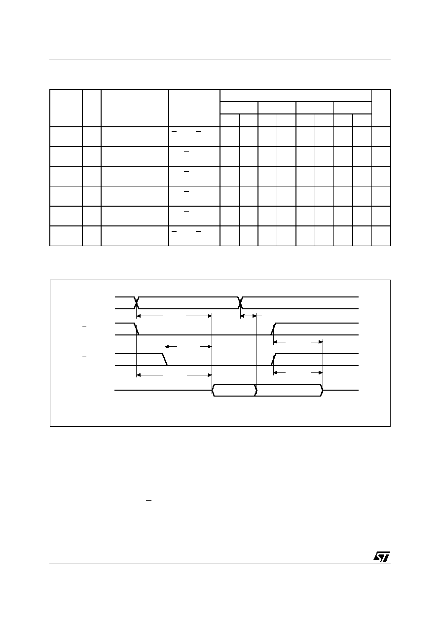
Table 8B. Read Mode AC Characteristics
(1)
(T
A
= 0 to 70∞C, ≠40 to 85∞C, ≠40 to 105∞C or ≠40 to 125∞C; V
CC
= 5V ± 5% or 5V ± 10%; V
PP
= V
CC
)
Note: 1. V
CC
must be applied simultaneously with or before V
PP
and removed simultaneously or after V
PP
.
2. Sampled only, not 100% tested.
Symbol
Alt
Parameter
Test Condition
M27C256B
Unit
-90
-10
-12
-15/-20/-25
Min
Max
Min
Max
Min
Max
Min
Max
t
AVQV
t
ACC
Address Valid to
Output Valid
E = V
IL
, G = V
IL
90
100
120
150
ns
t
ELQV
t
CE
Chip Enable Low to
Output Valid
G = V
IL
90
100
120
150
ns
t
GLQV
t
OE
Output Enable Low to
Output Valid
E = V
IL
40
50
60
65
ns
t
EHQZ
(2)
t
DF
Chip Enable High to
Output Hi-Z
G = V
IL
0
30
0
30
0
40
0
50
ns
t
GHQZ
(2)
t
DF
Output Enable High
to Output Hi-Z
E = V
IL
0
30
0
30
0
40
0
50
ns
t
AXQX
t
OH
Address Transition to
Output Transition
E = V
IL
, G = V
IL
0
0
0
0
ns
System Considerations
The power switching characteristics of Advance
CMOS EPROMs require careful decoupling of the
devices. The supply current, I
CC
, has three seg-
ments that are of interest to the system designer:
the standby current level, the active current level,
and transient current peaks that are produced by
the falling and rising edges of E. The magnitude of
this transient current peaks is dependent on the
capacitive and inductive loading of the device at
the output. The associated transient voltage peaks
can be suppressed by complying with the two line
output control and by properly selected decoupling
capacitors. It is recommended that a 0.1µF ceram-
ic capacitor be used on every device between V
CC
and V
SS
. This should be a high frequency capaci-
tor of low inherent inductance and should be
placed as close to the device as possible. In addi-
tion, a 4.7µF bulk electrolytic capacitor should be
used between V
CC
and V
SS
for every eight devic-
es. The bulk capacitor should be located near the
power supply connection point. The purpose of the
bulk capacitor is to overcome the voltage drop
caused by the inductive effects of PCB traces.
7/16
M27C256B
Table 9. Programming Mode DC Characteristics
(1)
(T
A
= 25 ∞C; V
CC
= 6.25V ± 0.25V; V
PP
= 12.75V ± 0.25V)
Note: V
CC
must be applied simultaneously with or before V
PP
and removed simultaneously or after V
PP
.
Table 10. Programming Mode AC Characteristics
(1)
(T
A
= 25 ∞C; V
CC
= 6.25V ± 0.25V; V
PP
= 12.75V ± 0.25V
Note: V
CC
must be applied simultaneously with or before V
PP
and removed simultaneously or after V
PP
.
Symbol
Parameter
Test Condition
Min
Max
Unit
I
LI
Input Leakage Current
V
IL
V
IN
V
IH
±10
µA
I
CC
Supply Current
50
mA
I
PP
Program Current
E = V
IL
50
mA
V
IL
Input Low Voltage
≠0.3
0.8
V
V
IH
Input High Voltage
2
V
CC
+ 0.5
V
V
OL
Output Low Voltage
I
OL
= 2.1mA
0.4
V
V
OH
Output High Voltage TTL
I
OH
= ≠1mA
3.6
V
V
ID
A9 Voltage
11.5
12.5
V
Symbol
Alt
Parameter
Test Condition
Min
Max
Unit
t
AVEL
t
AS
Address Valid to Chip Enable Low
2
µs
t
QVEL
t
DS
Input Valid to Chip Enable Low
2
µs
t
VPHEL
t
VPS
V
PP
High to Chip Enable Low
2
µs
t
VCHEL
t
VCS
V
CC
High to Chip Enable Low
2
µs
t
ELEH
t
PW
Chip Enable Program Pulse Width
95
105
µs
t
EHQX
t
DH
Chip Enable High to Input Transition
2
µs
t
QXGL
t
OES
Input Transition to Output Enable Low
2
µs
t
GLQV
t
OE
Output Enable Low to Output Valid
100
ns
t
GHQZ
t
DFP
Output Enable High to Output Hi-Z
0
130
ns
t
GHAX
t
AH
Output Enable High to Address Transition
0
ns
Programming
When delivered (and after each erasure for UV
EPROM), all bits of the M27C256B are in the "1"
state. Data is introduced by selectively program-
ming "0"s into the desired bit locations. Although
only "0"s will be programmed, both "1"s and "0"s
can be present in the data word. The only way to
change a '0' to a '1' is by die exposure to ultraviolet
light (UV EPROM). The M27C256B is in the pro-
gramming mode when V
PP
input is at 12.75V, G is
at V
IH
and E is pulsed to V
IL
. The data to be pro-
grammed is applied to 8 bits in parallel to the data
output pins. The levels required for the address
and data inputs are TTL. V
CC
is specified to be
6.25V ± 0.25 V.

M27C256B
8/16
PRESTO II Programming Algorithm
PRESTO II Programming Algorithm allows to pro-
gram the whole array with a guaranteed margin, in
a typical time of 3.5 seconds. Programming with
PRESTO II involves the application of a sequence
of 100µs program pulses to each byte until a cor-
rect verify occurs (see Figure 7). During program-
ming and verify operation, a MARGIN MODE
circuit is automatically activated in order to guar-
antee that each cell is programmed with enough
margin. No overprogram pulse is applied since the
verify in MARGIN MODE provides necessary mar-
gin to each programmed cell.
Program Inhibit
Programming of multiple M27C256Bs in parallel
with different data is also easily accomplished. Ex-
cept for E, all like inputs including G of the parallel
M27C256B may be common. A TTL low level
pulse applied to a M27C256B's E input, with V
PP
at 12.75V, will program that M27C256B. A high
level E input inhibits the other M27C256Bs from
being programmed.
Program Verify
A verify (read) should be performed on the pro-
grammed bits to determine that they were correct-
ly programmed. The verify is accomplished with G
at V
IL
, E at V
IH
, V
PP
at 12.75V and V
CC
at 6.25V.
Figure 6. Programming and Verify Modes AC Waveforms
tAVEL
VALID
AI00759
A0-A14
Q0-Q7
VPP
VCC
G
DATA IN
DATA OUT
E
tQVEL
tVPHEL
tVCHEL
tEHQX
tELEH
tGLQV
tQXGL
tGHQZ
tGHAX
PROGRAM
VERIFY
Figure 7. Programming Flowchart
AI00760B
n = 0
Last
Addr
VERIFY
E = 100
µ
s Pulse
++n
= 25
++ Addr
VCC = 6.25V, VPP = 12.75V
FAIL
CHECK ALL BYTES
1st: VCC = 6V
2nd: VCC = 4.2V
YES
NO
YES
NO
YES
NO

9/16
M27C256B
Electronic Signature
The Electronic Signature (ES) mode allows the
reading out of a binary code from an EPROM that
will identify its manufacturer and type. This mode
is intended for use by programming equipment to
automatically match the device to be programmed
with its corresponding programming algorithm.
The ES mode is functional in the 25∞C ± 5∞C am-
bient temperature range that is required when pro-
gramming the M27C256B. To activate the ES
mode, the programming equipment must force
11.5V to 12.5V on address line A9 of the
M27C256B, with V
CC
= V
PP
= 5V. Two identifier
bytes may then be sequenced from the device out-
puts by toggling address line A0 from V
IL
to V
IH
. All
other address lines must be held at V
IL
during
Electronic Signature mode. Byte 0 (A0 = V
IL
) rep-
resents the manufacturer code and byte 1
(A0 = V
IH
) the device identifier code. For the ST-
Microelectronics M27C256B, these two identifier
bytes are given in Table 4 and can be read-out on
outputs Q7 to Q0.
ERASURE OPERATION (applies for UV EPROM)
The erasure characteristics of the M27C256B is
such that erasure begins when the cells are ex-
posed to light with wavelengths shorter than ap-
proximately 4000 ≈. It should be noted that
sunlight and some type of fluorescent lamps have
wavelengths in the 3000-4000 ≈ range. Research
shows that constant exposure to room level fluo-
rescent lighting could erase a typical M27C256B in
about 3 years, while it would take approximately 1
week to cause erasure when exposed to direct
sunlight. If the M27C256B is to be exposed to
these types of lighting conditions for extended pe-
riods of time, it is suggested that opaque labels be
put over the M27C256B window to prevent unin-
tentional erasure. The recommended erasure pro-
cedure for the M27C256B is exposure to short
wave ultraviolet light which has wavelength
2537≈. The integrated dose (i.e. UV intensity x ex-
posure time) for erasure should be a minimum of
15 W-sec/cm
2
. The erasure time with this dosage
is approximately 15 to 20 minutes using an ultravi-
olet lamp with 12000 µW/cm
2
power rating. The
M27C256B should be placed within 2.5 cm (1
inch) of the lamp tubes during the erasure. Some
lamps have a filter on their tubes which should be
removed before erasure.
M27C256B
10/16
Table 11. Ordering Information Scheme
Note: 1. High Speed, see AC Characteristics section for further information.
For a list of available options (Speed, Package, etc...) or for further information on any aspect of this de-
vice, please contact the STMicroelectronics Sales Office nearest to you.
Example:
M27C256B
-70
X
C
1
TR
Device Type
M27
Supply Voltage
C = 5V
Device Function
256B = 256 Kbit (32Kb x 8)
Speed
-45
(1)
= 45 ns
-60 = 60 ns
-70 = 70 ns
-80 = 80 ns
-90 = 90 ns
-10 = 100 ns
-12 = 120 ns
-15 = 150 ns
-20 = 200 ns
-25 = 250 ns
V
CC
Tolerance
blank = ± 10%
X = ± 5%
Package
F = FDIP28W
B = PDIP28
C = PLCC32
N = TSOP28: 8 x 13.4 mm
Temperature Range
1 = 0 to 70 ∞C
3 = ≠40 to 125 ∞C
6 = ≠40 to 85 ∞C
Options
X = Additional Burn-in
TR = Tape & Reel Packing
11/16
M27C256B
Table 12. Revision History
Date
Version
Revision Details
July 1998
1.0
First Issue
20-Sep-2000
1.1
AN620 Reference removed
29-Nov-2000
1.2
PLCC codification changed (Table 11)
02-Apr-2001
1.3
FDIP28W mechanical dimensions changed (Table 13)
29-Aug-2002
1.4
Package mechanical data clarified for PDIP28 (Table 14),
PLCC32 (Table 15, Figure 10) and TSOP28 (Table 16, Figure 11)
M27C256B
12/16
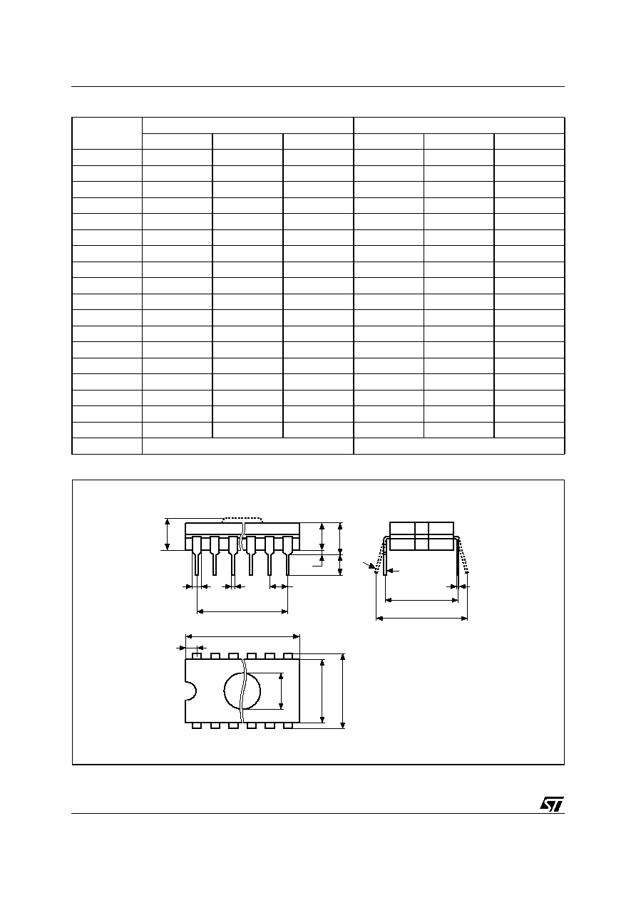
Table 13. FDIP28W - 28 pin Ceramic Frit-seal DIP, with window, Package Mechanical Data
Symbol
millimeters
inches
Typ
Min
Max
Typ
Min
Max
A
5.72
0.225
A1
0.51
1.40
0.020
0.055
A2
3.91
4.57
0.154
0.180
A3
3.89
4.50
0.153
0.177
B
0.41
0.56
0.016
0.022
B1
1.45
≠
≠
0.057
≠
≠
C
0.23
0.30
0.009
0.012
D
36.50
37.34
1.437
1.470
D2
33.02
≠
≠
1.300
≠
≠
E
15.24
≠
≠
0.600
≠
≠
E1
13.06
13.36
0.514
0.526
e
2.54
≠
≠
0.100
≠
≠
eA
14.99
≠
≠
0.590
≠
≠
eB
16.18
18.03
0.637
0.710
L
3.18
4.10
0.125
0.161
S
1.52
2.49
0.060
0.098
7.11
≠
≠
0.280
≠
≠
4∞
11∞
4∞
11∞
N
28
28
Figure 8. FDIP28W - 28 pin Ceramic Frit-seal DIP, with window, Package Outline
Drawing is not to scale.
FDIPW-a
A3
A1
A
L
B1
B
e
D
S
E1
E
N
1
C
eA
D2
eB
A2
13/16
M27C256B
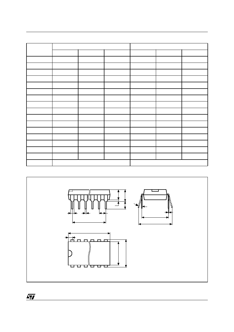
Table 14. PDIP28 - 28 pin Plastic DIP, 600 mils width, Package Mechanical Data
Symbol
millimeters
inches
Typ
Min
Max
Typ
Min
Max
A
4.445
0.1750
A1
0.630
0.0248
A2
3.810
3.050
4.570
0.1500
0.1201
0.1799
B
0.450
0.0177
B1
1.270
0.0500
C
0.230
0.310
0.0091
0.0122
D
36.830
36.580
37.080
1.4500
1.4402
1.4598
D2
33.020
≠
≠
1.3000
≠
≠
E
15.240
0.6000
E1
13.720
12.700
14.480
0.5402
0.5000
0.5701
e1
2.540
≠
≠
0.1000
≠
≠
eA
15.000
14.800
15.200
0.5906
0.5827
0.5984
eB
15.200
16.680
0.5984
0.6567
L
3.300
0.1299
S
1.78
2.08
0.070
0.082
0∞
10∞
0∞
10∞
N
28
28
Figure 9. PDIP28 - 28 pin Plastic DIP, 600 mils width, Package Outline
Drawing is not to scale.
PDIP
A2
A1
A
L
B1
B
e1
D
S
E1
E
N
1
C
eA
eB
D2
M27C256B
14/16
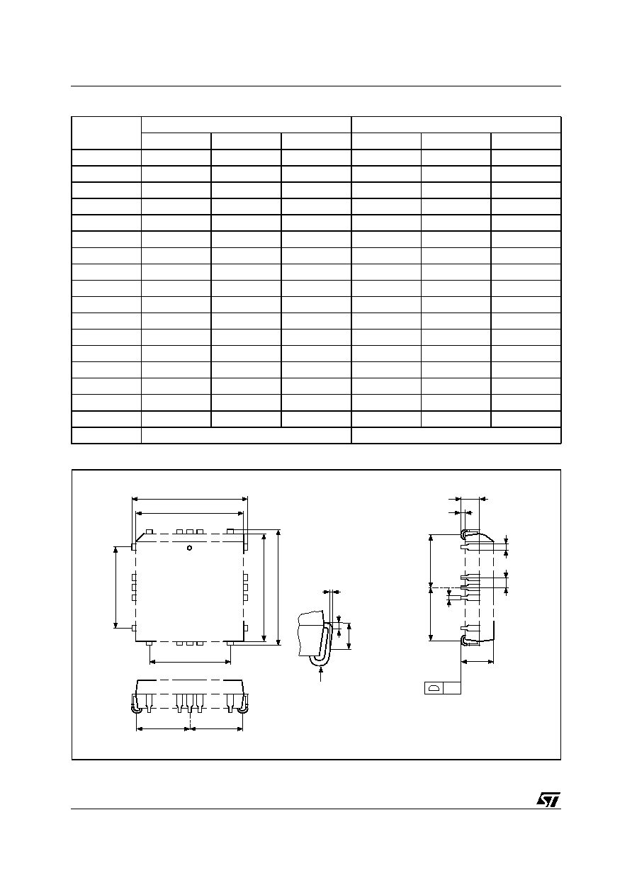
Table 15. PLCC32 - 32 lead Plastic Leaded Chip Carrier, Package Mechanical Data
Symbol
millimeters
inches
Typ
Min
Max
Typ
Min
Max
A
3.18
3.56
0.125
0.140
A1
1.53
2.41
0.060
0.095
A2
0.38
≠
0.015
≠
B
0.33
0.53
0.013
0.021
B1
0.66
0.81
0.026
0.032
CP
0.10
0.004
D
12.32
12.57
0.485
0.495
D1
11.35
11.51
0.447
0.453
D2
4.78
5.66
0.188
0.223
D3
7.62
≠
≠
0.300
≠
≠
E
14.86
15.11
0.585
0.595
E1
13.89
14.05
0.547
0.553
E2
6.05
6.93
0.238
0.273
E3
10.16
≠
≠
0.400
≠
≠
e
1.27
≠
≠
0.050
≠
≠
F
0.00
0.13
0.000
0.005
R
0.89
≠
≠
0.035
≠
≠
N
32
32
Figure 10. PLCC32 - 32 lead Plastic Leaded Chip Carrier, Package Outline
Drawing is not to scale.
PLCC-A
D
E3
E1 E
1 N
D1
D3
CP
B
E2
e
B1
A1
A
R
0.51 (.020)
1.14 (.045)
F
A2
E2
D2
D2
15/16
M27C256B
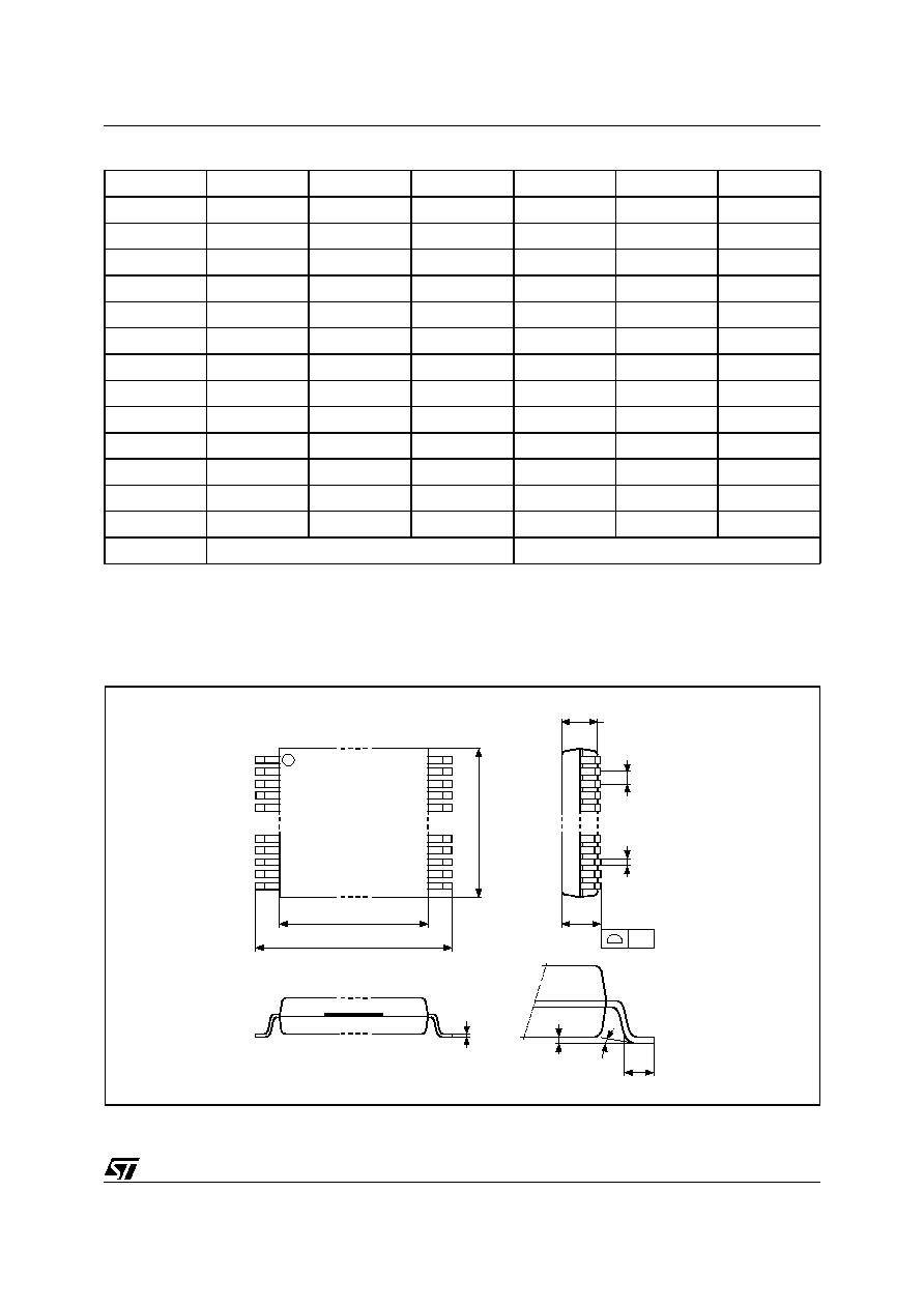
Figure 11. TSOP28 - 28 lead Plastic Thin Small Outline, 8 x 13.4 mm, Package Outline
Drawing is not to scale
TSOP-a
D1
E
1
N
CP
B
e
A2
A
N/2
D
DIE
C
L
A1
Table 16. TSOP28 - 28 lead Plastic Thin Small Outline, 8 x 13.4 mm, Package Mechanical Data
millimeters
inches
Symbol
Typ
Min
Max
Typ
Min
Max
A
1.250
0.0492
A1
0.200
0.0079
A2
0.950
1.150
0.0374
0.0453
B
0.170
0.270
0.0067
0.0106
C
0.100
0.210
0.0039
0.0083
CP
0.100
0.0039
D
13.200
13.600
0.5197
0.5354
D1
11.700
11.900
0.4606
0.4685
e
0.550
≠
≠
0.0217
≠
≠
E
7.900
8.100
0.3110
0.3189
L
0.500
0.700
0.0197
0.0276
0∞
5∞
0∞
5∞
N
28
28

M27C256B
16/16
Information furnished is believed to be accurate and reliable. However, STMicroelectronics assumes no responsibility for the consequences
of use of such information nor for any infringement of patents or other rights of third parties which may result from its use. No license is granted
by implication or otherwise under any patent or patent rights of STMicroelectronics. Specifications mentioned in this publication are subject
to change without notice. This publication supersedes and replaces all information previously supplied. STMicroelectronics products are not
authorized for use as critical components in life support devices or systems without express written approval of STMicroelectronics.
The ST logo is registered trademark of STMicroelectronics
All other names are the property of their respective owners.
© 2002 STMicroelectronics - All Rights Reserved
STMicroelectronics GROUP OF COMPANIES
Australia - Brazil - Canada - China - Finland - France - Germany - Hong Kong - India - Israel - Italy - Japan - Malaysia - Malta -
Morocco - Singapore - Spain - Sweden - Switzerland - United Kingdom - United States
www.st.com