
M27C405
4 Mbit (512Kb x 8) OTP EPROM
March 1999
1/15
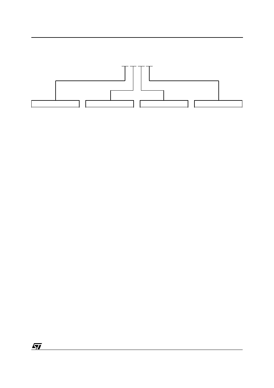
AI01601
19
A0-A18
Q0-Q7
VPP
VCC
M27C405
VSS
8
G
E
Figure 1. Logic Diagram
5V
±
10% SUPPLY VOLTAGE in READ
OPERATION
PIN COMPATIBLE with the 4 Mbit,
SINGLE VOLTAGE FLASH MEMORY
FAST ACCESS TIME: 70ns
LOW POWER CONSUMPTION:
≠ Active Current 30mA at 5MHz
≠ Standby Current 100
µ
A
PROGRAMMING VOLTAGE: 12.75V
±
0.25V
PROGRAMMING TIMES
≠ Typical 48sec. (PRESTO II Algorithm)
≠ Typical 27sec. (On-Board Programming)
ELECTRONIC SIGNATURE
≠ Manufacturer Code: 20h
≠ Device Code: B4
DESCRIPTION
The M27C405 is a 4 Mbit EPROM offered in the
OTP (one time programmable) range. It is ideally
suited for microprocessor systems requiring large
programs, in the application where the contents is
stable and needs to be programmed only one time
and is organised as 524,288 by 8 bits.
The M27C405 is pin compatible with the industry
standard 4 Mbit, single voltage Flash memory. It
can be consideredas a Flash Low Cost solution for
production quantities.
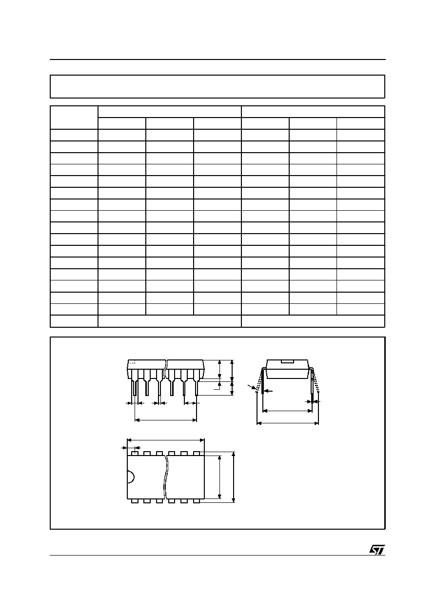
The M27C405 is offered in PDIP32, PLCC32 and
TSOP32 (8 x 20 mm) packages.
A0-A18
Address Inputs
Q0-Q7
Data Outputs
E
Chip Enable
G
Output Enable
V
PP
Program Supply
V
CC
Supply Voltage
V
SS
Ground
Table 1. Signal Names
PLCC32 (K)
32
1
PDIP32 (B)
TSOP32 (N)
8 x 20mm
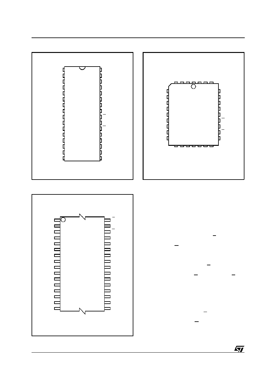
A1
A0
Q0
A7
A4
A3
A2
A6
A5
A13
A10
A8
A9
Q7
A14
A11
G
E
Q5
Q1
Q2
Q3
VSS
Q4
Q6
A17
VPP
A16
A12
A18
VCC
A15
AI01602
M27C405
8
1
2
3
4
5
6
7
9
10
11
12
13
14
15
16
32
31
30
29
28
27
26
25
24
23
22
21
20
19
18
17
Figure 2A. DIP Pin Connections
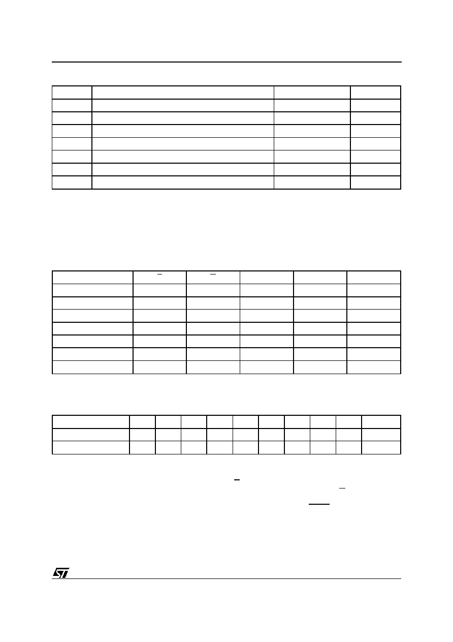
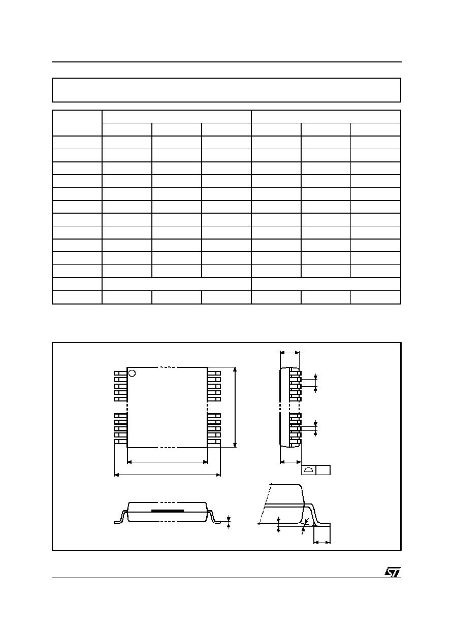
AI01603
A17
A8
A10
Q5
17
A1
A0
Q0
Q1
Q2
Q3
Q4
A7
A4
A3
A2
A6
A5
9
V
PP
A9
1
A16
A11
A13
A12
Q7
32
A18
V
CC
M27C405
A15
A14
Q6
G
E
25
V
SS
Figure 2B. LCC Pin Connections
A1
A0
Q0
A7
A4
A3
A2
A6
A5
A13
A10
A8
A9
Q7
A14
A11
G
E
Q5
Q1
Q2
Q3
Q4
Q6
A17
A18
A16
A12
VPP
VCC
A15
AI01604
M27C405
(Normal)
8
1
9
16
17
24
25
32
VSS
Figure 2C. TSOP Pin Connections
DEVICE OPERATION
The modes of operationsof the M27C405 are listed
in the Operating Modes table. A single power sup-
ply is required in the read mode. All inputs are TTL
levels except for V
pp
and 12V on A9 for Electronic
Signature.
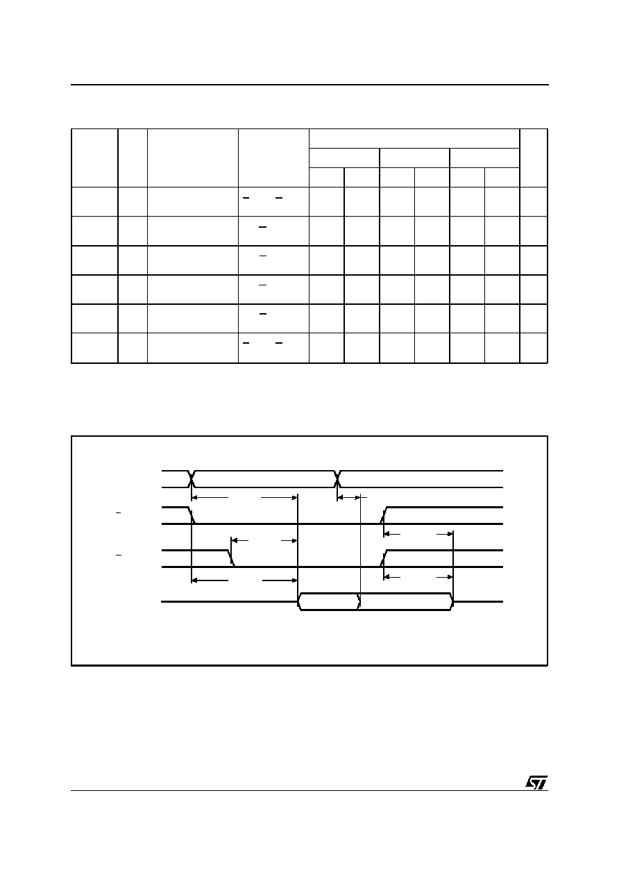
Read Mode
The M27C405 has two control functions, both of
which must be logically active in order to obtain
data at the outputs. Chip Enable (E) is the power
control and should be used for device selection.
Output Enable (G) is the output control and should
be used to gate data to the output pins, inde-
pendent of device selection. Assuming that the
addresses are stable, the address access time
(t
AVQV
) is equalto the delay from E to output (t
ELQV
).
Data is availableat the output after a delay of t
GLQV
from the falling edge of G, assuming that E has
been low and the addresses have been stable for
at least t
AVQV
-t
GLQV
.
Standby Mode
The M27C405 has a standby mode which reduces
the active current from 30mA to 100
µ
A. The
M27C405 is placed in the standby mode by apply-
ing a CMOS high signal to the E input. When in the
standbymode, the outputs are in a high impedance
state, independent of the G input.
2/15
M27C405
Mode
E
G
A9
V
PP
Q0 - Q7
Read
V
IL
V
IL
X
V
CC
or V
SS
Data Out
Output Disable
V
IL
V
IH
X
V
CC
or V
SS
Hi-Z
Program
V
IL
Pulse
V
IH
X
V
PP
Data In
Verify
V
IH
V
IL
X
V
PP
Data Out
Program Inhibit
V
IH
V
IH
X
V
PP
Hi-Z
Standby
V
IH
X
X
V
CC
or V
SS
Hi-Z
Electronic Signature
V
IL
V
IL
V
ID
V
CC
Codes
Note: X = V
IH
or V
IL
, V
ID
= 12V
±
0.5V
Table 3. Operating Modes
Identifier
A0
Q7
Q6
Q5
Q4
Q3
Q2
Q1
Q0
Hex Data
Manufacturer's Code
V
IL
0
0
1
0
0
0
0
0
20h
Device Code
V
IH
1
0
1
1
0
1
0
0
B4h
Table 4. Electronic Signature
Two Line Output Control
Because OTP EPROMs are usually used in larger
memory arrays, this product features a 2 line con-
trol function which accommodates the use of mul-
tiple memory connection. The two line control
function allows:
a. the lowest possible memory power dissipation,
b. complete assurance that output bus contention
will not occur.
For the most efficient use of thesetwo control lines,
E should be decoded and used as the primary
device selecting function, while G should be made
a common connection to all devices in the array
and connected to the READ line from the system
control bus. This ensures that all deselected mem-
ory devices are in their low power standby mode
and that the output pins are only active when data
is required from a particular memory device.
Symbol
Parameter
Value
Unit
T
A
Ambient Operating Temperature
(3)
≠40 to 125
∞
C
T
BIAS
Temperature Under Bias
≠50 to 125
∞
C
T
STG
Storage Temperature
≠65 to 150
∞
C
V
IO
(2)
Input or Output Voltages (except A9)
≠2 to 7
V
V
CC
Supply Voltage
≠2 to 7
V
V
A9
(2)
A9 Voltage
≠2 to 13.5
V
V
PP
Program Supply Voltage
≠2 to 14
V
Notes: 1. Except for the rating "Operating Temperature Range", stresses above those listed in the Table "Absolute Maximum Ratings"
may cause permanent damage to the device. These are stress ratings only and operation of the device at these or any other
conditions above those indicated in the Operating sections of this specification is not implied. Exposure to Absolute Maximum
Rating conditions for extended periods may affect device reliability. Refer also to the STMicroelectronics SURE Program and other
relevant quality documents.
2. Minimum DC voltage on Input or Output is ≠0.5V with possible undershoot to ≠2.0V for a period less than 20ns. Maximum DC
voltage on Output is V
CC
+0.5V with possible overshoot to V
CC
+2V for a period less than 20ns.
3. Depends on range.
Table 2. Absolute Maximum Ratings
(1)
3/15
M27C405
Symbol
Parameter
Test Condition
Min
Max
Unit
C
IN
Input Capacitance
V
IN
= 0V
6
pF
C
OUT
Output Capacitance
V
OUT
= 0V
12
pF
Note: 1. Sampled only, not 100% tested.
Table 6. Capacitance
(1)
(T
A
= 25
∞
C, f = 1 MHz )
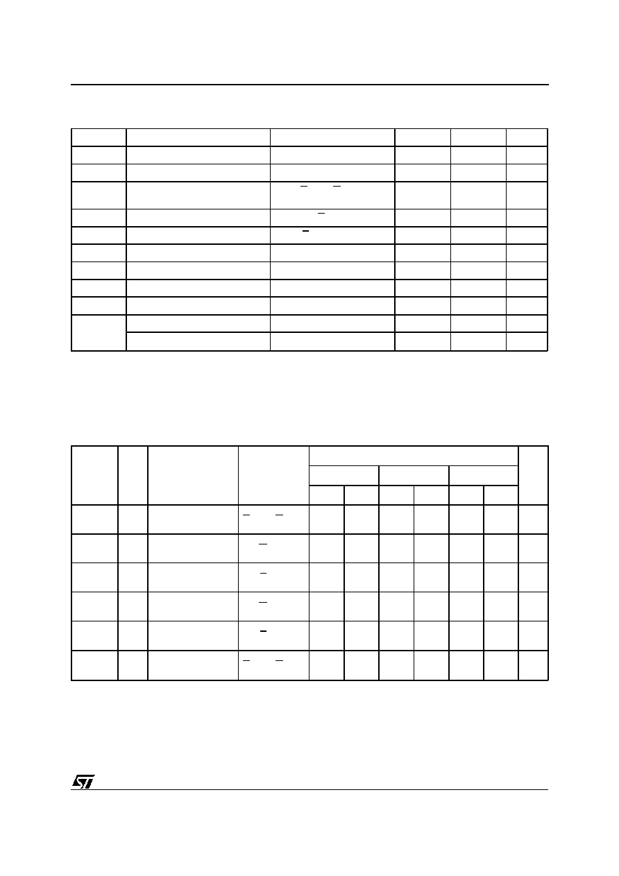
AI01822
3V
High Speed
0V
1.5V
2.4V
Standard
0.4V
2.0V
0.8V
Figure 3. AC Testing Input Output Waveform
AI01823B
1.3V
OUT
CL
CL = 30pF for High Speed
CL = 100pF for Standard
CL includes JIG capacitance
3.3k
1N914
DEVICE
UNDER
TEST
Figure 4. AC Testing Load Circuit
High Speed
Standard
Input Rise and Fall Times
10ns
20ns
Input Pulse Voltages
0 to 3V
0.4V to 2.4V
Input and Output Timing Ref. Voltages
1.5V
0.8V and 2V
Table 5. AC Measurement Conditions
4/15
M27C405
Symbol
Parameter
Test Condition
Min
Max
Unit
I
LI
Input Leakage Current
0V
V
IN
V
CC
±
10
µ
A
I
LO
Output Leakage Current
0V
V
OUT
V
CC
±
10
µ
A
I
CC
Supply Current
E = V
IL
, G = V
IL
,
I
OUT
= 0mA, f = 5MHz
30
mA
I
CC1
Supply Current (Standby) TTL
E = V
IH
1
mA
I
CC2
Supply Current (Standby) CMOS
E > V
CC
≠ 0.2V
100
µ
A
I
PP
Program Current
V
PP
= V
CC
10
µ
A
V
IL
Input Low Voltage
≠0.3
0.8
V
V
IH
(2)
Input High Voltage
2
V
CC
+ 1
V
V
OL
Output Low Voltage
I
OL
= 2.1mA
0.4
V
V
OH
Output High Voltage TTL
I
OH
= ≠400
µ
A
2.4
V
Output High Voltage CMOS
I
OH
= ≠100
µ
A
V
CC
≠ 0.7V
V
Notes: 1. V
CC
must be applied simultaneously with or before V
PP
and removed simultaneously or after V
PP.
2. Maximum DC voltage on Output is V
CC
+0.5V.
Table 7. Read Mode DC Characteristics
(1)
(T
A
= 0 to 70
∞
C or ≠40 to 85
∞
C; V
CC
= 5V
±
10%; V
PP
= V
CC
)
Symbol
Alt
Parameter
Test Condition
M27C405
Unit
-70
(3)
-80
-90
Min
Max
Min
Max
Min
Max
t
AVQV
t
ACC
Address Valid to
Output Valid
E = V
IL
, G = V
IL
70
80
90
ns
t
ELQV
t
CE
Chip Enable Low to
Output Valid
G = V
IL
70
80
90
ns
t
GLQV
t
OE
Output Enable Low
to Output Valid
E = V
IL
35
40
40
ns
t
EHQZ
(2)
t
DF
Chip Enable High to
Output Hi-Z
G = V
IL
0
30
0
30
0
30
ns
t
GHQZ
(2)
t
DF
Output Enable High
to Output Hi-Z
E = V
IL
0
30
0
30
0
30
ns
t
AXQX
t
OH
Address Transition to
Output Transition
E = V
IL
, G = V
IL
0
0
0
ns
Notes: 1. V
CC
must be applied simultaneously with or before V
PP
and removed simultaneously or after V
PP.
2. Sampled only, not 100% tested.
3. In case of 70ns speed see High Speed AC Measurement conditions.
Table 8A. Read Mode AC Characteristics
(1)
(T
A
= 0 to 70
∞
C or ≠40 to 85
∞
C; V
CC
= 5V
±
10%; V
PP
= V
CC
)
5/15
M27C405
Symbol
Alt
Parameter
Test Condition
M27C405
Unit
-100
-120
-150
Min
Max
Min
Max
Min
Max
t
AVQV
t
ACC
Address Valid to
Output Valid
E = V
IL
, G = V
IL
100
120
150
ns
t
ELQV
t
CE
Chip Enable Low to
Output Valid
G = V
IL
100
120
150
ns
t
GLQV
t
OE
Output Enable Low
to Output Valid
E = V
IL
50
60
60
ns
t
EHQZ
(2)
t
DF
Chip Enable High to
Output Hi-Z
G = V
IL
0
30
0
40
0
50
ns
t
GHQZ
(2)
t
DF
Output Enable High
to Output Hi-Z
E = V
IL
0
30
0
40
0
50
ns
t
AXQX
t
OH
Address Transition to
Output Transition
E = V
IL
, G = V
IL
0
0
0
ns
Notes: 1. V
CC
must be applied simultaneously with or before V
PP
and removed simultaneously or after V
PP.
2. Sampled only, not 100% tested.
Table 8B. Read Mode AC Characteristics
(1)
(T
A
= 0 to 70
∞
C or ≠40 to 85
∞
C; V
CC
= 5V
±
10%; V
PP
= V
CC
)
AI00724B
tAXQX
tEHQZ
A0-A18
E
G
Q0-Q7
tAVQV
tGHQZ
tGLQV
tELQV
VALID
Hi-Z
VALID
Figure 5. Read Mode AC Waveforms
6/15
M27C405
Symbol
Parameter
Test Condition
Min
Max
Unit
I
LI
Input Leakage Current
0
V
IN
V
CC
±
10
µ
A
I
CC
Supply Current
50
mA
I
PP
Program Current
E = V
IL
50
mA
V
IL
Input Low Voltage
≠0.3
0.8
V
V
IH
Input High Voltage
2
V
CC
+ 0.5
V
V
OL
Output Low Voltage
I
OL
= 2.1mA
0.4
V
V
OH
Output High Voltage TTL
I
OH
= ≠400
µ
A
2.4
V
V
ID
A9 Voltage
11.5
12.5
V
Note: 1. V
CC
must be applied simultaneously with or before V
PP
and removed simultaneously or after V
PP
.
Table 9. Programming Mode DC Characteristics
(1)
(T
A
= 25
∞
C; V
CC
= 6.25V
±
0.25V; V
PP
= 12.75V
±
0.25V)
Symbol
Alt
Parameter
Test Condition
Min
Max
Unit
t
AVEL
t
AS
Address Valid to Chip Enable Low
2
µ
s
t
QVEL
t
DS
Input Valid to Chip Enable Low
2
µ
s
t
VPHEL
t
VPS
V
PP
High to Chip Enable Low
2
µ
s
t
VCHEL
t
VCS
V
CC
High to Chip Enable Low
2
µ
s
t
ELEH
t
PW
Chip Enable Program Pulse
Width
95
105
µ
s
t
EHQX
t
DH
Chip Enable High to Input
Transition
2
µ
s
t
QXGL
t
OES
Input Transition to Output Enable
Low
2
µ
s
t
GLQV
t
OE
Output Enable Low to Output
Valid
100
ns
t
GHQZ
t
DFP
Output Enable High to Output
Hi-Z
0
130
ns
t
GHAX
t
AH
Output Enable High to Address
Transition
0
ns
Notes: 1. V
CC
must be applied simultaneously with or before V
PP
and removed simultaneously or after V
PP
.
2. Sampled only, not 100% tested.
Table 10. Programming Mode AC Characteristics
(1)
(T
A
= 25
∞
C; V
CC
= 6.25V
±
0.25V; V
PP
= 12.75V
±
0.25V)
7/15
M27C405
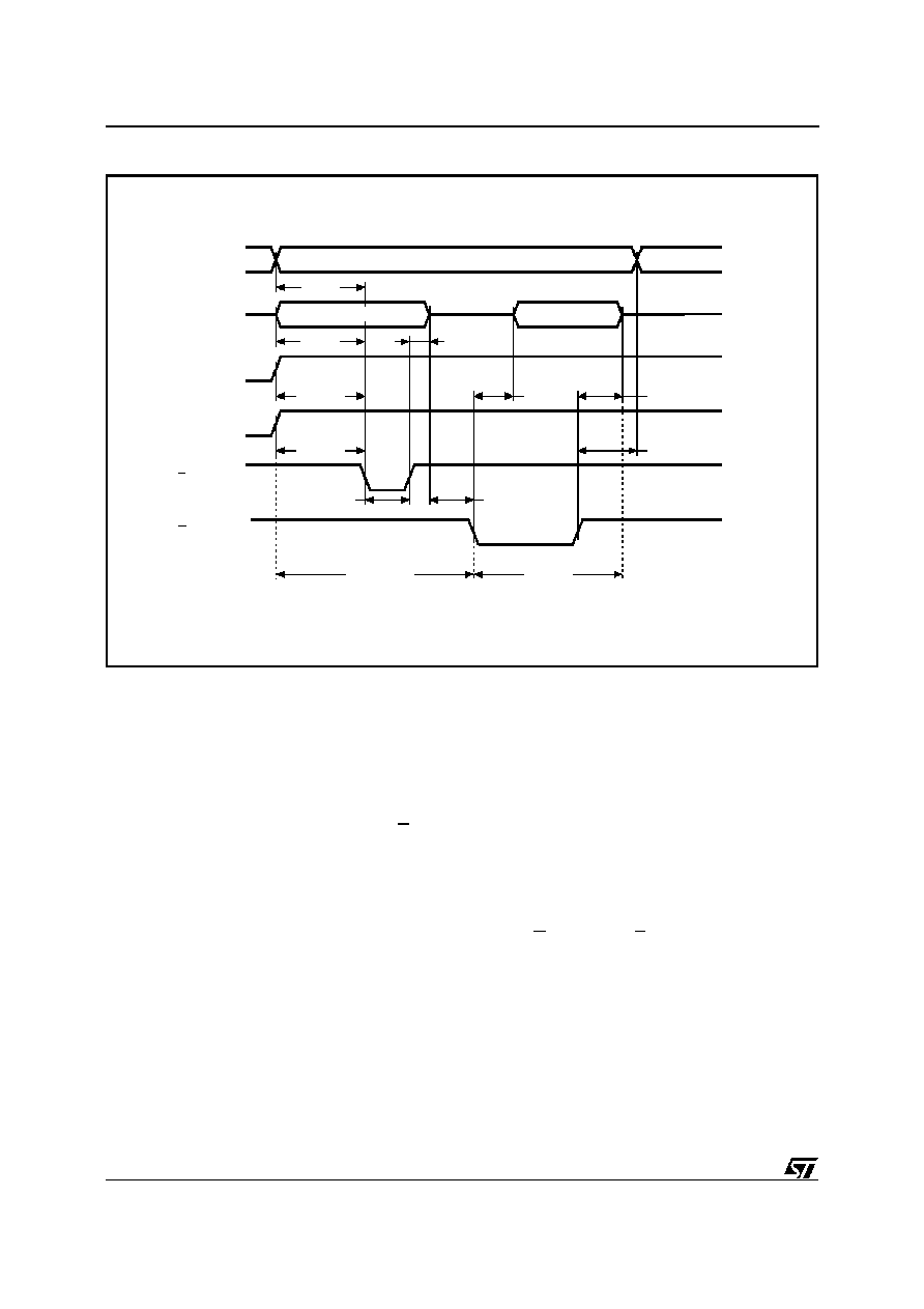
tAVPL
VALID
AI00725
A0-A18
Q0-Q7
VPP
VCC
G
DATA IN
DATA OUT
E
tQVEL
tVPHEL
tVCHEL
tEHQX
tELEH
tGLQV
tQXGL
tGHQZ
tGHAX
PROGRAM
VERIFY
Figure 6. Programming and Verify Modes AC Waveforms
System Considerations
The power switching characteristics of Advanced
CMOS OTP EPROMs require careful decoupling of
the devices. The supply current, I
CC
, has three
segments that are of interest to the system de-
signer : the standby current level, the active current
level, and transient current peaks that are pro-
duced by the falling and rising edges of E. The
magnitude of the transient current peaks is de-
pendent on the capacitive and inductive loading of
the device at the output.
The associated transient voltage peaks can be
suppressed by complying with the two line output
control and by properly selected decoupling ca-
pacitors. It is recommended that a 0.1
µ
F ceramic
capacitor be used on every device between V
CC
and V
SS
. This should be a high frequency capacitor
of low inherent inductance and should be placed
as close to the device as possible. In addition, a
4.7
µ
F bulk electrolytic capacitor should be used
between V
CC
and V
SS
for every eight devices. The
bulk capacitor should be located near the power
supply connection point.The purpose of the bulk
capacitor is to overcome the voltage drop caused
by the inductive effects of PCB traces.
Programming
When delivered, all bits of the M27C405 are in the
'1' state. Data is introducedby selectively program-
ming '0's into the desired bit locations. Although
only '0's will be programmed, both '1's and '0's can
be present in the data word. The M27C405 is in
the programming mode when V
PP
input is at
12.75V,G is at V
IH
and E is pulsed to V
IL
. The data
to be programmed is applied to 8 bits in parallel to
the data output pins. The levels required for the
address and data inputs are TTL. V
CC
is specified
to be 6.25V
±
0.25V.
8/15
M27C405
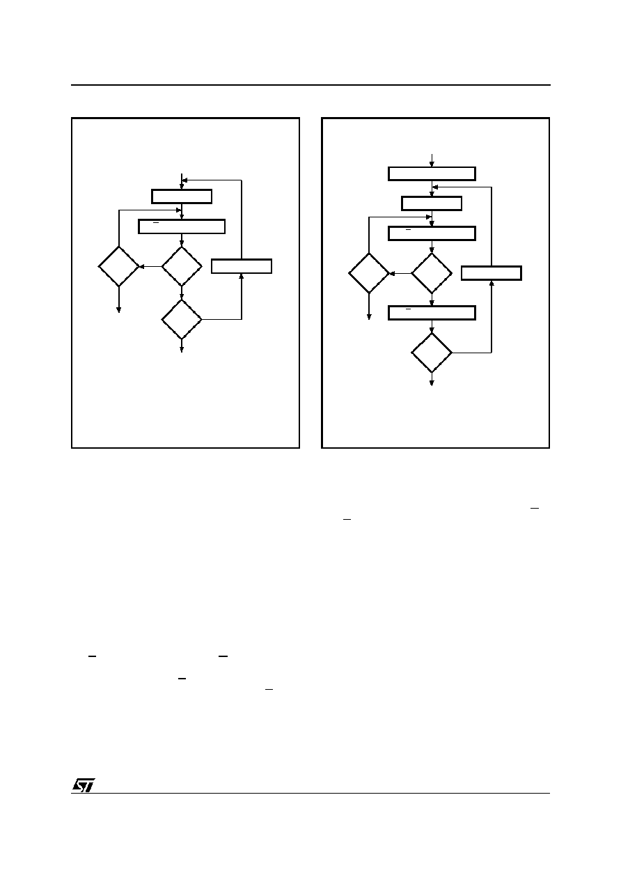
AI00760B
n = 0
Last
Addr
VERIFY
E = 100
µ
s Pulse
++n
= 25
++ Addr
VCC = 6.25V, VPP = 12.75V
FAIL
CHECK ALL BYTES
1st: VCC = 6V
2nd: VCC = 4.2V
YES
NO
YES
NO
YES
NO
Figure 7. Programming Flowchart
PRESTO II Programming Algorithm
PRESTO II Programming Algorithm allows the
whole array to be programmed with a guaranteed
margin, in a typical time of 52.5 seconds.Program-
ming with PRESTO II consists of applying a se-
quence of 100
µ
s program pulses to each byte until
a correct verify occurs (see Figure 7). During pro-
gramming and verify operation, a MARGIN MODE
circuit is automaticallyactivated in order to guaran-
tee that each cell is programmed with enough
margin. No overprogram pulse is applied since the
verify in MARGIN MODE provides the necessary
margin to each programmed cell.
Program Inhibit
Programming of multiple M27C405s in parallel with
different data is also easily accomplished. Except
for E, all like inputs including G of the parallel
M27C405 may be common. A TTL low level pulse
appliedto a M27C405'sE input,with V
PP
at 12.75V,
will program that M27C405. A high level E input
inhibits the other M27C405s from being pro-
grammed.
Program Verify
A verify (read) should be performed on the pro-
grammed bits to determine that they were correctly
programmed. The verify is accomplished with G at
V
IL
, E at V
IH
, V
PP
at 12.75V and V
CC
at 6.25V.
On-Board Programming
Programming the M27C405 may be performed
directly in the application circuit, however this re-
quires modification to the PRESTO II Algorithm
(see Figure 8). For in-circuit programming V
CC
is
determined by the user and normally is compatible
with other components using the same supply volt-
age. It is recommended that the maximum value of
V
CC
which remains compatible with the circuit is
used.
Typically V
CC
=5.5V for programming systems us-
ing V
CC
=5V is recommended. The value of V
CC
does not affect the programming, it gives a higher
test capability in VERIFY mode.
V
PP
must be kept at 12.75 volts to maintain and
enable the programming.
AI01349
n = 0
Last
Addr
VERIFY
?
E = 10
µ
s Pulse
++n
= 25
++ Addr
VPP = 12.75V
FAIL
CHECK ALL BYTES
VPP = VCC
YES
NO
YES
NO
YES
NO
SET MARGIN MODE
E = 10
µ
s Pulse
Figure 8. On-Board Programming Flowchart
9/15
M27C405

Warning: compatibility with FLASH Memory
Compatibility issues may arise when replacing the
compatible Single Supply 4 Megabit FLASH Mem-
ory (the M29F040) by the M27C405.
The V
PP
pin of the M27C405 corresponds to the
"W" pin of the M29F040. The M27C405 V
PP
pin can
withstand voltages up to 12.75V, while the "W" pin
of the M29F040 is a normal control signal input and
may be damaged if a high voltage is applied;
special precautions must be taken when program-
ming in-circuit.
However if an already programmed M27C405 is
used, this can be directly put in place of the FLASH
Memoryas the V
PP
input,when not in programming
mode, is set to V
CC
or V
SS
.
Changes to PRESTO II. The duration of the pro-
gramming pulse is reduced to 20
µ
s, making the
programming time of the M27C405 comparable
with the counterpart FLASH Memory.
Electronic Signature
The Electronic Signature (ES) mode allows the
reading out of a binary code from an OTP EPROM
that will identify its manufacturer and type. this
mode is intended for use by programming equip-
ment to automatically match the device to be pro-
grammed with its corresponding programming
algorithm. This mode is functionalin the 25
∞
C
±
5
∞
C
ambient temperature range that is required when
programming the M27C405. To activate the ES
mode, the programming equipment must force
11.5V to 12.5V on address line A9 of the M27C405
with V
PP
=V
CC
=5V. Two identifier bytes may then be
sequenced from the device outputs by toggling
address line A0 from V
IL
to V
IH
. All other address
lines must be held at V
IL
during Electronic Signa-
ture mode. Byte 0 (A0=V
IL
) represents the manu-
facturer code and byte 1 (A0=V
IH
) the device
identifier code. For the STMicroelectronics
M27C405, these two identifier bytes are given in
Table 4 and can be read-out on outputs Q0 to Q7.
10/15
M27C405
ORDERING INFORMATION SCHEME
Note: 1. High Speed, see AC Characteristics section for further information.
For a list of available options (Speed, Package, etc...) or for further information on any aspect of this device,
please contact the STMicroelectronics Sales Office nearest to you.
Speed
-70
(1)
70 ns
-80
80 ns
-90
90 ns
-100
100 ns
-120
120 ns
-150
150 ns
Package
B
PDIP32
K
PLCC32
N
TSOP32
8 x 20mm
Temperature Range
1
0 to 70
∞
C
6
≠40 to 85
∞
C
Option
TR
Tape & Reel
Packing
Example:
M27C405
-80 K
1 TR
11/15
M27C405
PDIP32 - 32 pin Plastic DIP, 600 mils width
PDIP
A2
A1
A
L
B1
B
e1
D
S
E1
E
N
1
C
eA
eB
D2
Symb
mm
inches
Typ
Min
Max
Typ
Min
Max
A
≠
5.08
≠
0.200
A1
0.38
≠
0.015
≠
A2
3.56
4.06
0.140
0.160
B
0.38
0.51
0.015
0.020
B1
1.52
≠
≠
0.060
≠
≠
C
0.20
0.30
0.008
0.012
D
41.78
42.04
1.645
1.655
D2
38.10
≠
≠
1.500
≠
≠
E
15.24
≠
≠
0.600
≠
≠
E1
13.59
13.84
0.535
0.545
e1
2.54
≠
≠
0.100
≠
≠
eA
15.24
≠
0.600
≠
≠
eB
15.24
17.≠78
0.600
0.700
L
3.18
3.43
0.125
0.135
S
1.78
2.03
0.070
0.080
0
∞
10
∞
0
∞
10
∞
N
32
32
Drawing is not to scale.
12/15
M27C405

PLCC32 - 32 lead Plastic Leaded Chip Carrier, rectangular
PLCC
D
Ne
E1 E
1 N
D1
Nd
CP
B
D2/E2
e
B1
A1
A
R
0.51 (.020)
1.14 (.045)
F
A2
Symb
mm
inches
Typ
Min
Max
Typ
Min
Max
A
2.54
3.56
0.100
0.140
A1
1.52
2.41
0.060
0.095
A2
≠
0.38
≠
0.015
B
0.33
0.53
0.013
0.021
B1
0.66
0.81
0.026
0.032
D
12.32
12.57
0.485
0.495
D1
11.35
11.56
0.447
0.455
D2
9.91
10.92
0.390
0.430
E
14.86
15.11
0.585
0.595
E1
13.89
14.10
0.547
0.555
E2
12.45
13.46
0.490
0.530
e
1.27
≠
≠
0.050
≠
≠
F
0.00
0.25
0.000
0.010
R
0.89
≠
≠
0.035
≠
≠
N
32
32
Nd
7
7
Ne
9
9
CP
0.10
0.004
Drawing is not to scale.
13/15
M27C405
TSOP32 - 32 lead Plastic Thin Small Outline, 8 x 20mm
TSOP-a
D1
E
1
N
CP
B
e
A2
A
N/2
D
DIE
C
L
A1
Symb
mm
inches
Typ
Min
Max
Typ
Min
Max
A
1.20
0.047
A1
0.05
0.15
0.002
0.007
A2
0.95
1.05
0.037
0.041
B
0.15
0.27
0.006
0.011
C
0.10
0.21
0.004
0.008
D
19.80
20.20
0.780
0.795
D1
18.30
18.50
0.720
0.728
E
7.90
8.10
0.311
0.319
e
0.50
-
-
0.020
-
-
L
0.50
0.70
0.020
0.028
0
∞
5
∞
0
∞
5
∞
N
32
32
CP
0.10
0.004
Drawing is not to scale.
14/15
M27C405

Information furnished is believed to be accurate and reliable. However, STMicroelectronics assumes no responsibility for the consequences
of use of such information nor for any infringement of patents or other rights of third parties which may result from its use. No license is granted
by implication or otherwise under any patent or patent rights of STMicroelectronics. Spec ifications mentioned in this publication are subject to
change without notice. This publication supersedes and replaces all information previously supplied. STMicroelectronics products are not
authorized for use as critical components in life support devices or systems without express written approval of STMicroelectronics.
The ST logo is a registered trademark of STMicroelectronics
©
1999 STMicroelectronics - All Rights Reserved
STMicroelectronics GROUP OF COMPANIES
Australia - Brazil - Canada - China - France - Germany - Italy - Japan - Korea - Malaysia - Malta - Mexico - Morocco - The Netherlands -
Singapore - Spain - Sweden - Switzerland - Taiwan - Thailand - United Kingdom - U.S.A.
15/15
M27C405