1/15
March 2000
M27W256
256 Kbit (32Kb x 8) Low Voltage UV EPROM and OTP EPROM
s
2.7V to 3.6V SUPPLY VOLTAGE in READ
OPERATION
s
ACCESS TIME:
≠ 70ns at V
CC
= 3.0V to 3.6V
≠ 80ns at V
CC
= 2.7V to 3.6V
s
PIN COMPATIBLE with M27C256B
s
LOW POWER CONSUMPTION:
≠ 15
µ
A max Standby Current
≠ 15mA max Active Current at 5MHz
s
PROGRAMMING TIME 100
µ
s/byte
s
HIGH RELIABILITY CMOS TECHNOLOGY
≠ 2,000V ESD Protection
≠ 200mA Latchup Protection Immunity
s
ELECTRONIC SIGNATURE
≠ Manufacturer Code: 20h
≠ Device Code: 3Dh
DESCRIPTION
The M27W256 is a low voltage 256 Kbit EPROM
offered in the two ranges UV (ultra violet erase)
and OTP (one time programmable). It is ideally
suited for microprocessor systems and is orga-
nized as 32,768 by 8 bits.
The M27W256 operates in the read mode with a
supply voltage as low as 3V. The decrease in op-
erating power allows either a reduction of the size
of the battery or an increase in the time between
battery recharges.
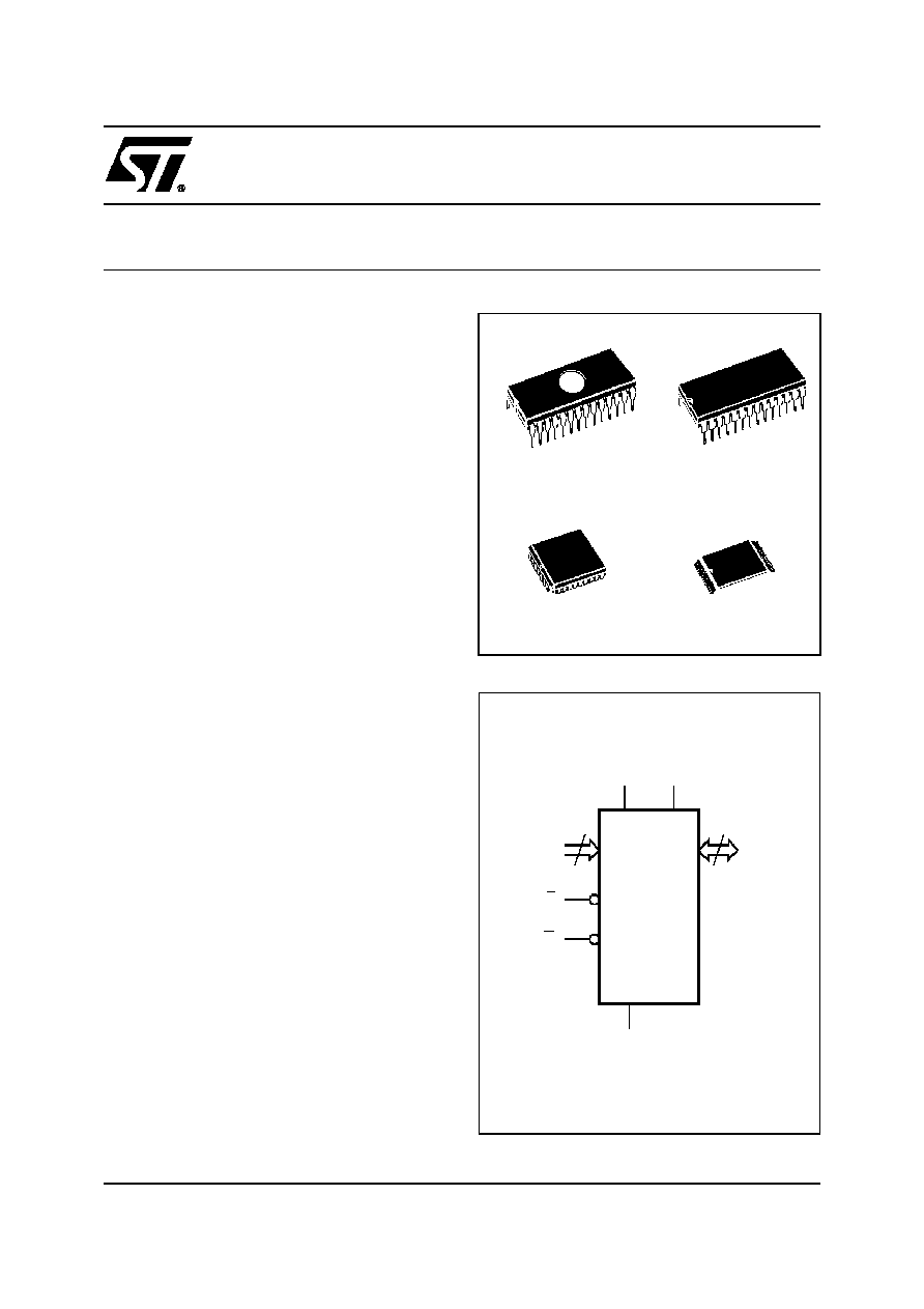
The FDIP28W (window ceramic frit-seal package)
has a transparent lid which allows the user to ex-
pose the chip to ultraviolet light to erase the bit pat-
tern. A new pattern can then be written to the
device by following the programming procedure.
For applications where the content is programmed
only one time and erasure is not required, the
M27W256 is offered in PDIP28, PLCC32 and
TSOP28 (8 x 13.4 mm) packages.
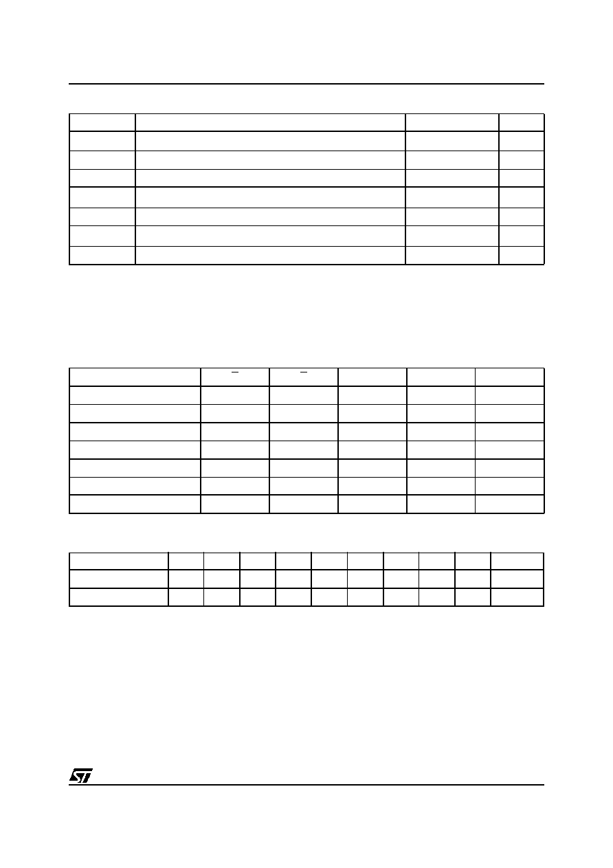
Figure 1. Logic Diagram
AI03629
15
A0-A14
Q0-Q7
VPP
VCC
M27W256
G
E
VSS
8
1
28
28
1
FDIP28W (F)
PDIP28 (B)
PLCC32 (K)
TSOP28 (N)
8 x 13.4mm

M27W256
2/15
Figure 2B. LCC Connections
AI03626
A13
A8
A10
Q4
17
A0
NC
Q0
Q1
Q2
DU
Q3
A6
A3
A2
A1
A5
A4
9
A14
A9
1
V
PP
A11
Q6
A7
Q7
32
DU
V
CC
M27W256
A12
NC
Q5
G
E
25
V
SS
Figure 2A. DIP Connections
A1
A0
Q0
A7
A4
A3
A2
A6
A5
A13
A10
A8
A9
Q7
A14
A11
G
E
Q5
Q1
Q2
Q3
VSS
Q4
Q6
A12
VPP
VCC
AI03627
M27W256
8
1
2
3
4
5
6
7
9
10
11
12
13
14
16
15
28
27
26
25
24
23
22
21
20
19
18
17
Figure 2C. TSOP Connections
A1
A0
Q0
A5
A2
A4
A3
A9
A11
Q7
A8
G
E
Q5
Q1
Q2
Q3
Q4
Q6
A13
A14
A12
A6
VPP
VCC
A7
AI03628
M27W256
28
1
22
7
8
14
15
21
VSS
A10
Table 1. Signal Names
A0-A14
Address Inputs
Q0-Q7
Data Outputs
E
Chip Enable
G
Output Enable
V
PP
Program Supply
V
CC
Supply Voltage
V
SS
Ground
NC
Not Connected Internally
DU
Don't Use
3/15
M27W256
Table 2. Absolute Maximum Ratings
(1)
Note: 1. Except for the rating "Operating Temperature Range", stresses above those listed in the Table "Absolute Maximum Ratings" may
cause permanent damage to the device. These are stress ratings only and operation of the device at these or any other conditions
above those indicated in the Operating sections of this specification is not implied. Exposure to Absolute Maximum Rating condi-
tions for extended periods may affect device reliability. Refer also to the STMicroelectronics SURE Program and other relevant qual-
ity documents.
2. Minimum DC voltage on Input or Output is ≠0.5V with possible undershoot to ≠2.0V for a period less than 20ns. Maximum DC
voltage on Output is V
CC
+0.5V with possible overshoot to V
CC
+2V for a period less than 20ns.
3. Depends on range.
Table 3. Operating Modes
Note: X = V
IH
or V
IL
, V
ID
= 12V
±
0.5V.
Table 4. Electronic Signature
Symbol
Parameter
Value
Unit
T
A
Ambient Operating Temperature
(3)
≠40 to 125
∞
C
T
BIAS
Temperature Under Bias
≠50 to 125
∞
C
T
STG
Storage Temperature
≠65 to 150
∞
C
V
IO
(2)
Input or Output Voltage (except A9)
≠2 to 7
V
V
CC
Supply Voltage
≠2 to 7
V
V
A9
(2)
A9 Voltage
≠2 to 13.5
V
V
PP
Program Supply Voltage
≠2 to 14
V
Mode
E
G
A9
V
PP
Q7-Q0
Read
V
IL
V
IL
X
V
CC
Data Out
Output Disable
V
IL
V
IH
X
V
CC
Hi-Z
Program
V
IL
Pulse
V
IH
X
V
PP
Data In
Verify
V
IH
V
IL
X
V
PP
Data Out
Program Inhibit
V
IH
V
IH
X
V
PP
Hi-Z
Standby
V
IH
X
X
V
CC
Hi-Z
Electronic Signature
V
IL
V
IL
V
ID
V
CC
Codes
Identifier
A0
Q7
Q6
Q5
Q4
Q3
Q2
Q1
Q0
Hex Data
Manufacturer's Code
V
IL
0
0
1
0
0
0
0
0
20h
Device Code
V
IH
1
0
0
0
1
1
0
1
8Dh
M27W256
4/15
DEVICE OPERATION
The modes of operation of the M27W256 are listed
in the Operating Modes. A single power supply is
required in the read mode. All inputs are TTL lev-
els except for V
PP
and 12V on A9 for Electronic
Signature.
Read Mode
The M27W256 has two control functions, both of
which must be logically active in order to obtain
data at the outputs. Chip Enable (E) is the power
control and should be used for device selection.
Output Enable (G) is the output control and should
be used to gate data to the output pins, indepen-
dent of device selection. Assuming that the ad-
dresses are stable, the address access time
(t
AVQV
) is equal to the delay from E to output
(t
ELQV
). Data is available at the output after delay
of t
GLQV
from the falling edge of G, assuming that
E has been low and the addresses have been sta-
ble for at least t
AVQV
-t
GLQV
.
Standby Mode
The M27W256 has a standby mode which reduc-
es the supply current from 10mA to 10
µ
A with low
voltage operation V
CC
3.6V, see Read Mode DC
Characteristics table for details. The M27W256 is
placed in the standby mode by applying a CMOS
high signal to the E input. When in the standby
mode, the outputs are in a high impedance state,
independent of the G input.
Table 5. AC Measurement Conditions
High Speed
Standard
Input Rise and Fall Times
10ns
20ns
Input Pulse Voltages
0 to 3V
0.4V to 2.4V
Input and Output Timing Ref. Voltages
1.5V
0.8V and 2V
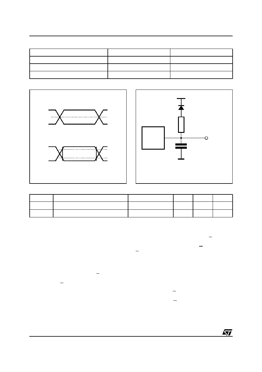
Figure 3. AC Testing Input Output Waveform
AI01822
3V
High Speed
0V
1.5V
2.4V
Standard
0.4V
2.0V
0.8V
Figure 4. AC Testing Load Circuit
AI01823B
1.3V
OUT
CL
CL = 30pF for High Speed
CL = 100pF for Standard
CL includes JIG capacitance
3.3k
1N914
DEVICE
UNDER
TEST
Table 6. Capacitance
(1)
(T
A
= 25
∞
C, f = 1 MHz)
Note: 1. Sampled only, not 100% tested.
Symbol
Parameter
Test Condit ion
Min
Max
Unit
C
IN
Input Capacitance
V
IN
= 0V
6
pF
C
OUT
Output Capacitance
V
OUT
= 0V
12
pF

5/15
M27W256
Table 7. Read Mode DC Characteristics
(1)
(T
A
= ≠40 to 85
∞
C; V
CC
= 2.7V to 3.6V; V
PP
= V
CC
)
Note: 1. V
CC
must be applied simultaneously with or before V
PP
and removed simultaneously or after V
PP
.
2. Maximum DC voltage on Output is V
CC
+0.5V.
Table 8. Read Mode AC Characteristics
(1)
(T
A
= ≠40 to 85
∞
C; V
CC
= 2.7V to 3.6V; V
PP
= V
CC
)
Note: 1. V
CC
must be applied simultaneously with or before V
PP
and removed simultaneously or after V
PP
.
2. Sampled only, not 100% tested.
3. Speed obtained with High Speed AC measurement conditions.
Symbol
Parameter
Test Condition
Min
Max
Unit
I
LI
Input Leakage Current
0V
V
IN
V
CC
±
10
µ
A
I
LO
Output Leakage Current
0V
V
OUT
V
CC
±
10
µ
A
I
CC
Supply Current
E = V
IL
, G = V
IL
,
I
OUT
= 0mA, f = 5MHz,
V
CC
3.6V
15
mA
I
CC1
Supply Current (Standby) TTL
E = V
IH
1
mA
I
CC2
Supply Current (Standby) CMOS
E > V
CC
≠ 0.2V,
V
CC
3.6V
15
µ
A
I
PP
Program Current
V
PP
= V
CC
100
µ
A
V
IL
Input Low Voltage
≠0.6
0.2 V
CC
V
V
IH
(2)
Input High Voltage
0.7 V
CC
V
CC
+ 0.5
V
V
OL
Output Low Voltage
I
OL
= 2.1mA
0.4
V
V
OH
Output High Voltage TTL
I
OH
= ≠400
µ
A
2.4
V
Symbol
Alt
Parameter
Test
Condition
M27W256
Unit
-80
(3)
-100
(-120/-150/-200)
V
CC
= 3.0V to 3.6V V
CC
= 2.7V to 3.6V V
CC
= 2.7V to 3.6V
Min
Max
Min
Max
Min
Max
t
AVQV
t
ACC
Address Valid to
Output Valid
E = V
IL
,
G = V
IL
70
80
100
ns
t
ELQV
t
CE
Chip Enable Low to
Output Valid
G = V
IL
70
80
100
ns
t
GLQV
t
OE
Output Enable Low
to Output Valid
E = V
IL
40
50
60
ns
t
EHQZ
(2)
t
DF
Chip Enable High
to Output Hi-Z
G = V
IL
0
40
0
50
0
60
ns
t
GHQZ
(2)
t
DF
Output Enable High
to Output Hi-Z
E = V
IL
0
40
0
50
0
60
ns
t
AXQX
t
OH
Address Transition
to Output Transition
E = V
IL
,
G = V
IL
0
0
0
ns