
1/23
PRELIMINARY DATA
February 2000
This is preliminary information on a new product now in development or undergoing evaluation. Details are subject to change without notice.
M28010
1 Mbit (128K x 8) Parallel EEPROM
With Software Data Protection
s
Fast Access Time: 100 ns
s
Single Supply Voltage:
≠ 4.5 V to 5.5 V for M28010
≠ 2.7 V to 3.6 V for M28010-W
≠ 1.8 V to 2.4 V for M28010-R
s
Low Power Consumption
s
Fast BYTE and PAGE WRITE (up to 128 Bytes)
s
Enhanced Write Detection and Monitoring:
≠ Data Polling
≠ Toggle Bit
≠ Page Load Timer Status
s
JEDEC Approved Bytewide Pin-Out
s
Software Data Protection
s
Hardware Data Protection
s
Software Chip Erase
s
100000 Erase/Write Cycles (minimum)
s
Data Retention (minimum): 10 Years
DESCRIPTION
The M28010 devices consist of 128Kx8 bits of low
power,
parallel
EEPROM,
fabricated
with
STMicroelectronics' proprietary double polysilicon
CMOS technology. The devices offer fast access
time, with low power dissipation, and require a
single voltage supply (5V, 3V or 2V, depending on
the option chosen).
Figure 1. Logic Diagram
AI02221
17
A0-A16
W
DQ0-DQ7
VCC
M28010
G
E
VSS
8
Table 1. Signal Names
A0-A16
Address Input
DQ0-DQ7
Data Input / Output
W
Write Enable
E
Chip Enable
G
Output Enable
VCC
Supply Voltage
VSS
Ground
PDIP32 (BA)
PLCC32 (KA)
TSOP32 (NA)
8 x 20 mm
32
1

M28010
2/23
Figure 2A. DIP Connections
Note: 1. DU = Do Not Use
Figure 2B. PLCC Connections
Note: 1. DU = Do Not Use
A1
A0
DQ0
A7
A4
A3
A2
A6
A5
A13
A10
A8
A9
DQ7
A14
A11
G
E
DQ5
DQ1
DQ2
DQ3
VSS
DQ4
DQ6
A12
DU
VCC
AI02222
M28010
8
1
15
16
4
5
6
7
9
10
11
12
13
14
32
31
30
27
26
25
24
23
22
21
20
19
18
17
A15
DU
W
A16
2
3
29
28
AI02223
DU
A8
A10
DQ4
17
A0
A7
DQ0
DQ1
DQ2
DQ6
DQ3
A6
A3
A2
A1
A5
A4
9
W
A9
1
A16
A11
A14
A12
DQ7
32
DU
V
CC
M28010
A15
A13
DQ5
G
E
25
V
SS
Figure 2C. TSOP Connections
Note: 1. DU = Do Not Use
A2
A1
A0
A6
A3
A5
A4
A9
A11
DQ7
A8
G
E
DQ5
DQ0
DQ1
DQ3
DQ4
DQ6
A13
W
A15
A7
A14
VCC
A12
AI02224
M28010
8
1
9
16
17
24
25
32
VSS
A10
DQ2
DU
A16
DU
The device has been designed to offer a flexible
microcontroller interface, featuring both hardware
and software hand-shaking, with Data Polling and
Toggle Bit. The device supports a 128 byte Page
Write operation. Software Data Protection (SDP)
is also supported, using the standard JEDEC
algorithm.
The M28010 is designed for applications requiring
as much as 100,000 write cycles and ten years of
data retention. The organization of the data in a 4
byte (32-bit) "word" format leads to significant
savings in power consumption. Once a byte has
been read, subsequent byte read cycles from the
same "word" (with addresses differing only in the
two least significant bits) are fetched from the
previously loaded Read Buffer, not from the
memory array. As a result, the power consumption
for these subsequent read cycles is much lower
than the power consumption for the first cycle. By
careful design of the memory access patterns, a
50% reduction in the power consumption is
possible.
SIGNAL DESCRIPTION
The external connections to the device are
summarized in Table 1, and their use in Table 3.
Addresses (A0-A16). The address inputs are
used to select one byte from the memory array
during a read or write operation.
Data In/Out (DQ0-DQ7). The contents of the data
byte are written to, or read from, the memory array
through the Data I/O pins.
Chip Enable (E). The chip enable input must be
held low to enable read and write operations.
When Chip Enable is high, power consumption is
reduced.
Output Enable (G). The Output Enable input
controls the data output buffers, and is used to
initiate read operations.

3/23
M28010
Figure 3. Block Diagram
AI02225
ADDRESS
LATCH
A7-A16
(Page Address)
X
DECODE
CONTROL
LOGIC
1Mbit ARRAY
ADDRESS
LATCH
A0-A6
I/O BUFFERS
VPP GEN
LATCH PAGE
Y DECODE
SENSE PAGE & DATA LATCH
E
G
W
DQ0-DQ7
ECC
(1)
& MULTIPLEXER
VREAD GEN
REFERENCES
PROGRAMMING
STATE
MACHINE
Table 2. Absolute Maximum Ratings
1
Note: 1. Except for the rating "Operating Temperature Range", stresses above those listed in the Table "Absolute Maximum Ratings" may
cause permanent damage to the device. These are stress ratings only, and operation of the device at these or any other conditions
above those indicated in the Operating sections of this specification is not implied. Exposure to Absolute Maximum Rating condi-
tions for extended periods may affect device reliability. Refer also to the ST SURE Program and other relevant quality documents.
2. MIL-STD-883C, 3015.7 (100 pF, 1500
)
Symbol
Parameter
Value
Unit
T
A
Ambient Operating Temperature
≠40 to 85
∞
C
T
STG
Storage Temperature
≠65 to 150
∞
C
V
CC
Supply Voltage
≠0.3 to V
CCMAX
+1
V
V
IO
Input or Output Voltage (except A9)
≠0.3 to V
CC
+0.6
V
V
I
Input Voltage
≠0.3 to 4.5
V
V
ESD
Electrostatic Discharge Voltage (Human Body model)
2
2000
V
M28010
4/23
Table 3. Operating Modes
1
Note: 1. X = V
IH
or V
IL
.
Mode
E
G
W
DQ0-DQ7
Read
V
IL
V
IL
V
IH
Data Out
Write
V
IL
V
IH
V
IL
Data In
Stand-by / Write Inhibit
V
IH
X
X
Hi-Z
Write Inhibit
X
X
V
IH
Data Out or Hi-Z
Write Inhibit
X
V
IL
X
Data Out or Hi-Z
Output Disable
X
V
IH
X
Hi-Z
Write Enable (W). The Write Enable input controls
whether the addressed location is to be read, from
or written to.
DEVICE OPERATION
In order to prevent data corruption and inadvertent
write operations, an internal V
CC
comparator
inhibits the Write operations if the V
CC
voltage is
lower than V
WI
(see Table 4A to Table 4C). Once
the voltage applied on the V
CC
pin goes over the
V
WI
threshold (V
CC
>V
WI
), write access to the
memory is allowed after a time-out t
PUW
, as
specified in Table 4A to Table 4C.
Further protection against data corruption is
offered by the E and W low pass filters: any glitch,
on the E and W inputs, with a pulse width less than
10 ns (typical) is internally filtered out to prevent
inadvertent write operations to the memory.
Table 4A. Power-Up Timing
1
for M28010 (5V range)
(T
A
= ≠40 to 85
∞
C; V
CC
= 4.5 to 5.5 V)
Note: 1. Sampled only, not 100% tested.
Table 4B. Power-Up Timing
1
for M28010-W (3V range)
(T
A
= ≠40 to 85
∞
C; V
CC
= 2.7 to 3.6 V)
Note: 1. Sampled only, not 100% tested.
Table 4C. Power-Up Timing
1
for M28010-R (2V range)
(T
A
= ≠40 to 85
∞
C; V
CC
= 1.8 to 2.4 V)
Note: 1. Sampled only, not 100% tested.
Symbol
Parameter
Min.
Max.
Unit
t
PUR
Time Delay to Read Operation
5
ms
t
PUW
Time Delay to Write Operation (once V
CC
V
WI
)
5
ms
V
WI
Write Inhibit Threshold
3.0
4.2
V
Symbol
Parameter
Min.
Max.
Unit
t
PUR
Time Delay to Read Operation
5
ms
t
PUW
Time Delay to Write Operation (once V
CC
V
WI
)
5
ms
V
WI
Write Inhibit Threshold
2.0
2.6
V
Symbol
Parameter
Min.
Max.
Unit
t
PUR
Time Delay to Read Operation
5
ms
t
PUW
Time Delay to Write Operation (once V
CC
V
WI
)
5
ms
V
WI
Write Inhibit Threshold
1.2
1.7
V

5/23
M28010
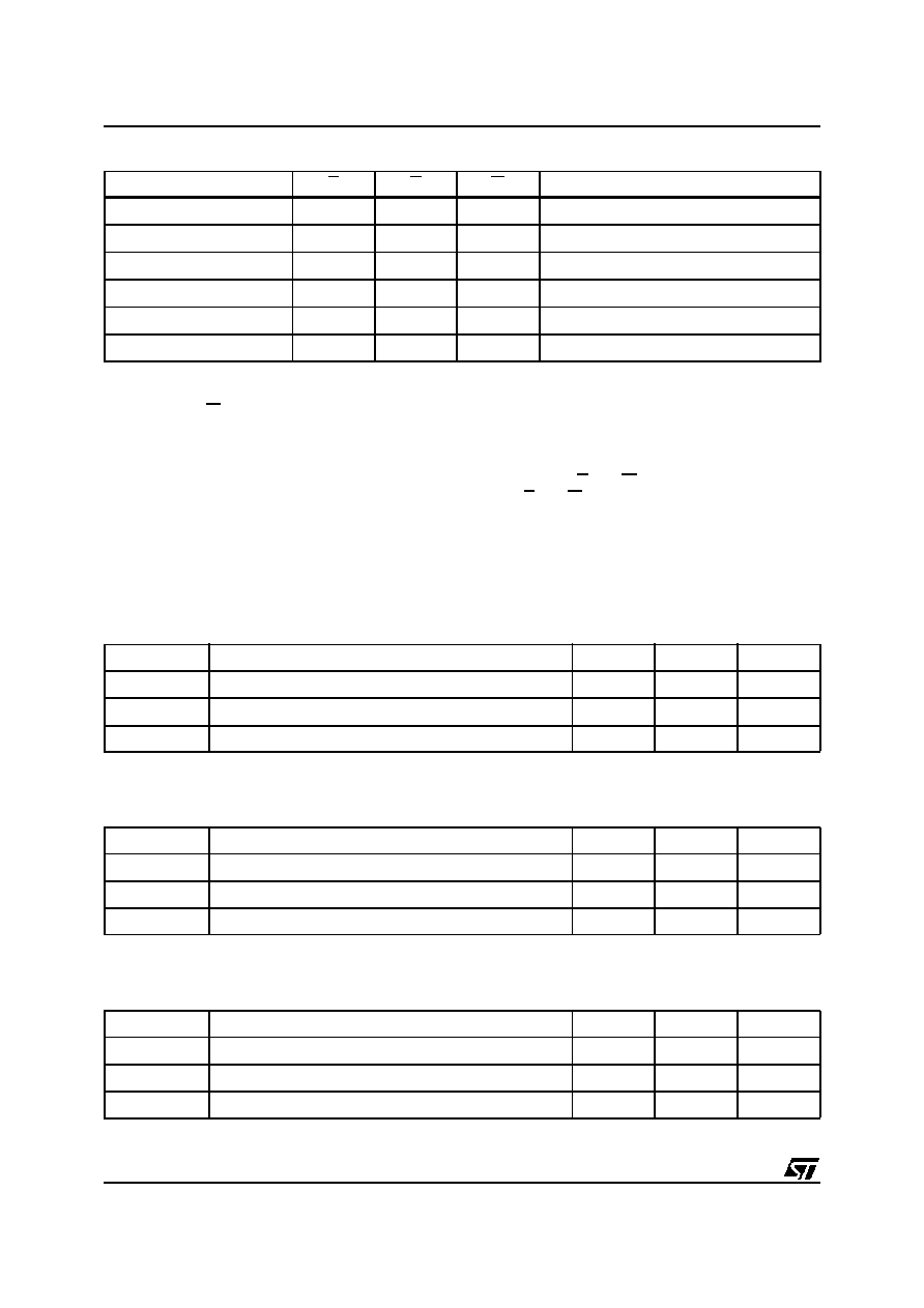
Figure 4. Software Data Protection Enable Algorithms (with or without Memory Write)
Wait for write completion (tQ5HQ5X)
Wait for write completion (tQ5HQ5X)
Wait for write completion (tQ5HQ5X)
AI02227B
Write AAh in
Address 5555h
Write 55h in
Address 2AAAh
Write A0h in
Address 5555h
SDP is set
Page Write
Timing
SDP is Disabled and Application
needs to Enable it, and Write Data
Time Out (tWLQ5H)
DATA has been written
and SDP is Enabled
SDP is Disabled and
Application needs to Enable it
Write AAh in
Address 5555h
Write 55h in
Address 2AAAh
Write A0h in
Address 5555h
Page Write
Timing
DATA has been written
and SDP is Enabled
Time Out (tWLQ5H)
Write data
in any addresses
within one page
Write
is enabled
Write AAh in
Address 5555h
Write 55h in
Address 2AAAh
Write A0h in
Address 5555h
Page Write
Timing
Time Out (tWLQ5H)
Write data
in any addresses
within one page
Write
is enabled
Read
The device is accessed like a static RAM. When E
and G are low, and W is high, the contents of the
addressed location are presented on the I/O pins.
Otherwise, when either G or E is high, the I/O pins
revert to their high impedance state.
Write
Write operations are initiated when both W and E
are low and G is high. The device supports both
W-controlled and E-controlled write cycles (as
shown in Figure 12 and Figure 13). The address is
latched during the falling edge of W or E (which
ever occurs later) and the data is latched on the
rising edge of W or E (which ever occurs first).
After a delay, t
WLQ5H
, that cannot be shorter than
the value specified in Table 9A to Table 9C, the
internal write cycle starts. It continues, under
internal timing control, until the write operation is
complete. The commencement of this period can
be detected by reading the Page Load Timer
Status on DQ5. The end of the internal write cycle
M28010
6/23
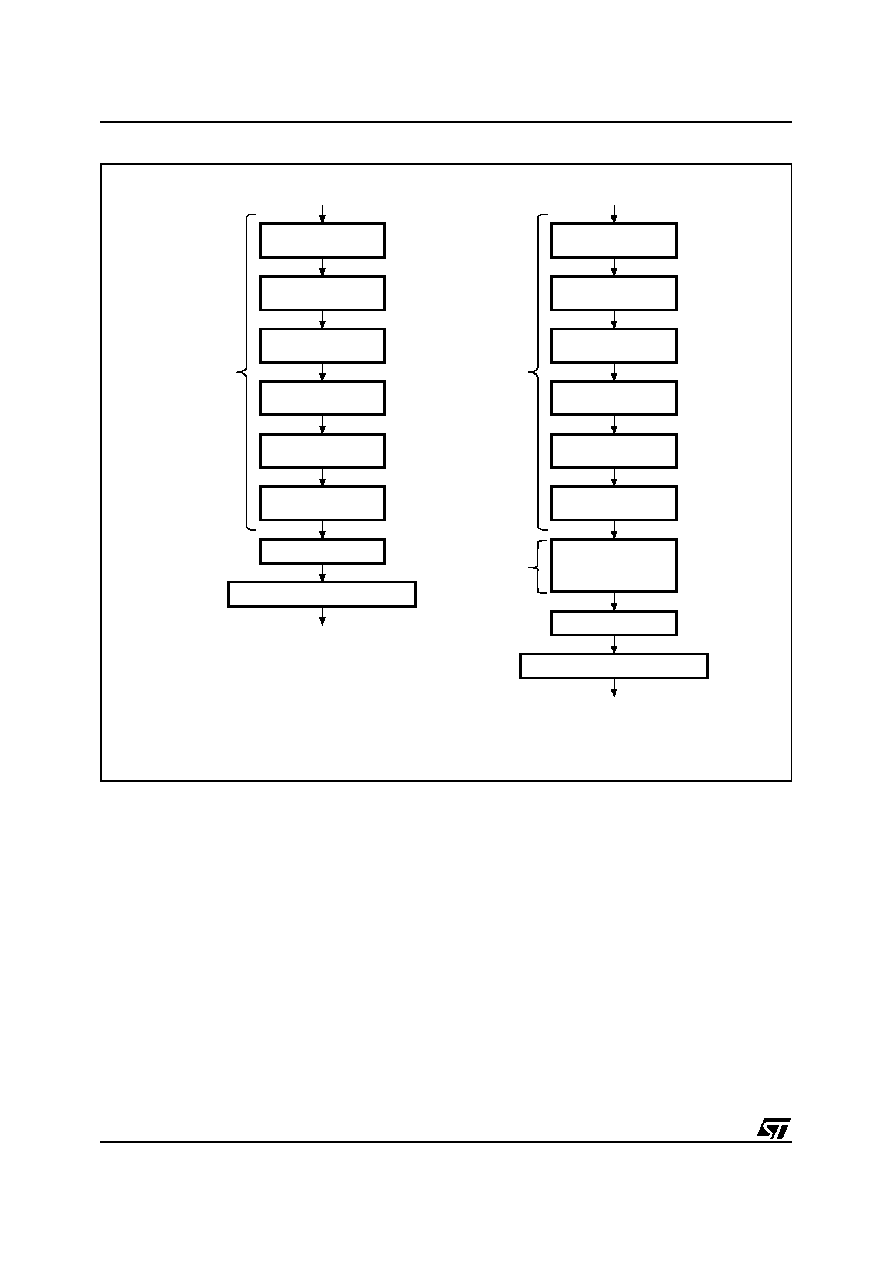
Figure 5. Software Data Protection Disable Algorithms (with or without Memory Write)
Wait for write completion (tQ5HQ5X)
Wait for write completion (tQ5HQ5X)
AI02226B
Write AAh in
Address 5555h
Write 55h in
Address 2AAAh
Write 80h in
Address 5555h
SDP is Disabled
Write AAh in
Address 5555h
Write 55h in
Address 2AAAh
Write 20h in
Address 5555h
Page Write
Timing
SDP is Enabled and
Application needs to Disable it
Time Out (tWLQ5H)
Write AAh in
Address 5555h
Write 55h in
Address 2AAAh
Write 80h in
Address 5555h
DATA has been written
and SDP is Disabled
Write AAh in
Address 5555h
Write 55h in
Address 2AAAh
Write 20h in
Address 5555h
Page Write
Timing
SDP is Enabled and
Application needs to Write Data
Time Out (tWLQ5H)
Write data
in any addresses
within one page
Physical
Write
Instructions
can be detected by reading the status of the Data
Polling and the Toggle Bit functions on DQ7 and
DQ6.
Page Write
The Page Write mode allows up to 128 bytes to be
written on a single page in a single go. This is
achieved through a series of successive Write
operations, no two of which are separated by more
than the t
WLQ5H
value (as specified in Table 9A to
Table 9C).
The page write can be initiated during any byte
write operation. Following the first Byte Write
instruction, the host may send another address
and data with a minimum data transfer rate of:
1/t
WLQ5H
.
The internal write cycle can start at any instant
after t
WLQ5H
. Once initiated, the write operation is
internally timed, and continues, uninterrupted,
until completion.
All bytes must be located on the same page
address (A16-A7 must be the same for all bytes).
Otherwise, the Page Write operation is not
executed. The Page Write Abort event is indicated
to the application via DQ1 (as described on page
8).
As with the single byte Write operation, described
above, the DQ5, DQ6 and DQ7 lines can be used
to detect the beginning and end of the internally
controlled phase of the Page Write cycle.
Software Data Protection (SDP)
The device offers a software-controlled write-
protection mechanism that allows the user to
inhibit all write operations to the device, including
chip erase. This can be useful for protecting the

7/23
M28010
memory from inadvertent write cycles that may
occur during periods of instability (uncontrolled
bus conditions when excessive noise is detected,
or when power supply levels are outside their
specified values).
By
default,
the
device
is
shipped
in
the
"unprotected" state: the memory contents can be
freely changed by the user. Once the Software
Data Protection Mode is enabled, all write
commands are ignored, and have no effect on the
memory contents.
The device remains in this mode until a valid
Software Data Protection disable sequence is
received. The device reverts to its "unprotected"
state.
The status of the Software Data Protection
(enabled or disabled) is represented by a non-
volatile latch, and is remembered across periods
of the power being off.
The Software Data Protection Enable command
consists of the writing of three specific data bytes
to three specific memory locations (each location
being on a different page), as shown in Figure 4.
Similarly, to disable the Software Data Protection,
the user has to write specific data bytes into six
different locations, as shown in Figure 5. This
complex series of operations protects against the
chance of inadvertent enabling or disabling of the
Software Data Protection mechanism.
When SDP is enabled, the memory array can still
have data written to it, but the sequence is more
complex
(and
hence
better
protected
from
inadvertent use). The sequence is as shown in
Figure 5. This consists of an unlock key, to enable
the write action, at the end of which the SDP
continues to be enabled. This allows the SDP to
be enabled, and data to be written, within a single
Write cycle (t
WC
).
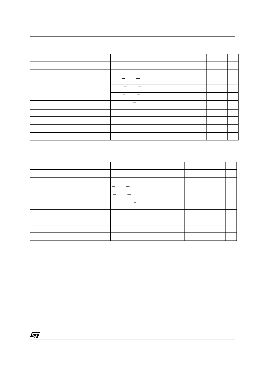
Figure 6. Software Chip Erase Algorithm
Wait for write completion (tQ5HQ5X)
AI02236C
Write AAh in
Address 5555h
Write 55h in
Address 2AAAh
Write 80h in
Address 5555h
Whole Array has been Set to FFh
Write AAh in
Address 5555h
Write 55h in
Address 2AAAh
Write 10h in
Address 5555h
Page Write
Timing
Time Out (tWLQ5H)
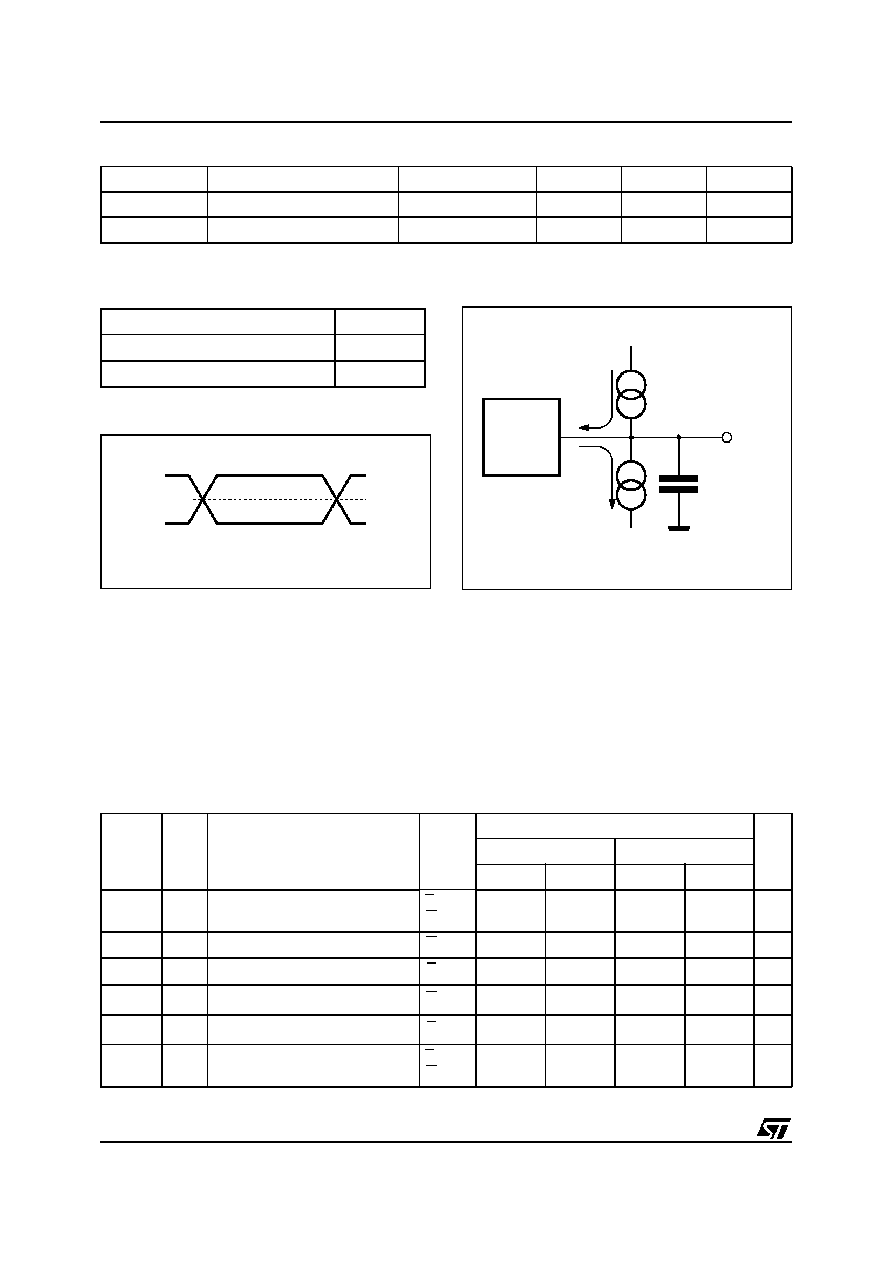
Figure 7. Status Bit Assignment
Figure 8. Software Data Protection Status Read
Algorithm
AI02486B
DP
TB
PLTS
X
X
X
PWA
SDP
DP
TB
PLTS
X
PWA
SDP
DQ7
DQ6
DQ5
DQ4
DQ3
DQ2
DQ1
DQ0
= Data Polling
= Toggle Bit
= Page Load Timer Status
= undefined
= Page Write Abort
= Software Data Protection
AI02237B
Write AAh in
Address 5555h
Write 55h in
Address 2AAAh
Write 20h in
Address 5555h
Normal User Mode
Read SDP
on DQ0
Write xxh in
Address xxxxh
Page Write
Timing

M28010
8/23
Software Chip Erase
The device can be erased (with all bytes set to
FFh) by using a six-byte software command code.
This operation can be initiated only if the user
loads, with a Page Write addressing mode, six
specific data bytes to six specific locations (as
shown in Figure 6). The complexity of the
sequence has been designed to guard against
inadvertent use of the command.
Status Bits
The devices provide five status bits (DQ7, DQ6,
DQ5, DQ1 and DQ0) for use during write
operations. These allow the application to use the
write time latency of the device for getting on with
other work. These signals are available on the I/O
port bits DQ7, DQ6, DQ5, DQ1 and DQ0 (but only
during the internal write cycle, t
Q5HQ5X
).
Data Polling bit (DQ7). The internally timed write
cycle starts as soon as t
WLQ5H
(defined in Table
9A to Table 9C) has elapsed since the previous
byte was latched in to the memory. The value of
the DQ7 bit of this last byte, is used as a signal
throughout this write operation: it is inverted while
the internal write operation is underway, and is
inverted back to its original value once the
operation is complete.
Toggle bit (DQ6). The device offers another way
for determining when the internal write cycle is
running. During the internal write cycle, DQ6
toggles from '0' to '1' and '1' to '0' (the first read
value being '0') on subsequent attempts to read
any byte of the memory. When the internal write
cycle is complete, the toggling is stopped, and the
values read on DQ7-DQ0 are those of the
addressed memory byte. This indicates that the
device is again available for new Read and Write
operations.
Page Load Timer Status bit (DQ5). An internal
timer is used to measure the period between
successive
Write operations,
up
to
t
WLQ5H
(defined in Table 9A to Table 9C). The DQ5 line is
held low to show when this timer is running (hence
showing that the device has received one write
operation, and is waiting for the next). The DQ5
line is held high when the counter has overflowed
(hence showing that the device is now starting the
internal write to the memory array).
Page Write Abort bit (DQ1). During a page write
operation, the A16 to A7 signals should be kept
constant.
They
should
not
change
while
successive data bytes are being transferred to the
internal latches of the memory device. If a change
occurs on any of the pins, A16 to A7, during the
page write operation (that is, before the falling
edge of W or E, which ever occurs later), the
internal write cycle is not started, and the internal
circuitry is completely reset.
The abort signal can be observed on the DQ1 pin,
using a normal read operation. This can be
performed at any time during the byte load cycle,
t
WLQ5H
, or while the W input is being held high
between two load cycles. The default value of DQ1
is initially set to '0' and changes to '1' if the internal
circuitry has detected a change on any of the
address pins A16 to A7. This PWA bit can be
checked regardless of whether Software Data
Protection is enabled or disabled.
Table 5A. Read Mode DC Characteristics for M28010 (5V range)
(T
A
= ≠40 to 85
∞
C; V
CC
= 4.5 to 5.5 V)
Note: 1. All inputs and outputs open circuit.
Symbol
Parameter
Test Condition
Min.
Max.
Unit
I
LI
Input Leakage Current
0 V
V
IN
V
CC
5
µ
A
I
LO
Output Leakage Current
0 V
V
OUT
V
CC
5
µ
A
I
CC
1
Supply Current (CMOS inputs)
E = V
IL
, G = V
IL
, f = 0.1 MHz
2
mA
E = V
IL
, G = V
IL
, f = 5 MHz
22
mA
E = V
IL
, G = V
IL
, f = 10 MHz
40
mA
I
CC1
1
Supply Current (Stand-by) CMOS
E > V
CC
≠ 0.3 V
50
µ
A
V
IL
Input Low Voltage
≠0.3
0.8
V
V
IH
Input High Voltage
2
V
CC
+ 0.3
V
V
OL
Output Low Voltage
I
OL
= 2.1 mA
0.4
V
V
OH
Output High Voltage
I
OH
= ≠400
µ
A
2.4
V
9/23
M28010
Table 5B. Read Mode DC Characteristics for M28010-W (3V range)
(T
A
= ≠40 to 85
∞
C; V
CC
= 2.7 to 3.6 V)
Note: 1. All inputs and outputs open circuit.
Table 5C. Read Mode DC Characteristics for M28010-R (2V range)
(T
A
= ≠40 to 85
∞
C; V
CC
= 1.8 to 2.4 V)
Note: 1. All inputs and outputs open circuit.
Symbol
Parameter
Test Condition
Min.
Max.
Unit
I
LI
Input Leakage Current
0 V
V
IN
V
CC
5
µ
A
I
LO
Output Leakage Current
0 V
V
OUT
V
CC
5
µ
A
I
CC
1
Supply Current (CMOS inputs)
E = V
IL
, G = V
IL
, f = 0.1 MHz
2
mA
E = V
IL
, G = V
IL
, f = 5 MHz
15
mA
E = V
IL
, G = V
IL
, f = 10 MHz
26
mA
I
CC1
1
Supply Current (Stand-by) CMOS
E > V
CC
≠ 0.3 V
30
µ
A
V
IL
Input Low Voltage
≠0.3
0.6
V
V
IH
Input High Voltage
2
V
CC
+ 0.3
V
V
OL
Output Low Voltage
I
OL
= 1.6 mA
0.45
V
V
OH
Output High Voltage
I
OH
= ≠100
µ
A
2.4
V
Symbol
Parameter
Test Conditio n
Min.
Max.
Unit
I
LI
Input Leakage Current
0 V
V
IN
V
CC
5
µ
A
I
LO
Output Leakage Current
0 V
V
OUT
V
CC
5
µ
A
I
CC
1
Supply Current (CMOS inputs)
E = V
IL
, G = V
IL
, f = 0.1 MHz, V
CC
= 2.4 V
2
mA
E = V
IL
, G = V
IL
, f = 5 MHz, V
CC
= 2.4 V
12
mA
I
CC1
1
Supply Current (Stand-by) CMOS
E > V
CC
≠ 0.3 V
30
µ
A
V
IL
Input Low Voltage
≠0.3
0.2
V
V
IH
Input High Voltage
V
CC
≠0.3
V
CC
+0.3
V
V
OL
Output Low Voltage
I
OL
= 0.4 mA
0.15
V
V
OH
Output High Voltage
I
OH
= ≠100
µ
A
V
CC
≠0.15
V
Software Data Protection bit (DQ0). Reading the
SDP bit (DQ0) allows the user to determine
whether the Software Data Protection mode has
been enabled (SDP=1) or disabled (SDP=0). The
SDP bit (DQ0) can be read by using a dedicated
algorithm (as shown in Figure 8), or can be
combined with the reading of the DP bit (DQ7), TB
bit (DQ6) and PLTS bit (DQ5).
M28010
10/23
Table 6. Input and Output Parameters
1
(T
A
= 25
∞
C, f = 1 MHz)
Note: 1. Sampled only, not 100% tested.
Symbol
Parameter
Test Condition
Min.
Max.
Unit
C
IN
Input Capacitance
V
IN
= 0 V
6
pF
C
OUT
Output Capacitance
V
OUT
= 0 V
12
pF
Table 7. AC Measurement Conditions
Input Rise and Fall Times
5 ns
Input Pulse Voltages
0 V to V
CC
Input and Output Timing Ref. Voltages
V
CC
/2
Figure 9. AC Testing Input Output Waveforms
AI02228
VCC
0V
VCC/2
Figure 10. AC Testing Equivalent Load Circuit
AI02578
OUT
CL = 30pF
CL includes JIG capacitance
IOL
DEVICE
UNDER
TEST
IOH
Table 8A. Read Mode AC Characteristics for M28010 (5V range)
(T
A
= ≠40 to 85
∞
C; V
CC
= 4.5 to 5.5 V)
Note: 1. Output Hi-Z is defined as the point at which data is no longer driven.
Symbol
Alt.
Parameter
Test
Condi t
ion
M28010
Unit
≠10
≠12
Min
Max
Min
Max
t
AVQV
t
ACC
Address Valid to Output Valid
E = V
IL
,
G = V
IL
100
120
ns
t
ELQV
t
CE
Chip Enable Low to Output Valid
G = V
IL
100
120
ns
t
GLQV
t
OE
Output Enable Low to Output Valid
E = V
IL
40
45
ns
t
EHQZ
1
t
DF
Chip Enable High to Output Hi-Z
G = V
IL
0
40
0
45
ns
t
GHQZ
1
t
DF
Output Enable High to Output Hi-Z
E = V
IL
0
40
0
45
ns
t
AXQX
t
OH
Address Transition to Output
Transition
E = V
IL
,
G = V
IL
0
0
ns
11/23
M28010
Table 8B. Read Mode AC Characteristics for M28010-W (3V range)
(T
A
= ≠40 to 85
∞
C; V
CC
= 2.7 to 3.6 V)
Note: 1. Output Hi-Z is defined as the point at which data is no longer driven.
Table 8C. Read Mode AC Characteristics for M28010-R (2V range)
(T
A
= ≠40 to 85
∞
C; V
CC
= 1.8 to 2.4 V)
Note: 1. Output Hi-Z is defined as the point at which data is no longer driven.
Symbol
Alt.
Parameter
Test
Condi t
ion
M28010-W
Unit
≠10
≠12
≠15
Min
Max
Min
Max
Min
Max
t
AVQV
t
ACC
Address Valid to Output Valid
E = V
IL
,
G = V
IL
100
120
150
ns
t
ELQV
t
CE
Chip Enable Low to Output Valid
G = V
IL
100
120
150
ns
t
GLQV
t
OE
Output Enable Low to Output Valid
E = V
IL
70
80
100
ns
t
EHQZ
1
t
DF
Chip Enable High to Output Hi-Z
G = V
IL
0
50
0
60
0
70
ns
t
GHQZ
1
t
DF
Output Enable High to Output Hi-Z
E = V
IL
0
50
0
60
0
70
ns
t
AXQX
t
OH
Address Transition to Output
Transition
E = V
IL
,
G = V
IL
0
0
0
ns
Symbol
Alt.
Parameter
Test
Condi t
ion
M28010-R
Unit
≠20
≠25
Min
Max
Min
Max
t
AVQV
t
ACC
Address Valid to Output Valid
E = V
IL
,
G = V
IL
200
250
ns
t
ELQV
t
CE
Chip Enable Low to Output Valid
G = V
IL
200
250
ns
t
GLQV
t
OE
Output Enable Low to Output Valid
E = V
IL
80
90
ns
t
EHQZ
1
t
DF
Chip Enable High to Output Hi-Z
G = V
IL
0
50
0
60
ns
t
GHQZ
1
t
DF
Output Enable High to Output Hi-Z
E = V
IL
0
50
0
60
ns
t
AXQX
t
OH
Address Transition to Output
Transition
E = V
IL
,
G = V
IL
0
0
ns

M28010
12/23
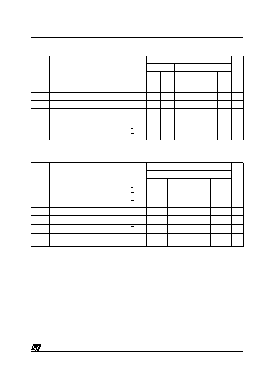
Table 9A. Write Mode AC Characteristics for M28010 (5V range)
(T
A
= ≠40 to 85
∞
C; V
CC
= 4.5 to 5.5 V)
Symbol
Alt.
Parameter
Test Condit ion
M28010
Unit
Min
Max
t
AVWL
t
AS
Address Valid to Write Enable Low
E = V
IL
, G = V
IH
0
ns
t
AVEL
t
AS
Address Valid to Chip Enable Low
G = V
IH
, W= V
IL
0
ns
t
ELWL
t
CES
Chip Enable Low to Write Enable Low
G = V
IH
0
ns
t
GHWL
t
OES
Output Enable High to Write Enable Low
E = V
IL
0
ns
t
GHEL
t
OES
Output Enable High to Chip Enable Low
W = V
IL
0
ns
t
WLEL
t
WES
Write Enable Low to Chip Enable Low
G = V
IH
0
ns
t
WLAX
t
AH
Write Enable Low to Address Transition
70
ns
t
ELAX
t
AH
Chip Enable Low to Address Transition
70
ns
t
ELEH
t
WP
Chip Enable Low to Chip Enable High
100
ns
t
WHEH
t
CEH
Write Enable High to Chip Enable High
0
ns
t
WHGL
t
OEH
Write Enable High to Output Enable Low
0
ns
t
EHWH
t
WEH
Chip Enable High to Write Enable High
0
ns
t
WHDX
t
DH
Write Enable High to Input Transition
0
ns
t
EHDX
t
DH
Chip Enable High to Input Transition
0
ns
t
WHWL
t
WPH
Write Enable High to Write Enable Low
50
ns
t
WLWH
t
WP
Write Enable Low to Write Enable High
100
ns
t
WLQ5H
t
BLC
Time-out after the last byte write
150
µ
s
t
Q5HQ5X
t
WC
Byte Write Cycle time
5
ms
Page Write Cycle time (up to 128 bytes)
10
ms
t
DVWH
t
DS
Data Valid before Write Enable High
50
ns
t
DVEH
t
DS
Data Valid before Chip Enable High
50
ns
Figure 11. Read Mode AC Waveforms (with Write Enable, W, high)
Note: 1. Write Enable (W) = V
IH
AI02229
VALID
tAVQV
tAXQX
tGLQV
tEHQZ
tGHQZ
DATA OUT
A0-A16
E
G
DQ0-DQ7
tELQV
Hi-Z
13/23
M28010
Table 9B. Write Mode AC Characteristics for M28010-W (3V range)
(T
A
= ≠40 to 85
∞
C; V
CC
= 2.7 to 3.6 V)
Symbol
Alt.
Parameter
Test Condit ion
M28010-W
Unit
Min
Max
t
AVWL
t
AS
Address Valid to Write Enable Low
E = V
IL
, G = V
IH
0
ns
t
AVEL
t
AS
Address Valid to Chip Enable Low
G = V
IH
, W= V
IL
0
ns
t
ELWL
t
CES
Chip Enable Low to Write Enable Low
G = V
IH
0
ns
t
GHWL
t
OES
Output Enable High to Write Enable Low
E = V
IL
0
ns
t
GHEL
t
OES
Output Enable High to Chip Enable Low
W = V
IL
0
ns
t
WLEL
t
WES
Write Enable Low to Chip Enable Low
G = V
IH
0
ns
t
WLAX
t
AH
Write Enable Low to Address Transition
70
ns
t
ELAX
t
AH
Chip Enable Low to Address Transition
70
ns
t
ELEH
t
WP
Chip Enable Low to Chip Enable High
100
ns
t
WHEH
t
CEH
Write Enable High to Chip Enable High
0
ns
t
WHGL
t
OEH
Write Enable High to Output Enable Low
0
ns
t
EHWH
t
WEH
Chip Enable High to Write Enable High
0
ns
t
WHDX
t
DH
Write Enable High to Input Transition
0
ns
t
EHDX
t
DH
Chip Enable High to Input Transition
0
ns
t
WHWL
t
WPH
Write Enable High to Write Enable Low
50
ns
t
WLWH
t
WP
Write Enable Low to Write Enable High
100
ns
t
WLQ5H
t
BLC
Time-out after the last byte write
150
µ
s
t
Q5HQ5X
t
WC
Byte Write Cycle time
5
ms
Page Write Cycle time (up to 128 bytes)
10
ms
t
DVWH
t
DS
Data Valid before Write Enable High
80
ns
t
DVEH
t
DS
Data Valid before Chip Enable High
80
ns

M28010
14/23
Table 9C. Write Mode AC Characteristics for M28010-R (2V range)
(T
A
= ≠40 to 85
∞
C; V
CC
= 1.8 to 2.4 V)
Symbol
Alt.
Parameter
Test Condit ion
M28010-R
Unit
Min
Max
t
AVWL
t
AS
Address Valid to Write Enable Low
E = V
IL
, G = V
IH
0
ns
t
AVEL
t
AS
Address Valid to Chip Enable Low
G = V
IH
, W= V
IL
0
ns
t
ELWL
t
CES
Chip Enable Low to Write Enable Low
G = V
IH
0
ns
t
GHWL
t
OES
Output Enable High to Write Enable Low
E = V
IL
0
ns
t
GHEL
t
OES
Output Enable High to Chip Enable Low
W = V
IL
0
ns
t
WLEL
t
WES
Write Enable Low to Chip Enable Low
G = V
IH
0
ns
t
WLAX
t
AH
Write Enable Low to Address Transition
120
ns
t
ELAX
t
AH
Chip Enable Low to Address Transition
120
ns
t
ELEH
t
WP
Chip Enable Low to Chip Enable High
120
ns
t
WHEH
t
CEH
Write Enable High to Chip Enable High
0
ns
t
WHGL
t
OEH
Write Enable High to Output Enable Low
0
ns
t
EHWH
t
WEH
Chip Enable High to Write Enable High
0
ns
t
WHDX
t
DH
Write Enable High to Input Transition
0
ns
t
EHDX
t
DH
Chip Enable High to Input Transition
0
ns
t
WHWL
t
WPH
Write Enable High to Write Enable Low
100
ns
t
WLWH
t
WP
Write Enable Low to Write Enable High
120
ns
t
WLQ5H
t
BLC
Time-out after the last byte write
150
µ
s
t
WHRH
t
WC
Byte Write Cycle time
5
ms
Page Write Cycle time (up to 128 bytes)
10
ms
t
DVWH
t
DS
Data Valid before Write Enable High
120
ns
t
DVEH
t
DS
Data Valid before Chip Enable High
120
ns

15/23
M28010
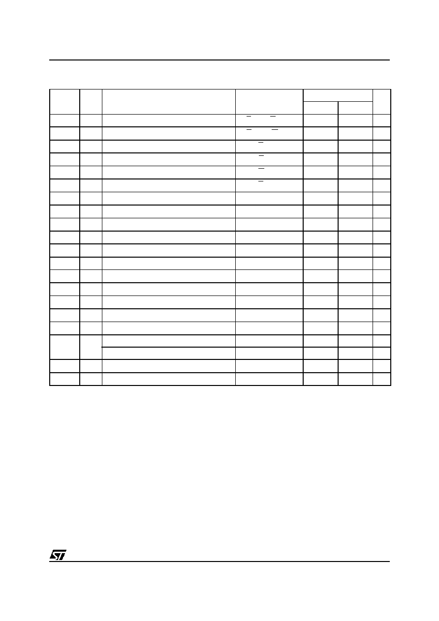
Figure 12. Write Mode AC Waveforms (Write Enable, W, controlled)
Figure 13. Write Mode AC Waveforms (Chip Enable, E, controlled)
AI02230
VALID
tAVWL
A0-A16
E
G
DQ0-DQ7
DATA IN
W
tWLAX
tELWL
tGHWL
tWHEH
tWHGL
tWLWH
tWHWL
tWHDX
tDVWH
AI02231
VALID
tAVEL
A0-A16
E
G
DQ0-DQ7
DATA IN
W
tELAX
tGHEL
tWLEL
tEHGL
tEHDX
tDVEH
tELEH
tEHWH

M28010
16/23
Figure 14. Page Write Mode AC Waveforms (Write Enable, W, controlled)
Figure 15. Software Protected Write Cycle Waveforms
Note: 1. A16 to A7 must specify the same page address during each high-to-low transition of W (or E). G must be high only when W and E
are both low.
tQ5HQ5X
AI02829B
A0-A16
E
G
DQ0-DQ7 (in)
W
Addr 0
DQ5 (out)
Addr 1
Addr 2
Addr n
tWLQ5H
tWLWH
tWHWL
Byte 0
Byte 1
Byte 2
Byte n
AI02233B
A7-A16
E
G
DQ0-DQ7
W
Page Add
1
tWLWH
tWHWL
AAh
55h
A0h
A0-A6
5555h
2AAAh
5555h
Byte Add n
tDVWH
tWHDX
Byte Add 0
Byte n
Byte 0
17/23
M28010
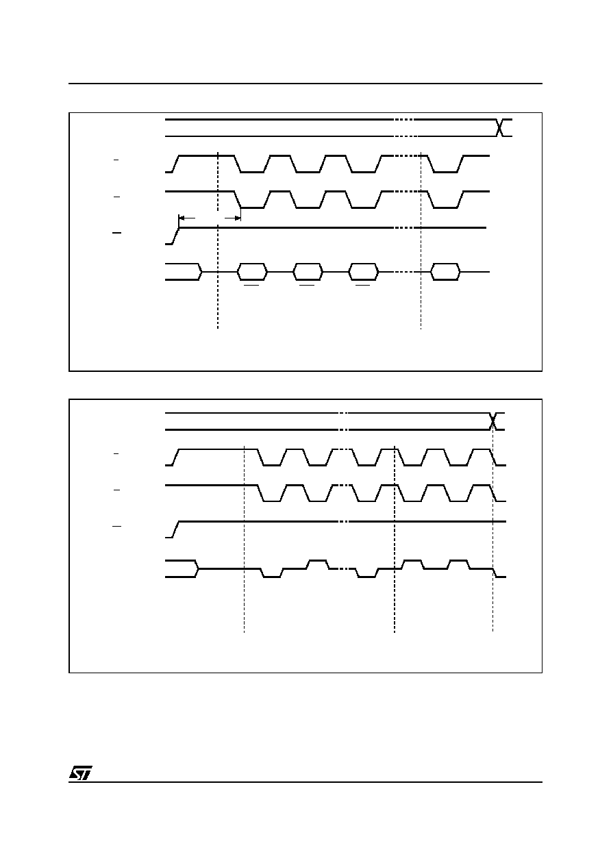
Figure 16. Data Polling Sequence Waveforms
Figure 17. Toggle Bit Sequence Waveforms
Note: 1. The Toggle Bit is first set to `0'.
AI02234
A0-A16
E
G
DQ7
W
DQ7
DQ7
DQ7
DQ7
DQ7
READY
AFTER INTERNAL
WRITE SEQUENCE
LAST BYTE
LOADED
INTERNAL WRITE SEQUENCE
OR
TIME BETWEEN TWO CONSECUTIVE
BYTES LOADING
Address of the last byte of the Page Write instruction
tWHGL
AI02235
A0-A16
E
G
DQ6
W
(1)
TOGGLE
READY
AFTER INTERNAL
WRITE SEQUENCE
LAST BYTE
LOADED
INTERNAL WRITE SEQUENCE
OR
TIME BETWEEN TWO CONSECUTIVE
BYTES LOADING
Address of the last byte of the Page Write instruction
M28010
18/23
Table 10. Ordering Information Scheme
Note: 1. This temperature range on request only.
Example:
M28010
≠
10
W
KA
6
T
Option
T
Tape & Reel Packing
Speed
-10
100 ns
Temperature Range
-12
120 ns
1
1
0 to 70
∞
C
-15
150 ns
6
≠40 to 85
∞
C
-20
200 ns
-25
250 ns
Operating Voltage
Package
blank 4.5 V to 5.5 V
BA
PDIP32
W
2.7 V to 3.6 V
KA
PLCC32
R
1.8 V to 2.4 V
NA
TSOP32: 8 x 20mm
ORDERING INFORMATION
Devices are shipped from the factory with the
memory content set at all `1's (FFh).
The notation used for the device number is as
shown in Table 10. For a list of available options
(speed, package, etc.) or for further information on
any aspect of this device, please contact the ST
Sales Office nearest to you.
19/23
M28010
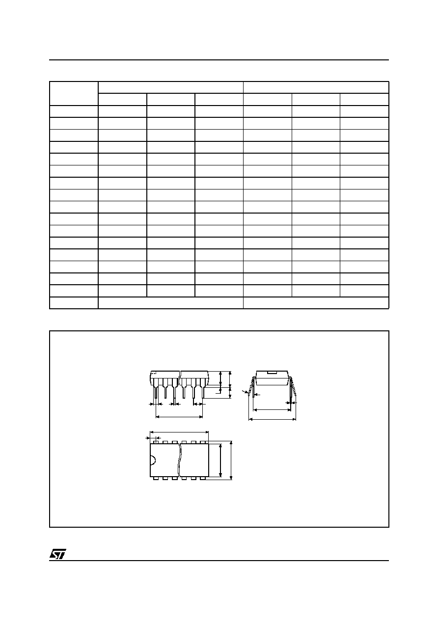
Figure 18. PDIP32 (BA)
Note:
1. Drawing is not to scale.
PDIP
A2
A1
A
L
B1
B
e1
D
S
E1
E
N
1
C
eA
eB
D2
Table 11. PDIP32 - 32 lead Plastic DIP, 600 mils width, Package Mechanical Data
Symbol
mm
inches
Typ.
Min.
Max.
Typ.
Min.
Max.
A
≠
5.08
≠
0.200
A1
0.38
≠
0.015
≠
A2
3.56
4.06
0.140
0.160
B
0.38
0.51
0.015
0.020
B1
1.52
≠
≠
0.060
≠
≠
C
0.20
0.30
0.008
0.012
D
41.78
42.04
1.645
1.655
D2
38.10
≠
≠
1.500
≠
≠
E
15.24
≠
≠
0.600
≠
≠
E1
13.59
13.84
0.535
0.545
e1
2.54
≠
≠
0.100
≠
≠
eA
15.24
≠
≠
0.600
≠
≠
eB
15.24
17.78
0.600
0.700
L
3.18
3.43
0.125
0.135
S
1.78
2.03
0.070
0.080
0
∞
10
∞
0
∞
10
∞
N
32
32

M28010
20/23
Table 12. PLCC32 - 32 lead Plastic Leaded Chip Carrier, rectangular
Symbol
mm
inches
Typ.
Min.
Max.
Typ.
Min.
Max.
A
2.54
3.56
0.100
0.140
A1
1.52
2.41
0.060
0.095
A2
≠
0.38
≠
0.015
B
0.33
0.53
0.013
0.021
B1
0.66
0.81
0.026
0.032
D
12.32
12.57
0.485
0.495
D1
11.35
11.56
0.447
0.455
D2
9.91
10.92
0.390
0.430
E
14.86
15.11
0.585
0.595
E1
13.89
14.10
0.547
0.555
E2
12.45
13.46
0.490
0.530
e
1.27
≠
≠
0.050
≠
≠
F
0.00
0.25
0.000
0.010
R
0.89
≠
≠
0.035
≠
≠
N
32
32
Nd
7
7
Ne
9
9
CP
0.10
0.004
Figure 19. PLCC32 (KA)
Note:
1. Drawing is not to scale.
PLCC
D
Ne
E1 E
1 N
D1
Nd
CP
B
D2/E2
e
B1
A1
A
R
0.51 (.020)
1.14 (.045)
F
A2

21/23
M28010
Table 13. TSOP32 - 32 lead Plastic Thin Small Outline, 8 x 20mm, Package Mechanical Data
Symbol
mm
inches
Typ.
Min.
Max.
Typ.
Min.
Max.
A
1.20
0.047
A1
0.05
0.17
0.002
0.006
A2
0.95
1.05
0.037
0.041
B
0.15
0.27
0.006
0.011
C
0.10
0.21
0.004
0.008
D
19.80
20.20
0.780
0.795
D1
18.30
18.50
0.720
0.728
E
7.90
8.10
0.311
0.319
e
0.50
≠
≠
0.020
≠
≠
L
0.50
0.70
0.020
0.028
0
∞
5
∞
0
∞
5
∞
N
32
32
CP
0.10
0.004
Figure 20. TSOP32 (NS)
Note:
1. Drawing is not to scale.
TSOP-a
D1
E
1
N
CP
B
e
A2
A
N/2
D
DIE
C
L
A1

M28010
22/23
Table 14. Revision History
Date
Description of Revision
15-Feb-2000
I
CC1
(max), in Read Mode DC Char table for 5V, changed from 30
µ
A to 50
µ
A.
28-Feb-2000
t
DVWH
(min) and t
DVEH
(min), in Write Mode AC Char table for 3V, changed from 50 ns to 80 ns

23/23
M28010
Information furnished is believed to be accurate and reliable. However, STMi croelectronics assumes no responsibility for the consequences
of use of such information nor for any infringement of patents or other rights of third parties which may result from its use. No license is granted
by implication or otherwise under any patent or patent rights of STMicroelectronics. Specifications mentioned in this publication are subject
to change without notice. This publication supersedes and replaces all information previously supplied. STMicroelectronics products are not
authorized for use as criti cal components in life support devices or systems without express writt en approval of STMicroelectronics.
©
2000 STMicroelectronics - All Rights Reserved
The ST logo is a registered trademark of STMicroelectronics.
All other names are the property of their respective owners.
STMicroelectronics GROUP OF COMPANIES
Australia - Brazil - China - France - Germany - Italy - Japan - Korea - Malaysia - Malta - Mexico - Morocco - The Netherlands - Singapore -
Spain - Sweden - Switzerland - Taiwan - Thailand - United Kingdom - U.S.A.
http:// www.st.com