M28256
256 Kbit (32Kb x8) Parallel EEPROM
with Software Data Protection
PRELIMINARY DATA
January 1999
1/21
This is preliminary information on a new product now in developmentor undergoing evaluation . Detail s are subject to change without notice.
AI01885
15
A0-A14
W
DQ0-DQ7
VCC
M28256
G
E
VSS
8
Figure 1. Logic Diagram
28
1
PDIP28 (BS)
PLCC32 (KA)
A0-A14
Address Input
DQ0-DQ7
Data Input / Output
W
Write Enable
E
Chip Enable
G
Output Enable
V
CC
Supply Voltage
V
SS
Ground
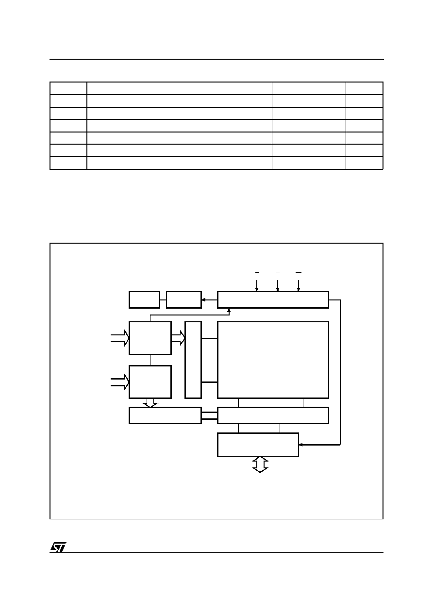
Table 1. Signal Names
FAST ACCESS TIME:
≠ 90ns at 5V
≠ 120ns at 3V
SINGLE SUPPLY VOLTAGE:
≠ 5V
±
10% for M28256
≠ 2.7V to 3.6V for M28256-xxW
LOW POWER CONSUMPTION
FAST WRITE CYCLE:
≠ 64 Bytes Page Write Operation
≠ Byte or Page Write Cycle
ENHANCED END of WRITE DETECTION:
≠ Data Polling
≠ Toggle Bit
STATUS REGISTER
HIGH RELIABILITY DOUBLE POLYSILICON,
CMOS TECHNOLOGY:
≠ Endurance >100,000 Erase/Write Cycles
≠ Data Retention >10 Years
JEDEC APPROVED BYTEWIDE PIN OUT
ADDRESS and DATA LATCHED ON-CHIP
SOFTWARE DATA PROTECTION
DESCRIPTION
The M28256 and M28256-Ware 32K x8 low power
Parallel EEPROM fabricatedwith STMicroelectron-
ics proprietary double polysilicon CMOS technol-
ogy.
TSOP28 (NS)
8 x13.4mm
28
1
SO28 (MS)
300 mils

A1
A0
DQ0
A7
A4
A3
A2
A6
A5
A13
A10
A8
A9
DQ7
W
A11
G
E
DQ5
DQ1
DQ2
DQ3
VSS
DQ4
DQ6
A12
A14
VCC
AI01886
M28256
8
1
2
3
4
5
6
7
9
10
11
12
13
14
16
15
28
27
26
25
24
23
22
21
20
19
18
17
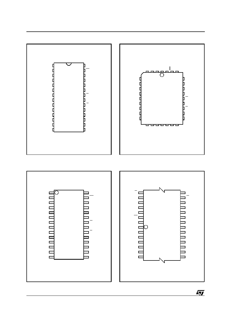
Figure 2A. DIP Pin Connections
AI01887
A13
A8
A10
DQ4
17
A0
NC
DQ0
DQ1
DQ2
DU
DQ3
A6
A3
A2
A1
A5
A4
9
W
A9
1
A14
A11
DQ6
A7
DQ7
32
DU
V
CC
M28256
A12
NC
DQ5
G
E
25
V
SS
Figure 2B. LCC Pin Connections
Warning: NC = Not Connected, DU = Don't Use.
A1
A0
DQ0
A5
A2
A4
A3
A9
A11
DQ7
A8
G
E
DQ5
DQ1
DQ2
DQ3
DQ4
DQ6
A13
W
A12
A6
A14
VCC
A7
AI01889
M28256
28
1
22
7
8
14
15
21
VSS
A10
Figure 2D. TSOP Pin Connections
DQ0
DQ1
A3
A0
A2
A1
A10
E
A13
DQ7
G
DQ5
VCC
DQ4
A9
W
A4
A14
A7
AI01888
M28256
8
2
3
4
5
6
7
9
10
11
12
13
14
22
21
20
19
18
17
16
15
DQ2
VSS
A6
A5
DQ6
28
27
26
25
24
23
A11
DQ3
1
A12
A8
Figure 2C. SO Pin Connections
2/21
M28256

Symbol
Parameter
Value
Unit
T
A
Ambient Operating Temperature
(2)
≠ 40 to 85
∞
C
T
STG
Storage Temperature Range
≠ 65 to 150
∞
C
V
CC
Supply Voltage
≠ 0.3 to 6.5
V
V
IO
Input/Output Voltage
≠ 0.3 to V
CC
+0.6
V
V
I
Input Voltage
≠ 0.3 to 6.5
V
V
ESD
Electrostatic Discharge Voltage (Human Body model)
(3)
4000
V
Notes: 1. Except for the rating "Operating Temperature Range", stresses above those listed in the Table "Absolute Maximum Ratings" may
cause permanent damage to the device. These are stress ratings only and operation of the device at these or any other conditions
above those indicated in the Operating sections of this specification is not implied. Exposure to Absolute Maximum Rating
conditions for extended periods may affect device reliability. Refer also to the STMicroelectronics SURE Program and other
relevant quality documents.
2. Depends on range.
3. 100pF through 1500
; MIL-STD-883C, 3015.7
Table 2. Absolute Maximum Ratings
(1)
AI01697
ADDRESS
LATCH
A6-A14
(Page Address)
X
DECODE
CONTROL LOGIC
256K ARRAY
ADDRESS
LATCH
A0-A5
Y DECODE
VPP GEN
RESET
SENSE AND DATA LATCH
I/O BUFFERS
E
G
W
PAGE LOAD
TIMER STATUS
TOGGLE BIT
DATA POLLING
DQ0-DQ7
Figure 3. Block Diagram
3/21
M28256

Mode
E
G
W
DQ0 - DQ7
Read
V
IL
V
IL
V
IH
Data Out
Write
V
IL
V
IH
V
IL
Data In
Standby / Write Inhibit
V
IH
X
X
Hi-Z
Write Inhibit
X
X
V
IH
Data Out or Hi-Z
Write Inhibit
X
V
IL
X
Data Out or Hi-Z
Output Disable
X
V
IH
X
Hi-Z
Notes: 1. X = V
IH
or V
IL.
Table 3. Operating Modes
(1)
The devices offer fast access time with low power
dissipation and requires a 5V or 3V power supply.
The circuit has been designed to offer a flexible
microcontroller interface featuring both hardware
and software handshaking with Data Polling and
Toggle Bit and access to a status register. The
devices support a 64 byte page write operation. A
Software Data Protection (SDP) is also possible
using the standard JEDEC algorithm.
PIN DESCRIPTION
Addresses (A0-A14). The address inputs select
an 8-bit memory location during a read or write
operation.
Chip Enable (E). The chip enable input must be
low to enable all read/write operations. When Chip
Enable is high, power consumption is reduced.
Output Enable (G). The Output Enable input con-
trols the data output buffers and is used to initiate
read operations.
Data In/ Out (DQ0- DQ7). Data is written to or read
from the memory through the I/O pins.
Write Enable (W). The Write Enable input controls
the writing of data to the memory.
OPERATIONS
Write Protection
In order to prevent data corruption and inadvertent
write operations; an internal V
CC
comparator inhib-
its Write operations if V
CC
is below VWI (see Table
7 andTable 9).Access to the memory in write mode
is allowed after a power-up as specified in Table 7
and Table 9.
Read
The device is accessed like a static RAM. When E
and G are low with W high, the data addressed is
presented on the I/O pins. The I/O pins are high
impedance when either G or E is high.
Write
Write operations are initiated when both W and E
are low and G is high.The device supports both E
and W controlled write cycles. The Address is
latched by the falling edge of E or W which ever
occurs last and the Data on the rising edge of E or
W which ever occurs first. Once initiated the write
operation is internally timed until completion and
the status of the Data Polling and the Toggle Bit
functions on DQ7 and DQ6 is controlled accord-
ingly.
Page Write
Page write allows up to 64 bytes within the same
page to be consecutively latched into the memory
prior to initiating a programming cycle. All bytes
must be located in a single page address, that is
A14-A6 must be the same for all bytes; if not, the
Page Write instruction is not executed. The page
write can be initiated by any byte write operation.
A page write is composed of successive Write
instructions which have to be sequenced with a
specific period of time between two consecutive
Write instructions, period of time which has to be
smaller than the t
WHWH
value (see Table 12 and
Table 13).
If this period of time exceeds the t
WHWH
value, the
internal programmingcycle will start. Once initiated
the write operation is internally timed until comple-
tion and the status of the Data Polling and the
Toggle Bit functions on DQ7 and DQ6 is controlled
accordingly.
DESCRIPTION (Cont'd)
4/21
M28256

Status Register
The devices provide several Write operation status
flags that can be used to minimize the application
write time. These signals are available on the I/O
port bits during programming cycle only.
Data Polling bit (DQ7). During the internal write
cycle, any attempt to read the last byte written will
produce on DQ7 the complementary value of the
previously latched bit. Once the write cycle is fin-
ished the true logic value appears on DQ7 in the
read cycle.
Toggle bit (DQ6). The devices offer another way
for determining when the internal write cycle is
completed. During the internal Erase/Write cycle,
DQ6 will toggle from "0" to "1" and "1" to "0" (the
first read value is "0") on subsequent attempts to
read any byte of the memory. When the internal
cycle is completed the toggling will stop and the
data read on DQ7-DQ0 is the addressed memory
byte. The device is now accessible for a new Read
or Write operation.
Page Load Timer Status bit (DQ5). Duringa Page
Write instruction, the devices expect to receive the
stream of data with a minimum period of time
between each data byte. This period of time
(t
WHWH
) is defined by the on-chip Page Load timer
which running/overflow status is available on DQ5.
DQ5 Low indicates that the timer is running, DQ5
High indicates the time-out after which the internal
write cycle will start.
Software Data Protection
The devices offer a software controlled write pro-
tection facility that allows the user to inhibit all write
modes to the device. This can be useful in protect-
ing the memory from inadvertent write cycles that
may occur due to uncontrolledbus conditions.
The devices are shipped as standardin the "unpro-
tected" state meaning that the memory contents
can be changed as required by the user. After the
Software Data Protection enable algorithm is is-
sued, the device
enters the "Protect Mode" of
operation where no further write commands have
any effect on the memory contents.
The devices remain in this
mode until a valid
Software Data Protection (SDP) disable sequence
is received whereby the device reverts to its "un-
protected" state. The Software Data Protection is
fully non-volatile and is not changed by power
on/off sequences. To enable the Software Data
Protection (SDP) the device requires the user to
write (with a Page Write addressing three specific
data bytes to three specific memory locations,each
location in a different page) as per Figure 6. Simi-
larly to disable the Software Data Protection the
user has to write specific data bytes into six differ-
ent locations as per Figure 5 (with a Page Write
adressing different bytes in different pages).
This complexseries ensures that the userwill never
enable or disable the Software Data Protection
accidentally.
To write into the devices when SDP is set, the
sequence shown in Figure 6 must be used. This
sequence provides an unlock key to enable the
write action, and at the same time SDP continues
to be set.
An extension to this is where SDP is required to be
set, and data is to be written.
Using the same sequence as above, the data can
be written and SDP is set at the same time, giving
both these actions in the same Write cycle (t
WC
).
DQ7
DQ6 DQ5 DQ4 DQ3 DQ2 DQ1 DQ0
DP
TB
PLTS
X
X
X
X
X
DP
= Data Polling
TB
= Toggle Bit
PLTS = Page Load Timer Status
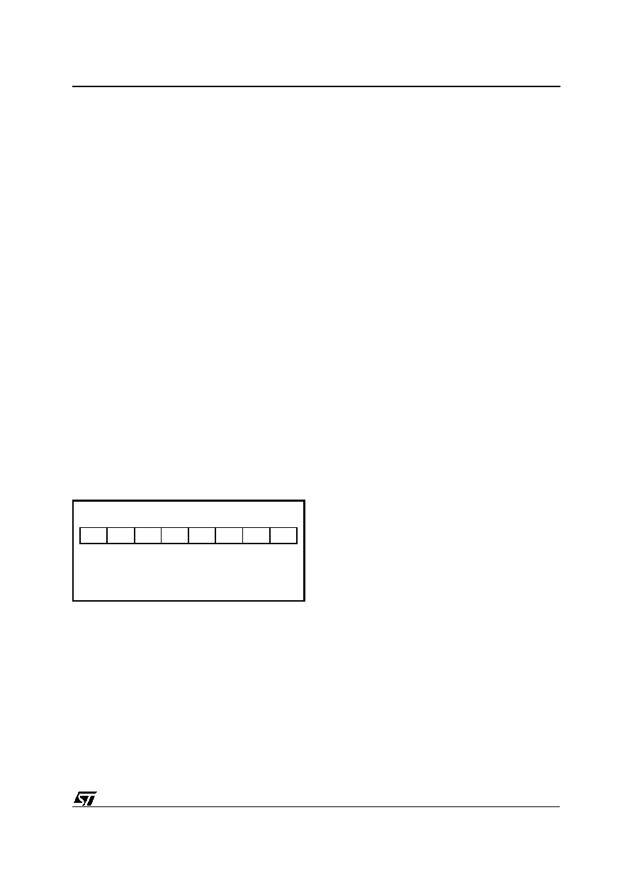
Figure 4. Status Bit Assignment
5/21
M28256

AI01698B
WRITE AAh in
Address 5555h
WRITE 55h in
Address 2AAAh
WRITE A0h in
Address 5555h
SDP is set
WRITE AAh in
Address 5555h
WRITE 55h in
Address 2AAAh
WRITE A0h in
Address 5555h
WRITE Data to
be Written in
any Address
SDP ENABLE ALGORITHM
Page
Write
Instruction
Page
Write
Instruction
WRITE
is enabled
SDP
Set
SDP
not Set
Write
in Memory
Write Data
+
SDP Set
after tWC
Figure 5. Software Data Protection Enable Algorithm and Memory Write
AI01699B
WRITE AAh in
Address 5555h
WRITE 55h in
Address 2AAAh
WRITE 80h in
Address 5555h
Unprotected State
after
tWC (Write Cycle time)
WRITE AAh in
Address 5555h
WRITE 55h in
Address 2AAAh
WRITE 20h in
Address 5555h
Page
Write
Instruction
Figure 6. Software Data Protection Disable Algorithm
6/21
M28256

Input Rise and Fall Times
20ns
Input Pulse Voltages (M28256)
0.4V to 2.4V
Input Pulse Voltages (M28256-W)
0V to V
CC
≠0.3V
Input and Output Timing Ref. Voltages (M28256)
0.8V to 2.0V
Input and Output Timing Ref. Voltages (M28256-W)
0.5 V
CC
Table 4. AC Measurement Conditions
AI02101B
4.5V to 5.5V Operating Voltage
2.7V to 3.6V Operating Voltage
VCC ≠ 0.3V
0V
0.5 VCC
2.4V
0.4V
2.0V
0.8V
Figure 7. AC Testing Input Output Waveforms
AI02102B
OUT
CL = 100pF
CL includes JIG capacitance
IOL
DEVICE
UNDER
TEST
IOH
Figure 8. AC Testing Equivalent Load Circuit
Symbol
Parameter
Test Condition
Min
Max
Unit
C
IN
Input Capacitance
V
IN
= 0V
6
pF
C
OUT
Output Capacitance
V
OUT
= 0V
12
pF
Note: 1. Sampled only, not 100% tested.
Table 5. Capacitance
(1)
(T
A
= 25
∞
C, f = 1 MHz )
Symbol
Parameter
Test Condition
Min
Max
Unit
I
LI
Input Leakage Current
0V
V
IN
V
CC
10
µ
A
I
LO
Output Leakage Current
0V
V
IN
V
CC
10
µ
A
I
CC
(1)
Supply Current (TTL inputs)
E = V
IL
, G = V
IL
, f = 5 MHz
30
mA
Supply Current (CMOS inputs)
E = V
IL
, G = V
IL
, f = 5 MHz
25
mA
I
CC1
(1)
Supply Current (Standby) TTL
E = V
IH
1
mA
I
CC2
(1)
Supply Current (Standby) CMOS
E > V
CC
≠0.3V
100
µ
A
V
IL
Input Low Voltage
≠ 0.3
0.8
V
V
IH
Input High Voltage
2
V
CC
+ 0.5
V
V
OL
Output Low Voltage
I
OL
= 2.1 mA
0.4
V
V
OH
Output High Voltage
I
OH
= ≠400
µ
A
2.4
Note: 1. All I/O's open circuit.
Table 6. Read Mode DC Characteristics for M28256
(T
A
= 0 to 70
∞
C or ≠40 to 85
∞
C; V
CC
= 4.5V to 5.5V)
7/21
M28256

Symbol
Parameter
Min
Max
Unit
t
PUR
Time Delay to Read Operation
1
µ
s
t
PUW
Time Delay to Write Operation (once V
CC
V
WI
)
5
ms
V
WI
Write Inhibit Threshold
3.0
4.2
V
Note: 1. Sampled only, not 100% tested.
Table 7. Power Up Timing for M28256
(1)
(T
A
= 0 to 70
∞
C or ≠40 to 85
∞
C; V
CC
= 4.5V to 5.5V)
Symbol
Parameter
Test Condition
Min
Max
Unit
I
LI
Input Leakage Current
0V
V
IN
V
CC
10
µ
A
I
LO
Output Leakage Current
0V
V
IN
V
CC
10
µ
A
I
CC
(1)
Supply Current (CMOS inputs)
E = V
IL
, G = V
IL
, f = 5 MHz, V
CC
= 3.3V
15
mA
E = V
IL
, G = V
IL
, f = 5 MHz, V
CC
= 3.6V
15
mA
I
CC2
(1)
Supply Current (Standby) CMOS
E > V
CC
≠0.3V
20
µ
A
V
IL
Input Low Voltage
≠ 0.3
0.6
V
V
IH
Input High Voltage
2
V
CC
+ 0.5
V
V
OL
Output Low Voltage
I
OL
= 2.1 mA
0.2 V
CC
V
V
OH
Output High Voltage
I
OH
= ≠400
µ
A
0.8 V
CC
V
Note: 1. All I/O's open circuit.
Table 8. Read Mode DC Characteristics for M28256-W
(T
A
= 0 to 70
∞
C or ≠40 to 85
∞
C; V
CC
= 2.7V to 3.6V)
Symbol
Parameter
Min
Max
Unit
t
PUR
Time Delay to Read Operation
1
µ
s
t
PUW
Time Delay to Write Operation (once V
CC
V
WI
)
10
ms
V
WI
Write Inhibit Threshold
1.5
2.5
V
Note: 1. Sampled only, not 100% tested.
Table 9. Power Up Timing for M28256-W
(1)
(T
A
= 0 to 70
∞
C or ≠40 to 85
∞
C; V
CC
= 2.7V to 3.6V)
8/21
M28256

Symbol
Alt
Parameter
Test Condition
M28256
Unit
-90
-12
-15
-20
min
max
min
max
min
max
min
max
t
AVQV
t
ACC
Address Valid to
Output Valid
E = V
IL
, G = V
IL
90
120
150
200
ns
t
ELQV
t
CE
Chip Enable Low to
Output Valid
G = V
IL
90
120
150
200
ns
t
GLQV
t
OE
Output Enable Low
to Output Valid
E = V
IL
40
45
50
50
ns
t
EHQZ
(1)
t
DF
Chip Enable High to
Output Hi-Z
G = V
IL
0
40
0
45
0
50
0
50
ns
t
GHQZ
(1)
t
DF
Output Enable High
to Output Hi-Z
E = V
IL
0
40
0
45
0
50
0
50
ns
t
AXQX
t
OH
Address Transition
to Output Transition
E = V
IL
, G = V
IL
0
0
0
0
ns
Note: 1. Output Hi-Z is defined as the point at which data is no longer driven.
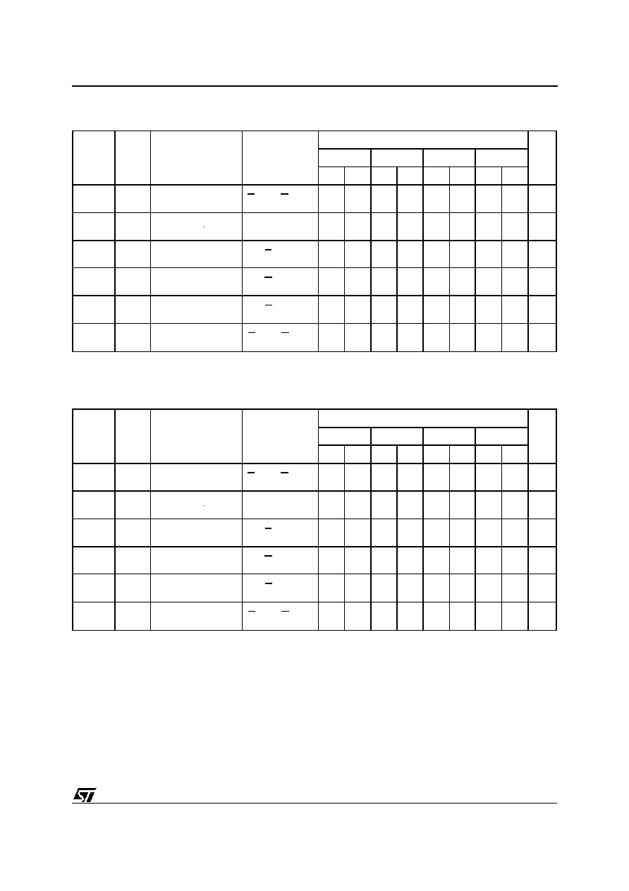
Table 10. Read Mode AC Characteristics
(T
A
= 0 to 70
∞
C or ≠40 to 85
∞
C; V
CC
= 4.5V to 5.5V)
Symbol
Alt
Parameter
Test Condition
M28256-W
Unit
-12
-15
-20
-25
min
max
min
max
min
max
min
max
t
AVQV
t
ACC
Address Valid to
Output Valid
E = V
IL
, G = V
IL
120
150
200
250
ns
t
ELQV
t
CE
Chip Enable Low to
Output Valid
G = V
IL
120
150
200
250
ns
t
GLQV
t
OE
Output Enable Low
to Output Valid
E = V
IL
45
70
80
100
ns
t
EHQZ
(1)
t
DF
Chip Enable High to
Output Hi-Z
G = V
IL
0
45
0
50
0
55
0
60
ns
t
GHQZ
(1)
t
DF
Output Enable High
to Output Hi-Z
E = V
IL
0
45
0
50
0
55
0
60
ns
t
AXQX
t
OH
Address Transition
to Output Transition
E = V
IL
, G = V
IL
0
0
0
0
ns
Note: 1. Output Hi-Z is defined as the point at which data is no longer driven.
Table 11. Read Mode AC Characteristics
(T
A
= 0 to 70
∞
C or ≠40 to 85
∞
C; V
CC
= 2.7V to 3.6V)
9/21
M28256

Symbol
Alt
Parameter
Test Condition
M28256
Unit
Min
Max
t
AVWL
t
AS
Address Valid to Write Enable Low
E = V
IL
, G = V
IH
0
ns
t
AVEL
t
AS
Address Valid to Chip Enable Low
G = V
IH
, W = V
IL
0
ns
t
ELWL
t
CES
Chip Enable Low to Write Enable Low
G = V
IH
0
ns
t
GHWL
t
OES
Output Enable High to Write Enable
Low
E = V
IL
0
ns
t
GHEL
t
OES
Output Enable High to Chip Enable Low
W = V
IL
0
ns
t
WLEL
t
WES
Write Enable Low to Chip Enable Low
G = V
IH
0
ns
t
WLAX
t
AH
Write Enable Low to Address Transition
50
ns
t
ELAX
t
AH
Chip Enable Low to Address Transition
50
ns
t
WLDV
t
DV
Write Enable Low to Input Valid
E = V
IL
, G = V
IH
1
µ
s
t
ELDV
t
DV
Chip Enable Low to Input Valid
G = V
IH
, W = V
IL
1
µ
s
t
ELEH
t
WP
Chip Enable Low to Chip Enable High
50
ns
t
WHEH
t
CEH
Write Enable High to Chip Enable High
0
ns
t
WHGL
t
OEH
Write Enable High to Output Enable
Low
0
ns
t
EHGL
t
OEH
Chip Enable High to Output Enable Low
0
ns
t
EHWH
t
WEH
Chip Enable High to Write Enable High
0
ns
t
WHDX
t
DH
Write Enable High to Input Transition
0
ns
t
EHDX
t
DH
Chip Enable High to Input Transition
0
ns
t
WHWL
t
WPH
Write Enable High to Write Enable Low
100
ns
t
WLWH
t
WP
Write Enable Low to Write Enable High
50
ns
t
WHWH
t
BLC
Byte Load Repeat Cycle Time
0.15
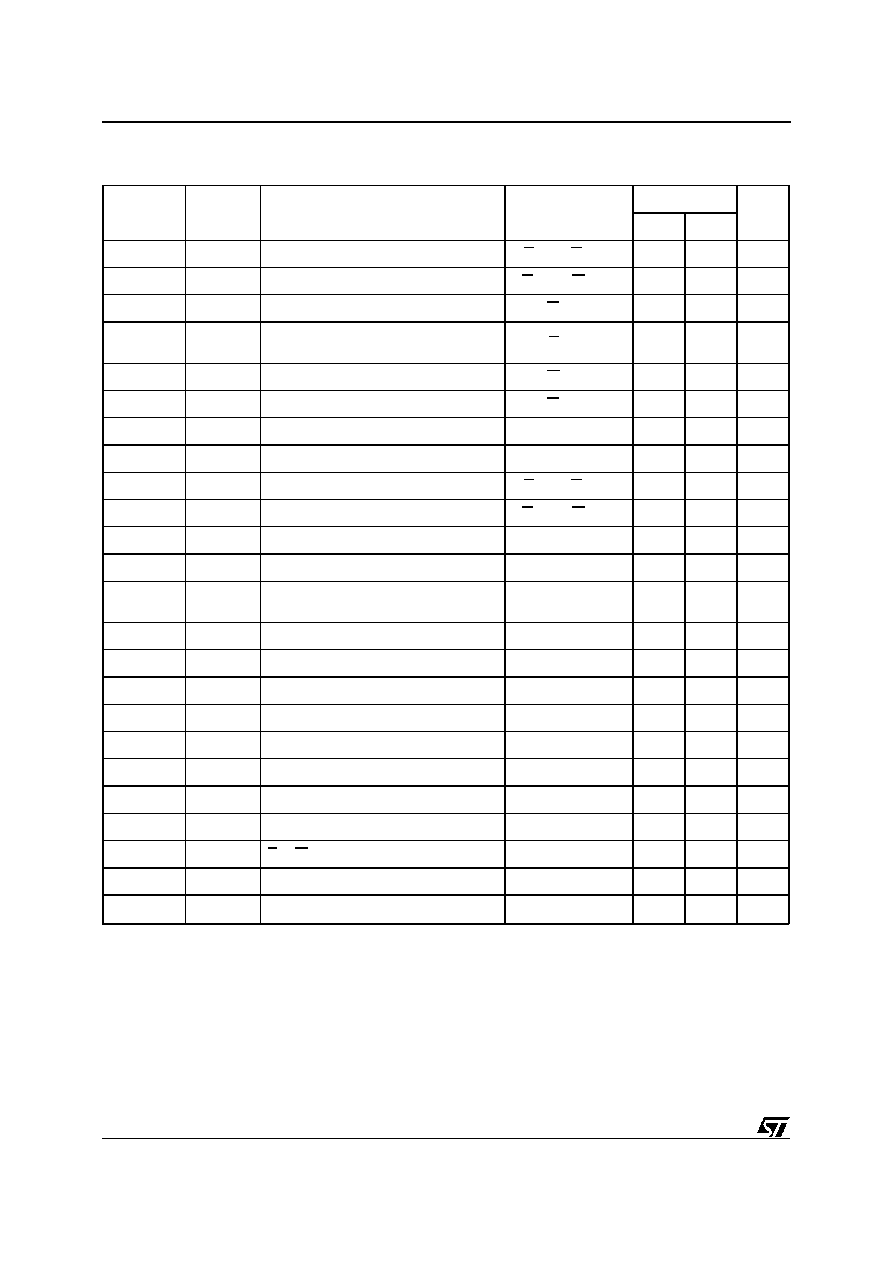
150
µ
s
t
WHRH
t
WC
Write Cycle Time
5
ms
t
EL
, t
WL
E or W Input Filter Pulse Width
Note 1
10
ns
t
DVWH
t
DS
Data Valid before Write Enable High
50
ns
t
DVEH
t
DS
Data Valid before Chip Enable High
50
ns
Note: 1. Characterized only but not tested in production.
Table 12. Write Mode AC Characteristics
(T
A
= 0 to 70
∞
C or ≠40 to 85
∞
C; V
CC
= 4.5V to 5.5V)
10/21
M28256

Symbol
Alt
Parameter
Test Condition
M28256-W
Unit
Min
Max
t
AVWL
t
AS
Address Valid to Write Enable Low
E = V
IL
, G = V
IH
0
ns
t
AVEL
t
AS
Address Valid to Chip Enable Low
G = V
IH
, W = V
IL
0
ns
t
ELWL
t
CES
Chip Enable Low to Write Enable Low
G = V
IH
0
ns
t
GHWL
t
OES
Output Enable High to Write Enable
Low
E = V
IL
0
ns
t
GHEL
t
OES
Output Enable High to Chip Enable Low
W = V
IL
0
ns
t
WLEL
t
WES
Write Enable Low to Chip Enable Low
G = V
IH
0
ns
t
WLAX
t
AH
Write Enable Low to Address Transition
70
ns
t
ELAX
t
AH
Chip Enable Low to Address Transition
70
ns
t
WLDV
t
DV
Write Enable Low to Input Valid
E = V
IL
, G = V
IH
1
µ
s
t
ELDV
t
DV
Chip Enable Low to Input Valid
G = V
IH
, W = V
IL
1
µ
s
t
ELEH
t
WP
Chip Enable Low to Chip Enable High
100
ns
t
WHEH
t
CEH
Write Enable High to Chip Enable High
0
ns
t
WHGL
t
OEH
Write Enable High to Output Enable
Low
0
ns
t
EHGL
t
OEH
Chip Enable High to Output Enable Low
0
ns
t
EHWH
t
WEH
Chip Enable High to Write Enable High
0
ns
t
WHDX
t
DH
Write Enable High to Input Transition
0
ns
t
EHDX
t
DH
Chip Enable High to Input Transition
0
ns
t
WHWL
t
WPH
Write Enable High to Write Enable Low
100
ns
t
WLWH
t
WP
Write Enable Low to Write Enable High
100
ns
t
WHWH
t
BLC
Byte Load Repeat Cycle Time
0.2
150
µ
s
t
WHRH
t
WC
Write Cycle Time
5
ms
t
EL
, t
WL
E or W Input Filter Pulse Width
Note 1
10
ns
t
DVWH
t
DS
Data Valid before Write Enable High
50
ns
t
DVEH
t
DS
Data Valid before Chip Enable High
50
ns
Note: 1. Characterized only but not tested in production.
Table 13. Write Mode AC Characteristics
(T
A
= 0 to 70
∞
C or ≠40 to 85
∞
C; V
CC
= 2.7V to 3.6V)
11/21
M28256

Note: Write Enable (W) = High.
AI01700
VALID
tAVQV
tAXQX
tGLQV
tEHQZ
tGHQZ
DATA OUT
A0-A14
E
G
DQ0-DQ7
tELQV
Hi-Z
Figure 9. Read Mode AC Waveforms
AI01701
VALID
tAVWL
A0-A14
E
G
DQ0-DQ7
DATA IN
W
tWLAX
tELWL
tGHWL
tWLDV
tWHEH
tWHGL
tWLWH
tWHWL
tWHDX
tDVWH
Figure 10. Write Mode AC Waveforms - Write Enable Controlled
12/21
M28256

AI01702
VALID
tAVEL
A0-A14
E
G
DQ0-DQ7
DATA IN
W
tELAX
tGHEL
tWLEL
tELDV
tEHGL
tEHDX
tDVEH
tELEH
tEHWH
Figure 11. Write Mode AC Waveforms - Chip Enable Controlled
AI01703B
A0-A14
E
G
DQ0-DQ7
W
tWHWH
Addr 0
DQ5
Addr 1
Addr 2
Addr n
tWHWH
tWHRH
tWLWH
tWHWL
Byte 0
Byte 1
Byte 2
Byte n
Byte n
Figure 12. Page Write Mode AC Waveforms - Write Enable Controlled
13/21
M28256

AI01704
A0-A5
E
G
DQ0-DQ7
W
tWLWH
tDVWH
Byte 0
tWHWL
A6-A14
tWLAX
tWHWH
tWHDX
tAVEL
5555h
2AAAh
5555h
Byte 62
Byte 63
AAh
55h
A0h
Byte Address
Page Address
Figure 13. Software Protected Write Cycle Waveforms
Note: A6 through A14 must specify the same page address during each high to low transition of W (or E) after the software code has been
entered. G must be high only when W and E are both low.
AI01705
A0-A14
E
G
DQ7
W
DQ7
DQ7
DQ7
DQ7
DQ7
READY
LAST WRITE
INTERNAL WRITE SEQUENCE
Address of the last byte of the Page Write instruction
Figure 14. Data Polling Waveform Sequence
14/21
M28256

AI01706
A0-A14
E
G
DQ6
W
READY
LAST WRITE
INTERNAL WRITE SEQUENCE
(1)
TOGGLE
DQ6
DQ6
Figure 15. Toggle Bit Waveform Sequence
Note: 1. First Toggle bit is forced to '0'.
15/21
M28256

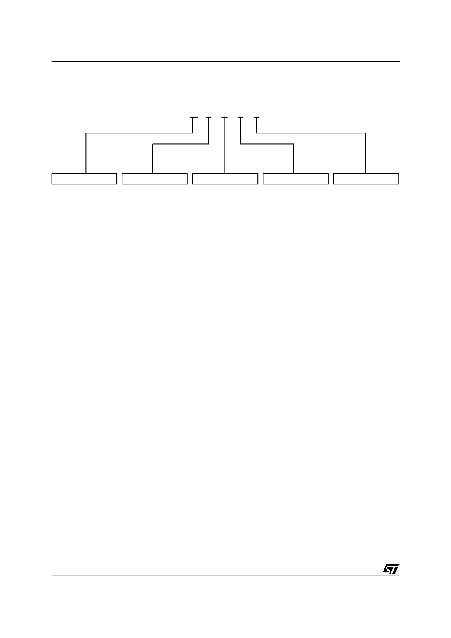
ORDERING INFORMATION SCHEME
Speed
90
(1)
90ns
12
120ns
15
150ns
20
200ns
25
(2)
250ns
Operating Voltage
blank
4.5V to 5.5V
W
2.7V to 3.6V
Package
BS PDIP28
KA PLCC32
MS SO28 300 mils
NS TSOP28
8 x 13.4mm
Temperature Range
1
(3)
0 to 70
∞
C
6
≠40 to 85
∞
C
Option
T
Tape & Reel
Packing
Example:
M28256 ≠ 15
W
KA
6
T
Notes: 1. Not available for "W" operating voltage.
2. Available for "W" operating voltage only.
3. Temperature Range on request only.
Devices are shipped from the factory with the memory content set at all "1's" (FFh).
For a list of available options (Speed, Package, etc...) or for further informationon any aspect of this device,
please contact the STMicroelectronics Sales Office nearest to you.
16/21
M28256

PDIP
A2
A1
A
L
B1
B
e1
D
S
E1
E
N
1
C
eA
eB
D2
Symb
mm
inches
Typ
Min
Max
Typ
Min
Max
A
≠
5.08
≠
0.200
A1
0.38
≠
0.015
≠
A2
3.56
4.06
0.140
0.160
B
0.38
0.51
0.015
0.020
B1
1.52
≠
≠
0.060
≠
≠
C
0.20
0.30
0.008
0.012
D
36.83
37.34
1.450
1.470
D2
33.02
≠
≠
1.300
≠
≠
E
15.24
≠
≠
0.600
≠
≠
E1
13.59
13.84
0.535
0.545
e1
2.54
≠
≠
0.100
≠
≠
eA
14.99
≠
≠
0.590
≠
≠
eB
15.24
17.78
0.600
0.700
L
3.18
3.43
0.125
0.135
S
1.78
2.08
0.070
0.082
0
∞
10
∞
0
∞
10
∞
N
28
28
Drawing is not to scale.
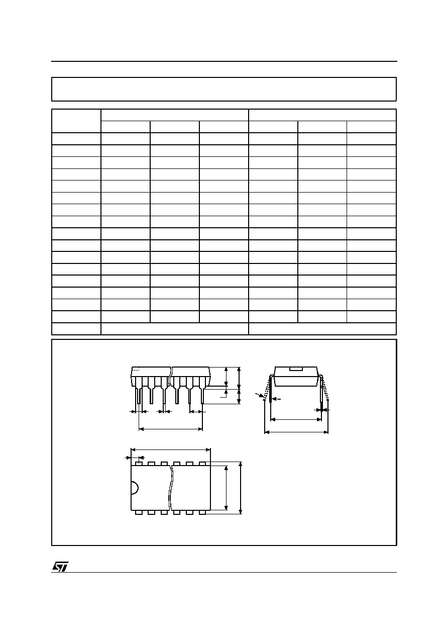
PDIP28 - 28 pin Plastic DIP, 600 mils width
17/21
M28256

PLCC
D
Ne
E1 E
1 N
D1
Nd
CP
B
D2/E2
e
B1
A1
A
R
0.51 (.020)
1.14 (.045)
F
A2
Symb
mm
inches
Typ
Min
Max
Typ
Min
Max
A
2.54
3.56
0.100
0.140
A1
1.52
2.41
0.060
0.095
A2
≠
0.38
≠
0.015
B
0.33
0.53
0.013
0.021
B1
0.66
0.81
0.026
0.032
D
12.32
12.57
0.485
0.495
D1
11.35
11.56
0.447
0.455
D2
9.91
10.92
0.390
0.430
E
14.86
15.11
0.585
0.595
E1
13.89
14.10
0.547
0.555
E2
12.45
13.46
0.490
0.530
e
1.27
≠
≠
0.050
≠
≠
F
0.00
0.25
0.000
0.010
R
0.89
≠
≠
0.035
≠
≠
N
32
32
Nd
7
7
Ne
9
9
Drawing is not to scale.
PLCC32 - 32 lead Plastic Leaded Chip Carrier, rectangular
18/21
M28256

SO-b
E
N
CP
B
e
A2
D
C
L
A1
H
A
1
Symb
mm
inches
Typ
Min
Max
Typ
Min
Max
A
2.46
2.64
0.097
0.104
A1
0.13
0.29
0.005
0.011
B
0.35
0.48
0.014
0.019
C
0.23
0.32
0.009
0.013
D
17.81
18.06
0.701
0.711
E
7.42
7.59
0.292
0.299
e
1.27
≠
≠
0.050
≠
≠
H
10.16
10.41
0.400
0.410
L
0.61
1.02
0.024
0.040
0
∞
8
∞
0
∞
8
∞
N
28
28
CP
0.10
0.004
Drawing is not to scale.
SO28 - 28 lead Plastic Small Outline, 300 mils body width
19/21
M28256

Symb
mm
inches
Typ
Min
Max
Typ
Min
Max
A
1.25
0.049
A1
0.20
0.008
A2
0.95
1.15
0.037
0.045
B
0.17
0.27
0.007
0.011
C
0.10
0.21
0.004
0.008
D
13.20
13.60
0.520
0.535
D1
11.70
11.90
0.461
0.469
E
7.90
8.10
0.311
0.319
e
0.55
-
-
0.022
-
-
L
0.50
0.70
0.020
0.028
0
∞
5
∞
0
∞
5
∞
N
28
28
CP
0.10
0.004
Drawing is not to scale.
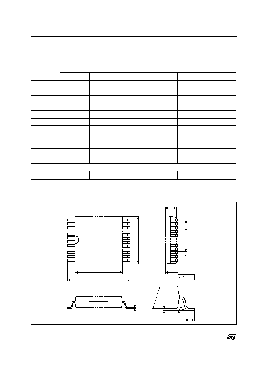
TSOP28 - 28 lead Plastic Thin Small Outline, 8 x 13.4mm
TSOP-c
D1
E
7
8
CP
B
e
A2
A
22
D
DIE
C
L
A1
21
28
1
20/21
M28256

Information furnished is believed to be accurate and reliable. However, STMicroelectronics assumes no responsibility for the consequences
of use of such information nor for any infringement of patents or other rights of third parties which may result from its use. No license is granted
by implication or otherwise under any patent or patent rights of STMicroelectronics. Spec ifications mentioned in this publication are subject to
change without notice. This publication supersedes and replaces all information previously supplied. STMicroelectronics products are not
authorized for use as critical components in life support devices or systems without express written approval of STMicroelectronics.
The ST logo is a registered trademark of STMicroelectronics
©
1999 STMicroelectronics - All Rights Reserved
STMicroelectronics GROUP OF COMPANIES
Australia - Brazil - Canada - China - France - Germany - Italy - Japan - Korea - Malaysia - Malta - Mexico - Morocco - The Netherlands -
Singapore - Spain - Sweden - Switzerland - Taiwan - Thailand - United Kingdom - U.S.A.
http://www.st.com
21/21
M28256

