M28C16
16K (2K x 8) PARALLEL EEPROM
with SOFTWARE DATA PROTECTION
NOT FOR NEW DESIGN
November 1997
1/18
This is information on a product still in production bu t not recommended for new de sign.
AI01518B
11
A0-A10
W
DQ0-DQ7
VCC
M28C16
G
E
VSS
8
RB *
Figure 1. Logic Diagram
A0 - A10
Address Input
DQ0 - DQ7
Data Input / Output
W
Write Enable
E
Chip Enable
G
Output Enable
RB
Ready / Busy
V
CC
Supply Voltage
V
SS
Ground
Table 1. Signal Names
FAST ACCESS TIME: 90ns
SINGLE 5V
�
10% SUPPLY VOLTAGE
LOW POWER CONSUMPTION
FAST WRITE CYCLE:
� 64 Bytes Page Write Operation
� Byte or Page Write Cycle: 3ms Max
ENHANCED END OF WRITE DETECTION:
� Data Polling
� Toggle Bit
PAGE LOAD TIMER STATUS BIT
HIGH RELIABILITY SINGLE POLYSILICON,
CMOS TECHNOLOGY:
� Endurance >100,000 Erase/Write Cycles
� Data Retention >40 Years
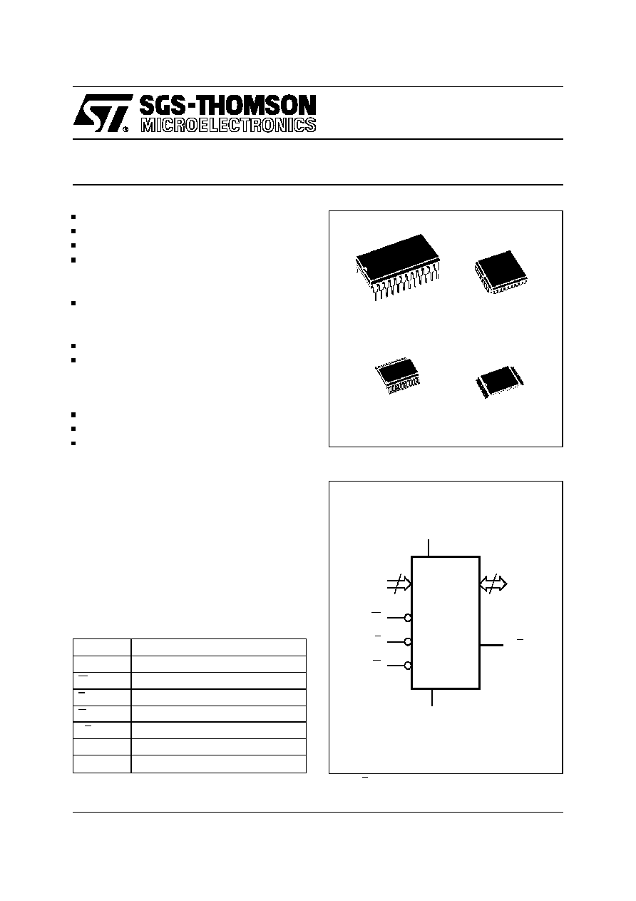
JEDEC APPROVED BYTEWIDE PIN OUT
SOFTWARE DATA PROTECTION
M28C16 is replaced by the products
described on the document M28C16A
DESCRIPTION
The M28C16 is a 2K x 8 low power Parallel
EEPROM fabricatedwith SGS-THOMSON proprie-
tary single polysilicon CMOS technology. The de-
vice offers fast access time with low power
dissipation and requires a 5V power supply. The
circuit has been designed to offer a flexible micro-
controller interface featuring both hardware and
software handshaking with Data Polling and Toggle
Bit. The M28C16 supports 64 byte page write op-
eration. A Software Data Protection (SDP) is also
possible using the standard JEDEC algorithm.
24
1
PDIP24 (P)
PLCC32 (K)
TSOP28 (N)
8 x13.4mm
24
1
SO24 (MS)
300 mils
Note: * RB function is offered only with TSOP28 package.
A1
A0
DQ0
A7
A4
A3
A2
A6
A5
A10
A8
A9
DQ7
W
G
E
DQ5
DQ1
DQ2
DQ3
VSS
DQ4
DQ6
VCC
AI01485
M28C16
8
1
2
3
4
5
6
7
9
10
11
12
13
14
16
15
24
23
22
21
20
19
18
17
Figure 2A. DIP Pin Connections
AI01486C
NC
A8
A10
DQ4
17
A0
NC
DQ0
DQ1
DQ2
DU
DQ3
A6
A3
A2
A1
A5
A4
9
W
A9
1
NC
NC
DQ6
A7
DQ7
32
DU
V
CC
M28C16
NC
NC
DQ5
G
E
25
V
SS
Figure 2B. LCC Pin Connections
Warning: NC = Not Connected, DU = Don't Use
DQ0
DQ1
A3
A0
A2
A1
A10
E
DQ7
G
DQ5
VCC
DQ4
A9
W
A4
A7
AI01519
M28C16
8
2
3
4
5
6
7
9
10
11
12
22
21
20
19
18
17
16
15
DQ2
VSS
A6
A5
DQ6
24
23
DQ3
1
A8
16
15
Figure 2C. SO Pin Connections
A1
A0
DQ0
A5
A2
A4
A3
A9
NC
DQ7
A8
G
E
DQ5
DQ1
DQ2
DQ3
DQ4
DQ6
NC
W
NC
A6
RB
VCC
A7
AI01175C
M28C16
28
1
22
7
8
14
15
21
VSS
A10
Figure 2D. TSOP Pin Connections
Warning: NC = Not Connected.
2/18
M28C16
Symbol
Parameter
Value
Unit
T
A
Ambient Operating Temperature
� 40 to 125
�
C
T
STG
Storage Temperature Range
� 65 to 150
�
C
V
CC
Supply Voltage
� 0.3 to 6.5
V
V
IO
Input/Output Voltage
� 0.3 to V
CC
+0.6
V
V
I
Input Voltage
� 0.3 to 6.5
V
V
ESD
Electrostatic Discharge Voltage (Human Body model)
(2)
4000
V
Notes: 1. Except for the rating "Operating Temperature Range", stresses above those listed in the Table "Absolute Maximum Ratings" may
cause permanent damage to the device. These are stress ratings only and operation of the device at these or any other conditions
above those indicated in the Operating sections of this specification is not implied. Exposure to Absolute Maximum Rating
conditions for extended periods may affect device reliability. Refer also to the SGS-THOMSON SURE Program and other
relevant quality documents.
2. 100pF through 1500
; MIL-STD-883C, 3015.7
Table 2. Absolute Maximum Ratings
(1)
PIN DESCRIPTION
Addresses (A0-A10). The address inputs select
an 8-bit memory location during a read or write
operation.
Chip Enable (E). The chip enable input must be
low to enable all read/write operations. When Chip
Enable is high, power consumption is reduced.
Output Enable (G). The Output Enable input con-
trols the data output buffers and is used to initiate
read operations.
Data In/ Out (DQ0 - DQ7). Data is written to or read
from the M28C16 through the I/O pins.
Write Enable (W). The Write Enable input controls
the writing of data to the M28C16.
Ready/Busy (RB). Ready/Busy is an open drain
output that can be used to detect the end of the
internal write cycle.
It is offered only with the TSOP28 package. The
reader should refer to the M28C17 datasheet for
more information about the Ready/Busy func-
tion.
OPERATION
In order to prevent data corruption and inadvertent
write operations an internal V
CC
comparator inhib-
its Write operation if V
CC
is below V
WI
(see Table
7). Access to the memory in write mode is allowed
after a power-up as specified in Table 7.
Read
The M28C16 is accessed like a static RAM. When
E and G are low with W high, the data addressed
is presented on the I/O pins. The I/O pins are high
impedance when either G or E is high.
Write
Write operations are initiated when both W and E
are low and G is high.The M28C16 supports both
E and W controlled write cycles. The Address is
latched by the falling edge of E or W which ever
occurs last and the Data on the rising edge of E or
W which ever occurs first. Once initiated the write
operation is internally timed until completion.
Mode
E
G
W
DQ0 - DQ7
Standby
1
X
X
Hi-Z
Output Disable
X
1
X
Hi-Z
Write Disable
X
X
1
Hi-Z
Read
0
0
1
Data Out
Write
0
1
0
Data In
Chip Erase
0
V
0
Hi-Z
Note: 1. 0 = V
IL
; 1 = V
IH
; X = V
IL
or V
IH;
V = 12
�
5%.
Table 3. Operating Modes
(1)
3/18
M28C16
Page Write
Page write allows up to 64 bytes to be consecu-
tively latched into the memory prior to initiating a
programming cycle. All bytes must be located in a
single page address, that is A6-A10 must be the
same for all bytes. The page write can be initiated
during any byte write operation.
Following the first byte write instruction the host
may send another address and data with a mini-
mum data transfer rate of 1/t
WHWH
(see Figure 13).
If a transition of E or W is not detected within t
WHWH
,
the internal programming cycle will start.
Chip Erase
The contents of the entire memory may be erased
to FFh by use of the Chip Erase command by
setting Chip Enable (E) Low and Output Enable
(G) to V
CC
+7V. The chip is cleared when a 10ms
low pulse is applied to the Write Enable pin.
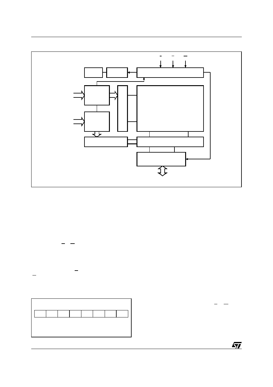
Microcontroller Control Interface
The M28C16 provides two write operation status
bits and one status pin that can be used to minimize
the system write cycle. These signals are available
on the I/O port bits DQ7 or DQ6 of the memory
during programming cycle only.
Data Polling bit (DQ7). During the internal write
cycle, any attempt to read the last byte written will
produce on DQ7 the complementary value of the
previously latched bit. Once the write cycle is fin-
ished the true logic value appears on DQ7 in the
read cycle.
Toggle bit (DQ6). The M28C16 offers another way
for determining when the internal write cycle is
completed. During the internal Erase/Write cycle,
DQ6 will toggle from "0" to "1" and "1" to "0" (the
first read value is "0") on subsequent attempts to
read the memory. When the internal cycle is com-
pleted the toggling will stop and the device will be
accessible for a new Read or Write operation.
Page Load Timer Status bit (DQ5). In the Page
Write mode data may be latched by E or W. Up to
64 bytes may be input. The Data output (DQ5)
indicates the status of the internal Page Load
Timer. DQ5 may be read by asserting Output En-
able Low (t
PLTS
). DQ5 Low indicates the timer is
running, High indicates time-out after which the
write cycle will start and no new data may be input.
DQ7 DQ6 DQ5 DQ4 DQ3 DQ2 DQ1 DQ0
DP
TB
PLTS Hi-Z
Hi-Z
Hi-Z
Hi-Z
Hi-Z
Figure 4. Status Bit Assignment
DP = Data Polling
TB = Toggle Bit
PLTS = Page Load Timer Status
AI01520
ADDRESS
LATCH
A6-A10
(Page Address)
X
DECODE
CONTROL LOGIC
64K ARRAY
ADDRESS
LATCH
A0-A5
Y DECODE
VPP GEN
RESET
SENSE AND DATA LATCH
I/O BUFFERS
E
G
W
PAGE LOAD
TIMER STATUS
TOGGLE BIT
DATA POLLING
DQ0-DQ7
Figure 3. Block Diagram
4/18
M28C16
Software Data Protection
The M28C16 offers a software controlled write
protection facility that allows the user to inhibit all
write modes to the device including the Chip Erase
instruction. This can be useful in protecting the
memory from inadvertent write cycles that may
occur due to uncontrolled bus conditions.
The M28C16 is shipped as standard in the "unpro-
tected" state meaning that the memory contents
can be changed as required by the user. After the
Software Data Protection enable algorithm is is-
sued, the device enters the "Protect Mode" of
operation where no further write commands have
any effect on the memory contents. The device
remains in this mode until a valid Software Data
Protection (SDP) disable sequence is received
whereby the device reverts to its "unprotected"
state. The Software Data Protection is fully non-
volatile and is not changed by power on/off se-
quences.
To enable the Software Data Protection (SDP) the
device requires the user to write (with a Page Write)
three specific data bytes to three specific memory
locations as per Figure 5. Similarly to disable the
Software Data Protection the user has to write
specific data bytes into six different locations as per
Figure 6 (with a Page Write). This complex series
ensures that the user will never enable or disable
the Software Data Protection accidentally.
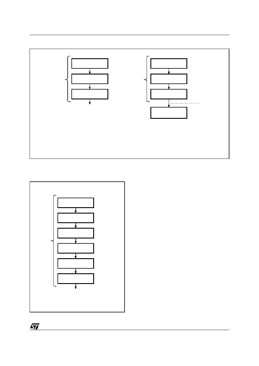
AI01509B
WRITE AAh in
Address 555h
WRITE 55h in
Address 2AAh
WRITE A0h in
Address 555h
SDP is set
WRITE AAh in
Address 555h
WRITE 55h in
Address 2AAh
WRITE A0h in
Address 555h
Write Page
(1 up to 64 bytes)
WRITE IN MEMORY
WHEN SDP IS SET
SDP ENABLE ALGORITHM
Page
Write
Instruction
(Note 1)
Page
Write
Instruction
(Note 1)
WRITE
is enabled
Figure 5. Software Data Protection Enable Algorithm and Memory Write
AI01510
WRITE AAh in
Address 555h
WRITE 55h in
Address 2AAh
WRITE 80h in
Address 555h
Unprotected State
WRITE AAh in
Address 555h
WRITE 55h in
Address 2AAh
WRITE 20h in
Address 555h
Page
Write
Instruction
Figure 6. Software Data Protection Disable
Algorithm
Note: 1. MSB Address bits (A6 to A10) differ during these specific Page Write operations.
5/18
M28C16