M28C16A
M28C17A
16 Kbit (2Kb x8) Parallel EEPROM
August 1998
1/19
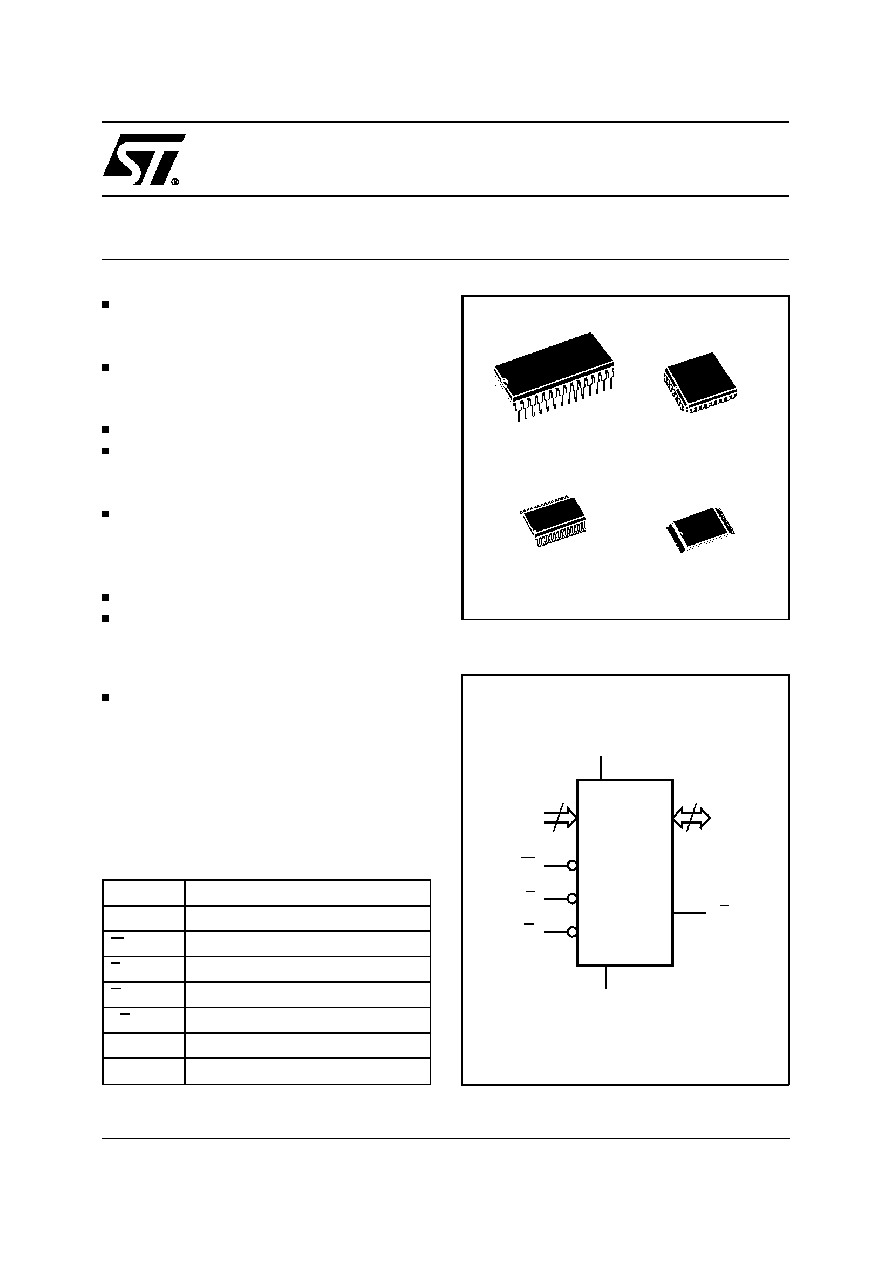
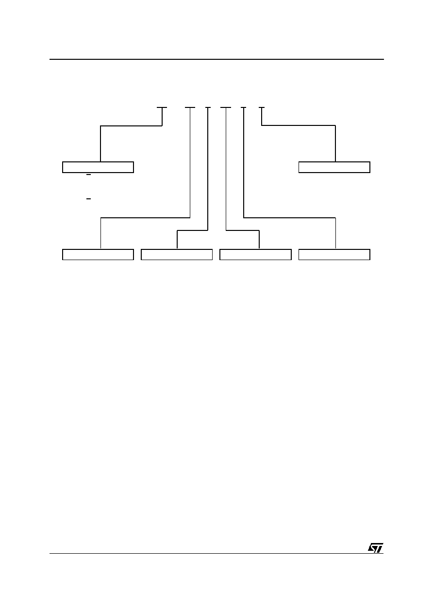
AI02109
11
A0-A10
W
DQ0-DQ7
VCC
M28C16A
M28C17A
G
E
VSS
8
RB
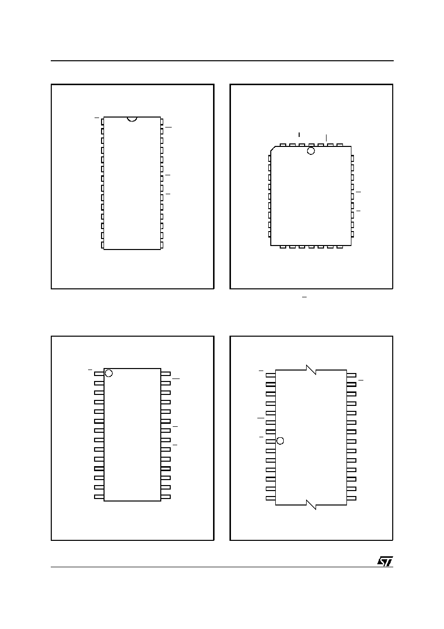
Figure 1. Logic Diagram
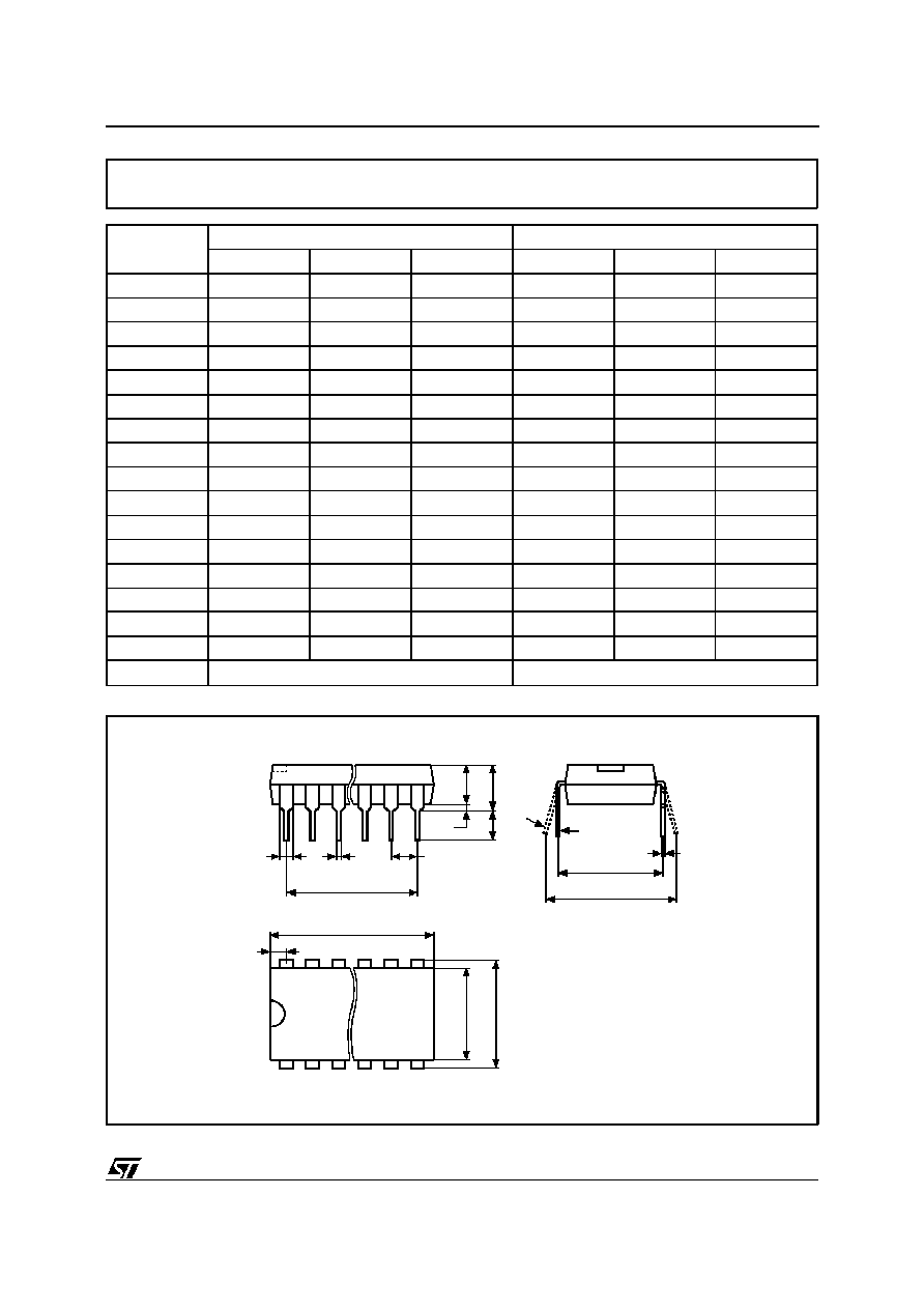
28
1
PDIP28 (BS)
PLCC32 (KA)
A0-A10
Address Input
DQ0-DQ7
Data Input / Output
W
Write Enable
E
Chip Enable
G
Output Enable
RB
Ready / Busy
V
CC
Supply Voltage
V
SS
Ground
Table 1. Signal Names
FAST ACCESS TIME:
≠ 150ns at 5V
≠ 250ns at 3V
SINGLE SUPPLY VOLTAGE:
≠ 5V
±
10% for M28C16A and M28C17A
≠ 2.7V to 3.6V for M28C16-xxW
LOW POWER CONSUMPTION
FAST WRITE CYCLE
≠ 32 Bytes Page Write Operation
≠ Byte or Page Write Cycle: 5ms
ENHANCED END OF WRITE DETECTION
≠ Ready/Busy Open Drain Output
≠ Data Polling
≠ Toggle Bit
PAGE LOAD TIMER STATUS BIT
HIGH RELIABILITY SINGLE POLYSILICON,
CMOS TECHNOLOGY
≠ Endurance >100,000 Erase/Write Cycles
≠ Data Retention >40 Years
JEDEC APPROVED BYTEWIDE PIN OUT
DESCRIPTION
The M28C16A and M28C17Aare 2K x8 low power
Parallel EEPROM fabricatedwith STMicroelectron-
ics proprietary single polysilicon CMOS technology.
The device offers fast access time with low power
dissipation and requires a 5V or 3V power supply.
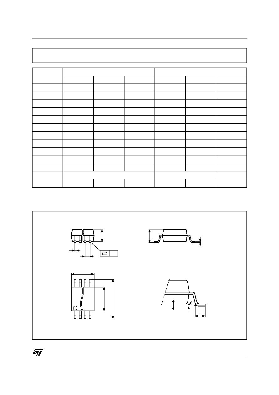
TSOP28 (NS)
8 x13.4mm
28
1
SO28 (MS)
300 mils
A1
A0
DQ0
A7
A4
A3
A2
A6
A5
DU
A10
A8
A9
DQ7
W
NC
G
E
DQ5
DQ1
DQ2
DQ3
VSS
DQ4
DQ6
NC
RB
VCC
AI02110
M28C17A
8
1
2
3
4
5
6
7
9
10
11
12
13
14
16
15
28
27
26
25
24
23
22
21
20
19
18
17
Figure 2A. DIP Pin Connections
Warning: NC = Not Connected, DU = Don't Use.
AI02111
DU
A8
A10
DQ4
17
A0
NC
DQ0
DQ1
DQ2
NC
DQ3
A6
A3
A2
A1
A5
A4
9
W
A9
1
RB
or
NC
(1)
NC
DQ6
A7
DQ7
32
DU
V
CC
M28C16A
M28C17A
NC
NC
DQ5
G
E
25
V
SS
Figure 2B. LCC Pin Connections
Warning: NC = Not Connected, DU = Don't Use.
Note: 1. Pin 2 is either RB for M28C17A or NC
for M28C16A.
A1
A0
DQ0
A5
A2
A4
A3
A9
NC
DQ7
A8
G
E
DQ5
DQ1
DQ2
DQ3
DQ4
DQ6
DU
W
NC
A6
RB
VCC
A7
AI02113
M28C16A
28
1
22
7
8
14
15
21
VSS
A10
Figure 2D. TSOP Pin Connections
Warning: NC = Not Connected, DU = Don't Use.
DQ0
DQ1
A3
A0
A2
A1
A10
E
DU
DQ7
G
DQ5
VCC
DQ4
A9
W
A4
RB
A7
AI02112
M28C17A
8
2
3
4
5
6
7
9
10
11
12
13
14
22
21
20
19
18
17
16
15
DQ2
VSS
A6
A5
DQ6
28
27
26
25
24
23
NC
DQ3
1
NC
A8
Figure 2C. SO Pin Connections
Warning: NC = Not Connected, DU = Don't Use.
2/19
M28C16A, M28C17A
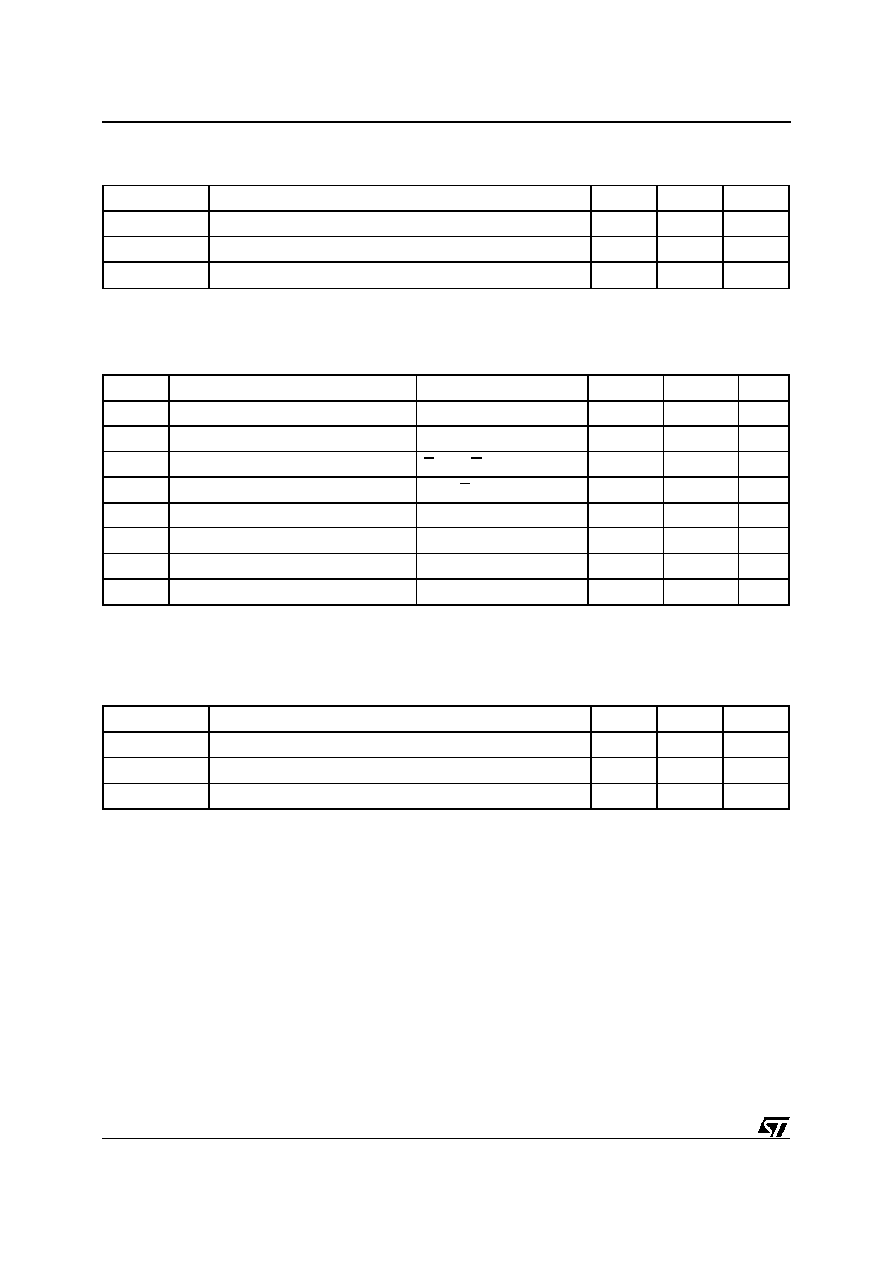
Symbol
Parameter
Value
Unit
T
A
Ambient Operating Temperature
(2)
≠ 40 to 85
∞
C
T
STG
Storage Temperature Range
≠ 65 to 150
∞
C
V
CC
Supply Voltage
≠ 0.3 to 6.5
V
V
IO
Input/Output Voltage
≠ 0.3 to V
CC
+0.6
V
V
I
Input Voltage
≠ 0.3 to 6.5
V
V
ESD
Electrostatic Discharge Voltage (Human Body model)
3000
V
Notes: 1. Except for the rating "Operating Temperature Range", stresses above those listed in the Table "Absolute Maximum Ratings"
may cause permanent damage to the device. These are stress ratings only and operation of the device at these or any other
conditions above those indicated in the Operating sections of this specification is not i mplied. Exposure to Absolute Maximum
Rating conditions for extended periods may affect device reliability. Refer also to the STMicroelectronics SURE Program and other
relevant quality documents.
2. Depends on range.
Table 2. Absolute Maximum Ratings
(1)
Mode
E
G
W
DQ0 - DQ7
Read
V
IL
V
IL
V
IH
Data Out
Write
V
IL
V
IH
V
IL
Data In
Standby / Write Inhibit
V
IH
X
X
Hi-Z
Write Inhibit
X
X
V
IH
Data Out or Hi-Z
Write Inhibit
X
V
IL
X
Data Out or Hi-Z
Output Disable
X
V
IH
X
Hi-Z
Note: X = V
IH
or V
IL
Table 3. Operating Modes
The circuit has been designed to offer a flexible
microcontroller interface featuring both hardware
and software handshakingmode with Ready/Busy,
Data Polling and Toggle Bit. The M28C16A/17A
supports 32 byte page write operation.
PIN DESCRITPION
Addresses (A0-A10). The address inputs select
an 8-bit memory location during a read or write
operation.
Chip Enable (E). The chip enable input must be
low to enable all read/write operations. When Chip
Enable is high, power consumption is reduced.
Output Enable (G). The Output Enable input con-
trols the data output buffers and is used to initiate
read operations.
Data In/ Out (DQ0 - DQ7). Data is written to or read
from the M28C16A/17A through the I/O pins.
Write Enable (W). The Write Enable input controls
the writing of data to the M28C16A/17A.
Ready/Busy (RB). Ready/Busy is an open drain
output that can be used to detect the end of the
internal write cycle. Ready/Busy is available for the
M28C17A in PDIP, PLCC and SO packages, and
for the M28C16A in TSOP only.
OPERATION
In order to prevent data corruption and inadvertent
write operations during power-up, a Power On
Reset (POR) circuit resets all internal programming
cicuitry. Access to the memory in write mode is
allowed after a power-up as specified in Table 7.
Read
The M28C16A/17Ais accessed like a static RAM.
When E and G are low with W high, the data
addressed is presented on the I/O pins. The I/O
pins are high impedancewhen either G or E is high.
DESCRIPTION (cont'd)
3/19
M28C16A, M28C17A
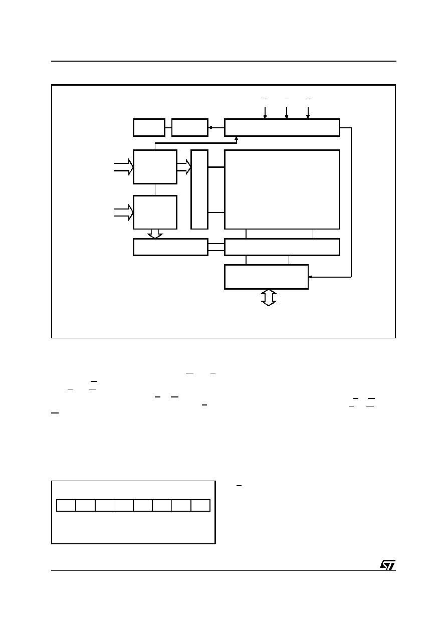
AI01520
ADDRESS
LATCH
A6-A10
(Page Address)
X
DECODE
CONTROL LOGIC
64K ARRAY
ADDRESS
LATCH
A0-A5
Y DECODE
VPP GEN
RESET
SENSE AND DATA LATCH
I/O BUFFERS
E
G
W
PAGE LOAD
TIMER STATUS
TOGGLE BIT
DATA POLLING
DQ0-DQ7
Figure 3. Block Diagram
Write
Write operations are initiated when both W and E
are low and G is high.The M28C16A/17Asupports
both E and W controlled write cycles. The Address
is latched by the falling edge of E or W which ever
occurs last and the Data on the rising edge of E or
W which ever occurs first. Once initiated the write
operation is internally timed until completion.
Page Write
Page write allows up to 32 bytes to be consecu-
tively latched into the memory prior to initiating a
DQ7
DQ6 DQ5 DQ4 DQ3 DQ2 DQ1 DQ0
DP
TB
PLTS Hi-Z
Hi-Z
Hi-Z
Hi-Z
Hi-Z
Figure 4. Status Bit Assignment
DP = Data Polling
TB = Toggle Bit
PLTS = Page Load Timer Status
programming cycle. All bytes must be located in a
single page address, that is A5 - A10 must be the
same for all bytes. The page write can be initiated
during any byte write operation.
Following the first byte write instruction the host
may send another address and data up to a maxi-
mum of t
WHWH
after the rising edge of E or W which
ever occurs first. If a transition of E or W is not
detected within t
WHWH
, the internal programming
cycle will start.
Microcontroller Control Interface
The M28C16A/17A provides two write operation
status bits and one status pin that can be used to
minimize the system write cycle. These signals are
available on the I/O port bits DQ7 or DQ6 of the
memory during programming cycle only, or as the
RB signal on a separate pin.
Data Polling bit (DQ7). During the internal write
cycle, any attempt to read the last byte written will
produce on DQ7 the complementary value of the
previously latched bit. Once the write cycle is fin-
ished the true logic value appears on DQ7 in the
read cycle.
OPERATION (cont'd)
4/19
M28C16A, M28C17A

Symbol
Parameter
Test Condition
Min
Max
Unit
C
IN
Input Capacitance
V
IN
= 0V
6
pF
C
OUT
Output Capacitance
V
OUT
= 0V
12
pF
Note: 1. Sampled only, not 100% tested.
Table 5. Capacitance
(1)
(T
A
= 25
∞
C, f = 1 MHz )
Symbol
Parameter
Test Condition
Min
Max
Unit
I
LI
Input Leakage Current
0V
V
IN
V
CC
10
µ
A
I
LO
Output Leakage Current
0V
V
IN
V
CC
10
µ
A
I
CC
(1)
Supply Current (TTL and CMOS inputs)
E = V
IL
, G = V
IL
, f = 5MHz
25
mA
I
CC1
(1)
Supply Current (Standby) TTL
E = V
IH
1
mA
I
CC2
(1)
Supply Current (Standby) CMOS
E > V
CC
≠ 0.3V
50
µ
A
V
IL
Input Low Voltage
≠0.3
0.8
V
V
IH
Input High Voltage
2
V
CC
+ 0.5
V
V
OL
Output Low Voltage
I
OL
= 2.1 mA
0.4
V
V
OH
Output High Voltage
I
OH
= ≠400
µ
A
2.4
V
Note: 1. All I/O's open circuit.
Table 6. Read Mode DC Characteristics for M28C16A and M28C17A
(T
A
= ≠40 to 85
∞
C, V
CC
= 4.5V to 5.5V)
Input Rise and Fall Times
20ns
Input Pulse Voltages
0.4V to 2.4V
Input and Output Timing Ref. Voltages
0.8V to 2.0V
Note that Output Hi-Z is defined as the point where data is no longer driven.
Table 4. AC Measurement Conditions
AI02101B
4.5V to 5.5V Operating Voltage
2.7V to 3.6V Operating Voltage
VCC ≠ 0.3V
0V
0.5 VCC
2.4V
0.4V
2.0V
0.8V
Figure 5. AC Testing Input Output Waveforms
AI02114
OUT
CL = 30pF
CL includes JIG capacitance
IOL
DEVICE
UNDER
TEST
IOH
VCC
Figure 6. AC Testing Equivalent Load Circuit
5/19
M28C16A, M28C17A
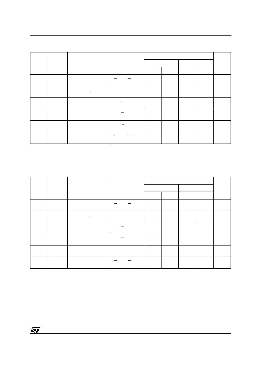
Symbol
Parameter
Test Condition
Min
Max
Unit
I
LI
Input Leakage Current
0V
V
IN
V
CC
10
µ
A
I
LO
Output Leakage Current
0V
V
IN
V
CC
10
µ
A
I
CC
(1)
Supply Current (TTL and CMOS inputs)
E = V
IL
, G = V
IL
, f = 5 MHz
15
mA
I
CC2
(1)
Supply Current (Standby) CMOS
E > V
CC
≠0.3V
20
µ
A
V
IL
Input Low Voltage
≠0.3
0.6
V
V
IH
Input High Voltage
2
V
CC
+ 0.5
V
V
OL
Output Low Voltage
I
OL
= 2.1 mA
0.2 V
CC
V
V
OH
Output High Voltage
I
OH
= ≠400
µ
A
0.8 V
CC
V
Note: 1. All I/O's open circuit.
Table 8. Read Mode DC Characteristics for M28C16A-W
(T
A
= ≠40 to 85
∞
C, V
CC
= 2.7V to 3.6V)
Symbol
Parameter
Min
Max
Unit
t
PUR
Time Delay to Read Operation
1
µ
s
t
PUW
Time Delay to Write Operation (once V
CC
V
WI
)
10
ms
V
WI
Write Inhibit Threshold
1.5
2.5
V
Note: 1. Sampled only, not 100% tested.
Table 9. Power Up Timing for M28C16A-W
(1)
(T
A
= ≠40 to 85
∞
C, V
CC
= 2.7V to 3.6V)
Symbol
Parameter
Min
Max
Unit
t
PUR
Time Delay to Read Operation
1
µ
s
t
PUW
Time Delay to Write Operation (once V
CC
V
WI
)
10
ms
V
WI
Write Inhibit Threshold
1.5
2.5
V
Note: 1. Sampled only, not 100% tested.
Table 7. Power Up Timing for M28C16A and M28C17A
(1)
(T
A
= ≠40 to 85
∞
C, V
CC
= 4.5V to 5.5V)
6/19
M28C16A, M28C17A
Symbol
Alt
Parameter
Test Condition
M28C16A / M28C17A
Unit
-15
-20
min
max
min
max
t
AVQV
t
ACC
Address Valid to
Output Valid
E = V
IL
, G = V
IL
150
200
ns
t
ELQV
t
CE
Chip Enable Low to
Output Valid
G = V
IL
150
200
ns
t
GLQV
t
OE
Output Enable Low to
Output Valid
E = V
IL
70
80
ns
t
EHQZ
(1)
t
DF
Chip Enable High to
Output Hi-Z
G = V
IL
0
50
0
60
ns
t
GHQZ
(1)
t
DF
Output Enable High to
Output Hi-Z
E = V
IL
0
50
0
60
ns
t
AXQX
t
OH
Address Transition to
Output Transition
E = V
IL
, G = V
IL
0
0
ns
Note: 1. Output Hi-Z is defined as the point at which data is no longer driven.
Table 10. Read Mode AC Characteristics for M28C16A and M28C17A
(T
A
= ≠40 to 85
∞
C, V
CC
= 4.5V to 5.5V)
Symbol
Alt
Parameter
Test Condition
M28C16A / M28C17A
Unit
-25
-30
min
max
min
max
t
AVQV
t
ACC
Address Valid to
Output Valid
E = V
IL
, G = V
IL
250
300
ns
t
ELQV
t
CE
Chip Enable Low to
Output Valid
G = V
IL
250
300
ns
t
GLQV
t
OE
Output Enable Low to
Output Valid
E = V
IL
100
100
ns
t
EHQZ
(1)
t
DF
Chip Enable High to
Output Hi-Z
G = V
IL
0
70
0
80
ns
t
GHQZ
(1)
t
DF
Output Enable High to
Output Hi-Z
E = V
IL
0
70
0
80
ns
t
AXQX
t
OH
Address Transition to
Output Transition
E = V
IL
, G = V
IL
0
0
ns
Note: 1. Output Hi-Z is defined as the point at which data is no longer driven.
Table 11. Read Mode AC Characteristics for M28C16-W
(T
A
= ≠40 to 85
∞
C, V
CC
= 2.7V to 3.6V)
7/19
M28C16A, M28C17A
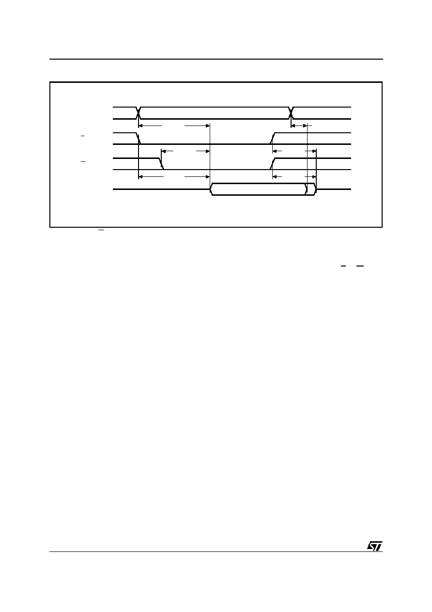
AI01511B
VALID
tAVQV
tAXQX
tGLQV
tEHQZ
tGHQZ
DATA OUT
A0-A10
E
G
DQ0-DQ7
tELQV
Hi-Z
Figure 7. Read Mode AC Waveforms
Toggle bit (DQ6). The M28C16A/17A offers an-
other way for determining when the internal write
cycle is completed. During the internal Erase/Write
cycle, DQ6 will toggle from "0" to "1" and "1" to "0"
(the first read value is "0") on subsequentattempts
to read any address in the memory. When the
internalcycle is completed the togglingwill stopand
the device will be accessible for a new Read or
Write operation.
Page Load Timer Status bit (DQ5). In the Page
Write mode data may be latched by E or W up to
t
WHWH
after the previous byte. Up to 32 bytes may
be input. The Data output (DQ5) indicates the
status of the internal Page Load Timer. DQ5 may
be read by asserting Output Enable Low (t
PLTS
).
DQ5 Low indicates the timer is running,
High
Note: Write Enable (W) = High
8/19
M28C16A, M28C17A
Symbol
Alt
Parameter
Test Condition
Min
Max
Unit
t
AVWL
t
AS
Address Valid to Write Enable Low
E = V
IL
, G = V
IH
0
ns
t
AVEL
t
AS
Address Valid to Chip Enable Low
G = V
IH
, W = V
IL
0
ns
t
ELWL
t
CES
Chip Enable Low to Write Enable Low
G = V
IH
0
ns
t
GHWL
t
OES
Output Enable High to Write Enable
Low
E = V
IL
0
ns
t
GHEL
t
OES
Output Enable High to Chip Enable Low
W = V
IL
0
ns
t
WLEL
t
WES
Write Enable Low to Chip Enable Low
G = V
IH
0
ns
t
WLAX
t
AH
Write Enable Low to Address Transition
100
ns
t
ELAX
t
AH
Chip Enable Low to Address Transition
100
ns
t
WLDV
t
DV
Write Enable Low to Input Valid
E = V
IL
, G = V
IH
1
µ
s
t
ELDV
t
DV
Chip Enable Low to Input Valid
G = V
IH
, W = V
IL
1
µ
s
t
ELEH
t
WP
Chip Enable Low to Chip Enable High
100
ns
t
WHEH
t
CEH
Write Enable High to Chip Enable High
0
ns
t
WHGL
t
OEH
Write Enable High to Output Enable
Low
0
ns
t
EHGL
t
OEH
Chip Enable High to Output Enable Low
0
ns
t
EHWH
t
WEH
Chip Enable High to Write Enable High
0
ns
t
WHDX
t
DH
Write Enable High to Input Transition
0
ns
t
EHDX
t
DH
Chip Enable High to Input Transition
0
ns
t
WHWL
t
WPH
Write Enable High to Write Enable Low
200
ns
t
WLWH
tWP
Write Enable Low to Write Enable High
100
ns
t
WHWH
t
BLC
Byte Load Repeat Cycle Time
0.2
30
µ
s
t
WHRH
t
WC
Write Cycle Time
5
ms
t
WHRL
t
DB
Write Enable High to Ready/Busy Low
Note 1
100
ns
t
EHRL
t
DB
Chip Enable High to Ready/Busy Low
Note 1
100
ns
t
DVWH
t
DS
Data Valid before Write Enable High
50
ns
t
DVEH
t
DS
Data Valid before Chip Enable High
50
ns
Note: 1. With a 3.3 k
external pull-up resistor.
Table 12. Write Mode AC Characteristics for M28C16A and M28C17A
(T
A
= ≠40 to 85
∞
C, V
CC
= 4.5V to 5.5V)
9/19
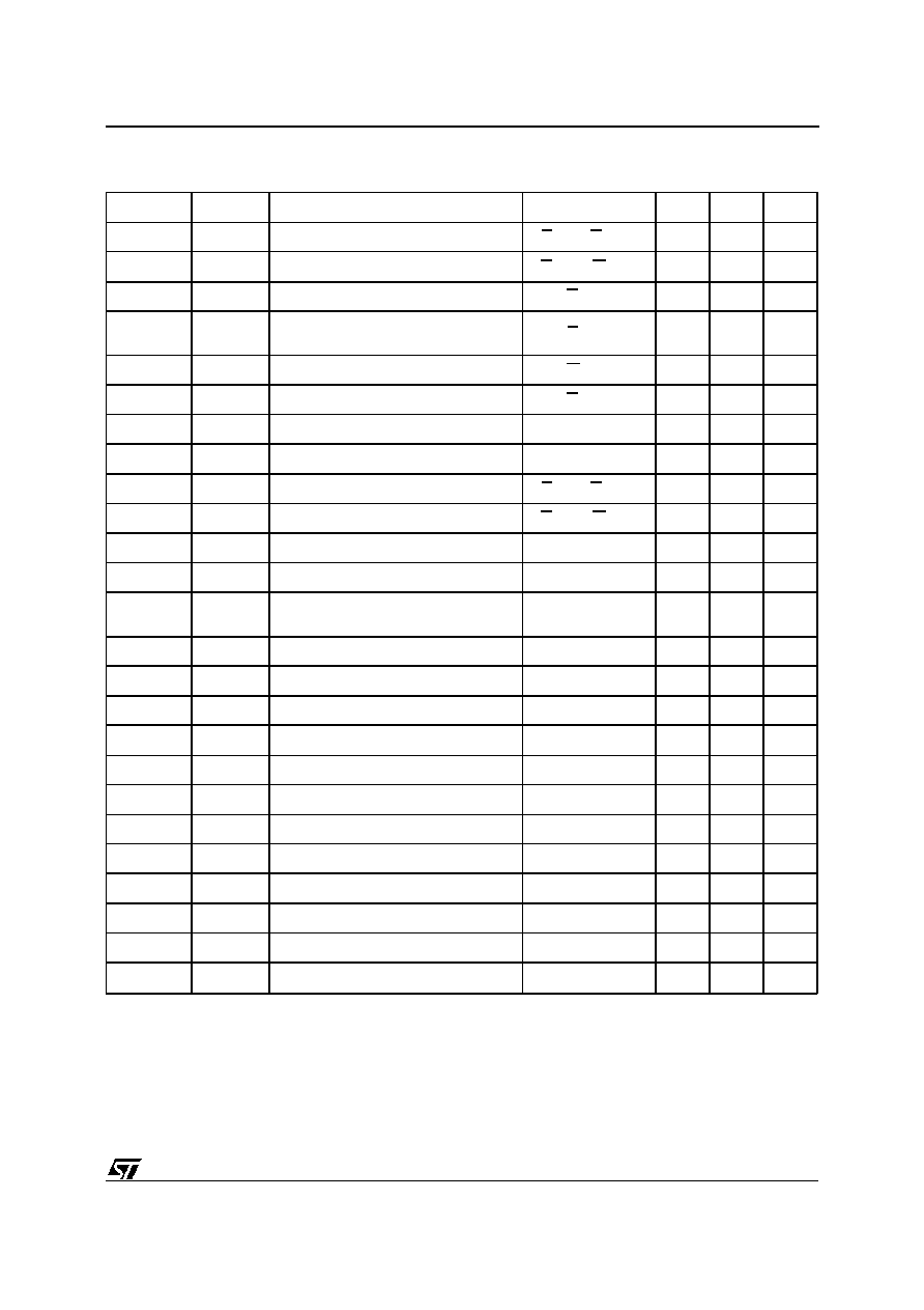
M28C16A, M28C17A
Symbol
Alt
Parameter
Test Condition
Min
Max
Unit
t
AVWL
t
AS
Address Valid to Write Enable Low
E = V
IL
, G = V
IH
0
ns
t
AVEL
t
AS
Address Valid to Chip Enable Low
G = V
IH
, W = V
IL
0
ns
t
ELWL
t
CES
Chip Enable Low to Write Enable Low
G = V
IH
0
ns
t
GHWL
t
OES
Output Enable High to Write Enable
Low
E = V
IL
0
ns
t
GHEL
t
OES
Output Enable High to Chip Enable Low
W = V
IL
0
ns
t
WLEL
t
WES
Write Enable Low to Chip Enable Low
G = V
IH
0
ns
t
WLAX
t
AH
Write Enable Low to Address Transition
200
ns
t
ELAX
t
AH
Chip Enable Low to Address Transition
200
ns
t
WLDV
t
DV
Write Enable Low to Input Valid
E = V
IL
, G = V
IH
1
µ
s
t
ELDV
t
DV
Chip Enable Low to Input Valid
G = V
IH
, W = V
IL
1
µ
s
t
ELEH
t
WP
Chip Enable Low to Chip Enable High
200
ns
t
WHEH
t
CEH
Write Enable High to Chip Enable High
0
ns
t
WHGL
t
OEH
Write Enable High to Output Enable
Low
0
ns
t
EHGL
t
OEH
Chip Enable High to Output Enable Low
0
ns
t
EHWH
t
WEH
Chip Enable High to Write Enable High
0
ns
t
WHDX
t
DH
Write Enable High to Input Transition
0
ns
t
EHDX
t
DH
Chip Enable High to Input Transition
0
ns
t
WHWL
t
WPH
Write Enable High to Write Enable Low
200
ns
t
WLWH
tWP
Write Enable Low to Write Enable High
200
ns
t
WHWH
t
BLC
Byte Load Repeat Cycle Time
0.4
50
µ
s
t
WHRH
t
WC
Write Cycle Time
5
ms
t
WHRL
t
DB
Write Enable High to Ready/Busy Low
Note 1
250
ns
t
EHRL
t
DB
Chip Enable High to Ready/Busy Low
Note 1
250
ns
t
DVWH
t
DS
Data Valid before Write Enable High
50
ns
t
DVEH
t
DS
Data Valid before Chip Enable High
50
ns
Note: 1. With a 3.3 k
external pull-up resistor.
Table 13. Write Mode AC Characteristics for M28C16-W
(T
A
= ≠40 to 85
∞
C, V
CC
= 2.7V to 3.6V)
10/19
M28C16A, M28C17A
AI01512
VALID
tAVWL
A0-A10
E
G
DQ0-DQ7
DATA IN
W
tWLAX
tELWL
tGHWL
tWLDV
tWHEH
tWHGL
tWLWH
tWHWL
tWHDX
tDVWH
RB
tWHRL
Figure 8. Write Mode AC Waveforms - Write Enable Controlled
AI01513
VALID
tAVEL
A0-A10
E
G
DQ0-DQ7
DATA IN
W
tELAX
tGHEL
tWLEL
tELDV
tEHGL
tEHDX
tDVEH
RB
tEHRL
tELEH
tEHWH
Figure 9. Write Mode AC Waveforms - Chip Enable Controlled
11/19
M28C16A, M28C17A
AI01514
A0-A10
E
G
DQ0-DQ7
W
tWHWH
Addr 0
DQ5
RB
Addr 1
Addr 2
Addr n
tWHWH
tWHRH
tWLWH
tWHWL
tPLTS
tWHRL
Byte 0
Byte 1
Byte 2
Byte n
Byte n
Figure 10. Page Write Mode AC Waveforms - Write Enable Controlled
AI01516
A0-A10
E
G
DQ7
W
DQ7
DQ7
DQ7
DQ7
DQ7
READY
LAST WRITE
INTERNAL WRITE SEQUENCE
Address of the last byte of the Page Write instruction
Figure 11. Data Polling Waveform Sequence
12/19
M28C16A, M28C17A
AI01517
A0-A10
E
G
DQ6
W
READY
LAST WRITE
INTERNAL WRITE SEQUENCE
(1)
TOGGLE
Figure 12. Toggle Bit Waveform Sequence
Note: 1. First Toggle bit is forced to '0'
13/19
M28C16A, M28C17A
Device Identifier
C16 RB available only
for the TSOP
package
C17 RB available
Speed
15
(1)
150 ns
20
(1)
200 ns
25
(2)
250ns
30
(2)
300ns
Operating Voltage
blank 4.5V to 5.5V
5ms write
W
2.7V to 3.6V
5ms write
Package
BS PDIP28
MS SO28
300 mils
NS TSOP28
8 x 13.4mm
KA PLCC32
Option
T
Tape & Reel
Packing
Temperature Range
6
≠40 to 85
∞
C
Example:
M28C16 ≠
20
W
NS
6
T
Notes: 1. Available for M28C16A and M28C17A only.
2. Available for "W" Operating Voltage only.
Devices are shipped from the factory with the memory content set at all "1's" (FFh).
For a list of available options (Speed, Package,etc... ) or for further informationon any aspect of this device,
please contact the STMicroelectronics Sales Office nearest to you.
ORDERING INFORMATION SCHEME
14/19
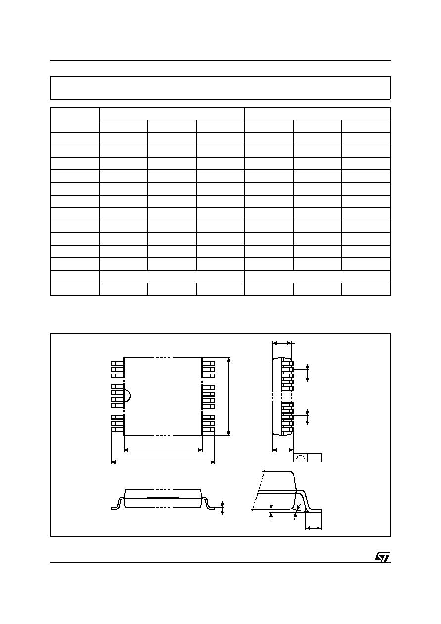
M28C16A, M28C17A
PDIP
A2
A1
A
L
B1
B
e1
D
S
E1
E
N
1
C
eA
eB
D2
Symb
mm
inches
Typ
Min
Max
Typ
Min
Max
A
≠
5.08
≠
0.200
A1
0.38
≠
0.015
≠
A2
3.56
4.06
0.140
0.160
B
0.38
0.51
0.015
0.020
B1
1.52
≠
≠
0.060
≠
≠
C
0.20
0.30
0.008
0.012
D
36.83
37.34
1.450
1.470
D2
33.02
≠
≠
1.300
≠
≠
E
15.24
≠
≠
0.600
≠
≠
E1
13.59
13.84
0.535
0.545
e1
2.54
≠
≠
0.100
≠
≠
eA
14.99
≠
≠
0.590
≠
≠
eB
15.24
17.78
0.600
0.700
L
3.18
3.43
0.125
0.135
S
1.78
2.08
0.070
0.082
0
∞
10
∞
0
∞
10
∞
N
28
28
Drawing is not to scale.
PDIP28 - 28 pin Plastic DIP, 600 mils width
15/19
M28C16A, M28C17A

PLCC
D
Ne
E1 E
1 N
D1
Nd
CP
B
D2/E2
e
B1
A1
A
R
0.51 (.020)
1.14 (.045)
F
A2
Symb
mm
inches
Typ
Min
Max
Typ
Min
Max
A
2.54
3.56
0.100
0.140
A1
1.52
2.41
0.060
0.095
A2
≠
0.38
≠
0.015
B
0.33
0.53
0.013
0.021
B1
0.66
0.81
0.026
0.032
D
12.32
12.57
0.485
0.495
D1
11.35
11.56
0.447
0.455
D2
9.91
10.92
0.390
0.430
E
14.86
15.11
0.585
0.595
E1
13.89
14.10
0.547
0.555
E2
12.45
13.46
0.490
0.530
e
1.27
≠
≠
0.050
≠
≠
F
0.00
0.25
0.000
0.010
R
0.89
≠
≠
0.035
≠
≠
N
32
32
Nd
7
7
Ne
9
9
CP
0.10
0.004
Drawing is not to scale.
PLCC32 - 32 lead Plastic Leaded Chip Carrier, rectangular
16/19
M28C16A, M28C17A
SO-b
E
N
CP
B
e
A2
D
C
L
A1
H
A
1
Symb
mm
inches
Typ
Min
Max
Typ
Min
Max
A
2.46
2.64
0.097
0.104
A1
0.13
0.29
0.005
0.011
A2
2.29
2.39
0.090
0.094
B
0.35
0.48
0.014
0.019
C
0.23
0.32
0.009
0.013
D
17.81
18.06
0.701
0.711
E
7.42
7.59
0.292
0.299
e
1.27
≠
≠
0.050
≠
≠
H
10.16
10.41
0.400
0.410
L
0.61
1.02
0.024
0.040
0
∞
8
∞
0
∞
8
∞
N
28
28
CP
0.10
0.004
Drawing is not to scale.
SO28 - 28 lead Plastic Small Outline, 300 mils body width
17/19
M28C16A, M28C17A
Symb
mm
inches
Typ
Min
Max
Typ
Min
Max
A
1.25
0.049
A1
0.20
0.008
A2
0.95
1.15
0.037
0.045
B
0.17
0.27
0.007
0.011
C
0.10
0.21
0.004
0.008
D
13.20
13.60
0.520
0.535
D1
11.70
11.90
0.461
0.469
E
7.90
8.10
0.311
0.319
e
0.55
-
-
0.022
-
-
L
0.50
0.70
0.020
0.028
0
∞
5
∞
0
∞
5
∞
N
28
28
CP
0.10
0.004
Drawing is not to scale.
TSOP28 - 28 lead Plastic Thin Small Outline, 8 x 13.4mm
TSOP-c
D1
E
7
8
CP
B
e
A2
A
22
D
DIE
C
L
A1
21
28
1
18/19
M28C16A, M28C17A

Information furnished is believed to be accurate and reliable. However, STMicroelectronics assumes no responsibility for the consequences
of use of such information nor for any infringement of patents or other rights of third parties which may result from its use. No license is granted
by implication or otherwise under any patent or patent rights of STMicroelectronics. Spec ifications mentioned in this publication are subject to
change without notice. This publication supersedes and replaces all information previously supplied. STMicroelectronics products are not
authorized for use as critical components in life support devices or systems without express written approval of STMicroelectronics.
©
1998 STMicroelectronics - All Rights Reserved
STMicroelectronics GROUP OF COMPANIES
Australia - Brazil - Canada - China - France - Germany - Italy - Japan - Korea - Malaysia - Malta - Mexico - Morocco - The Netherlands -
Singapore - Spain - Sweden - Switzerland - Taiwan - Thailand - United Kingdom - U.S.A.
19/19
M28C16A, M28C17A