1/24
June 2000
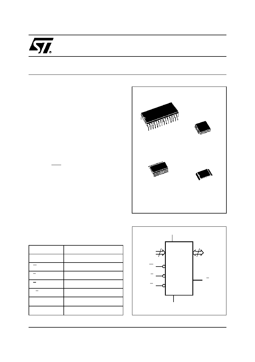
M28C64
64 Kbit (8K x 8) Parallel EEPROM
With Software Data Protection
s
Fast Access Time:
≠ 90 ns at V
CC
=5 V for M28C64 and M28C64-A
≠ 120 ns at V
CC
=3 V for M28C64-xxW
s
Single Supply Voltage:
≠ 4.5 V to 5.5 V for M28C64 and M28C64-A
≠ 2.7 V to 3.6 V for M28C64-xxW
s
Low Power Consumption
s
Fast BYTE and PAGE WRITE (up to 64 Bytes)
≠ 1 ms at V
CC
=4.5 V for M28C64-A
≠ 3 ms at V
CC
=4.5 V for M28C64
≠ 5 ms at V
CC
=2.7 V for M28C64-xxW
s
Enhanced Write Detection and Monitoring:
≠ Ready/Busy Open Drain Output
≠ Data Polling
≠ Toggle Bit
≠ Page Load Timer Status
s
JEDEC Approved Bytewide Pin-Out
s
Software Data Protection
s
100000 Erase/Write Cycles (minimum)
s
Data Retention (minimum):
≠ 40 Years for M28C64 and M28C64-xxW
≠ 10 Years for M28C64-A
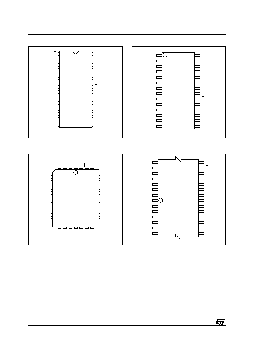
Figure 1. Logic Diagram
AI01350C
13
A0-A12
W
DQ0-DQ7
VCC
M28C64
G
E
VSS
8
RB
Table 1. Signal Names
A0-A12
Address Input
DQ0-DQ7
Data Input / Output
W
Write Enable
E
Chip Enable
G
Output Enable
RB
Ready / Busy
VCC
Supply Voltage
VSS
Ground
PDIP28 (BS)
SO28 (MS)
300 mil width
PLCC32 (KA)
28
1
TSOP28 (NS)
8 x 13.4 mm
28
1
M28C64
2/24
Figure 2A. DIP Connections
Note: 1. NC = Not Connected
Figure 2B. PLLC Connections
Note: 1. NC = Not Connected
2. DU = Do Not Use
A1
A0
DQ0
A7
A4
A3
A2
A6
A5
NC
A10
A8
A9
DQ7
W
A11
G
E
DQ5
DQ1
DQ2
DQ3
VSS
DQ4
DQ6
A12
RB
VCC
AI01351C
M28C64
8
1
2
3
4
5
6
7
9
10
11
12
13
14
16
15
28
27
26
25
24
23
22
21
20
19
18
17
AI01352D
NC
A8
A10
DQ4
17
A0
NC
DQ0
DQ1
DQ2
DU
DQ3
A6
A3
A2
A1
A5
A4
9
W
A9
1
RB
A11
DQ6
A7
DQ7
32
DU
V
CC
M28C64
A12
NC
DQ5
G
E
25
V
SS
Figure 2C. SO Connections
Note: 1. NC = Not Connected
Figure 2D. TSOP Connections
Note: 1. NC = Not Connected
DQ0
DQ1
A3
A0
A2
A1
A10
E
NC
DQ7
G
DQ5
VCC
DQ4
A9
W
A4
RB
A7
AI01353C
M28C64
8
2
3
4
5
6
7
9
10
11
12
13
14
22
21
20
19
18
17
16
15
DQ2
VSS
A6
A5
DQ6
28
27
26
25
24
23
A11
DQ3
1
A12
A8
A1
A0
DQ0
A5
A2
A4
A3
A9
A11
DQ7
A8
G
E
DQ5
DQ1
DQ2
DQ3
DQ4
DQ6
NC
W
A12
A6
RB
VCC
A7
AI01354C
M28C64
28
1
22
7
8
14
15
21
VSS
A10
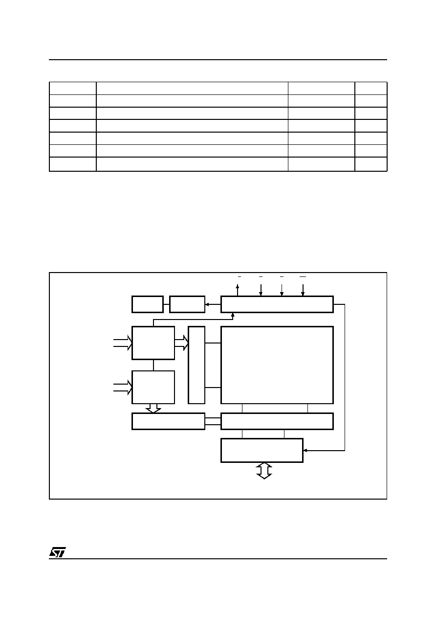
DESCRIPTION
The M28C64 devices consist of 8192x8 bits of low
power,
parallel
EEPROM,
fabricated
with
STMicroelectronics' proprietary single polysilicon
CMOS technology. The devices offer fast access
time, with low power dissipation, and require a
single voltage supply (5V or 3V, depending on the
option chosen).
The device has been designed to offer a flexible
microcontroller interface, featuring both hardware
and software handshaking, with Ready/Busy,
Data Polling and Toggle Bit. The device supports
a 64 byte Page Write operation. Software Data
Protection (SDP) is also supported, using the
standard JEDEC algorithm.
3/24
M28C64
Figure 3. Block Diagram
AI01355
ADDRESS
LATCH
A6-A12
(Page Address)
X
DECODE
CONTROL LOGIC
64K ARRAY
ADDRESS
LATCH
A0-A5
Y DECODE
VPP GEN
RESET
SENSE AND DATA LATCH
I/O BUFFERS
RB
E
G
W
PAGE LOAD
TIMER STATUS
TOGGLE BIT
DATA POLLING
DQ0-DQ7
Table 2. Absolute Maximum Ratings
1
Note: 1. Except for the rating "Operating Temperature Range", stresses above those listed in the Table "Absolute Maximum Ratings" may
cause permanent damage to the device. These are stress ratings only, and operation of the device at these or any other conditions
above those indicated in the Operating sections of this specification is not implied. Exposure to Absolute Maximum Rating condi-
tions for extended periods may affect device reliability. Refer also to the ST SURE Program and other relevant quality documents.
2. MIL-STD-883C, 3015.7 (100 pF, 1500
)
Symbol
Parameter
Value
Unit
T
A
Ambient Operating Temperature
-40 to 125
∞
C
T
STG
Storage Temperature
-65 to 150
∞
C
V
CC
Supply Voltage
-0.3 to V
CC
+1
V
V
IO
Input or Output Voltage
-0.6 to V
CC
+0.6
V
V
I
Input Voltage
-0.3 to 6.5
V
V
ESD
Electrostatic Discharge Voltage (Human Body model)
2
4000
V

M28C64
4/24
Table 3. Operating Modes
1
Note: 1. 0=
V
IL
; 1=
V
IH
; X =
V
IH
or V
IL
; V=12V
±
5%.
Mode
E
G
W
DQ0-DQ7
Stand-by
1
X
X
Hi-Z
Output Disable
X
1
X
Hi-Z
Write Disable
X
X
1
Hi-Z
Read
0
0
1
Data Out
Write
0
1
0
Data In
Chip Erase
0
V
0
Hi-Z
SIGNAL DESCRIPTION
The external connections to the device are
summarized in Table 1, and their use in Table 3.
Addresses (A0-A12). The address inputs are
used to select one byte from the memory array
during a read or write operation.
Data In/Out (DQ0-DQ7). The contents of the data
byte are written to, or read from, the memory array
through the Data I/O pins.
Chip Enable (E). The chip enable input must be
held low to enable read and write operations.
When Chip Enable is high, power consumption is
reduced.
Output Enable (G). The Output Enable input
controls the data output buffers, and is used to
initiate read operations.
Write Enable (W). The Write Enable input controls
whether the addressed location is to be read, from
or written to.
Ready/Busy (RB). Ready/Busy is an open drain
output that can be used to detect the end of the
internal write cycle.
DEVICE OPERATION
In order to prevent data corruption and inadvertent
write operations, an internal V
CC
comparator
inhibits the Write operations if the V
CC
voltage is
lower than V
WI
(see Table 4A and Table 4B). Once
the voltage applied on the V
CC
pin goes over the
V
WI
threshold (V
CC
>V
WI
), write access to the
memory is allowed after a time-out t
PUW
, as
specified in Table 4A and Table 4B.
Further protection against data corruption is
offered by the E and W low pass filters: any glitch,
on the E and W inputs, with a pulse width less than
10 ns (typical) is internally filtered out to prevent
inadvertent write operations to the memory.
Table 4A. Power-Up Timing
1
for M28C64 (5V range)
(T
A
= 0 to 70
∞
C or ≠40 to 85
∞
C or ≠40 to 125
∞
C; V
CC
= 4.5 to 5.5 V)
Note: 1. Sampled only, not 100% tested.
Table 4B. Power-Up Timing
1
for M28C64-xxW (3V range)
(T
A
= 0 to 70
∞
C or ≠40 to 85
∞
C; V
CC
= 2.7 to 3.6 V)
Note: 1. Sampled only, not 100% tested.
Symbol
Parameter
Min.
Max.
Unit
t
PUR
Time Delay to Read Operation
1
µ
s
t
PUW
Time Delay to Write Operation (once V
CC
V
WI
)
10
ms
V
WI
Write Inhibit Threshold
3.0
4.2
V
Symbol
Parameter
Min.
Max.
Unit
t
PUR
Time Delay to Read Operation
1
µ
s
t
PUW
Time Delay to Write Operation (once V
CC
V
WI
)
15
ms
V
WI
Write Inhibit Threshold
1.5
2.5
V
5/24
M28C64
Read
The device is accessed like a static RAM. When E
and G are low, and W is high, the contents of the
addressed location are presented on the I/O pins.
Otherwise, when either G or E is high, the I/O pins
revert to their high impedance state.
Write
Write operations are initiated when both W and E
are low and G is high. The device supports both
W-controlled and E-controlled write cycles (as
shown in Figure 11 and Figure 12). The address is
latched during the falling edge of W or E (which
ever occurs later) and the data is latched on the
rising edge of W or E (which ever occurs first).
After a delay, t
WLQ5H
, that cannot be shorter than
the value specified in Table 10A to Table 10C, the
internal write cycle starts. It continues, under
internal timing control, until the write operation is
complete. The commencement of this period can
be detected by reading the Page Load Timer
Status on DQ5. The end of the cycle can be
detected by reading the status of the Data Polling
and the Toggle Bit functions on DQ7 and DQ6.
Page Write
The Page Write mode allows up to 64 bytes to be
written on a single page in a single go. This is
achieved through a series of successive Write
operations, no two of which are separated by more
than the t
WLQ5H
value (as specified in Table 10A
to Table 10C).
All bytes must be located on the same page
address (A12-A6 must be the same for all bytes).
The internal write cycle can start at any instant
after t
WLQ5H
. Once initiated, the write operation is
internally timed, and continues, uninterrupted,
until completion.
As with the single byte Write operation, described
above, the DQ5, DQ6 and DQ7 lines can be used
to detect the beginning and end of the internally
controlled phase of the Page Write cycle.
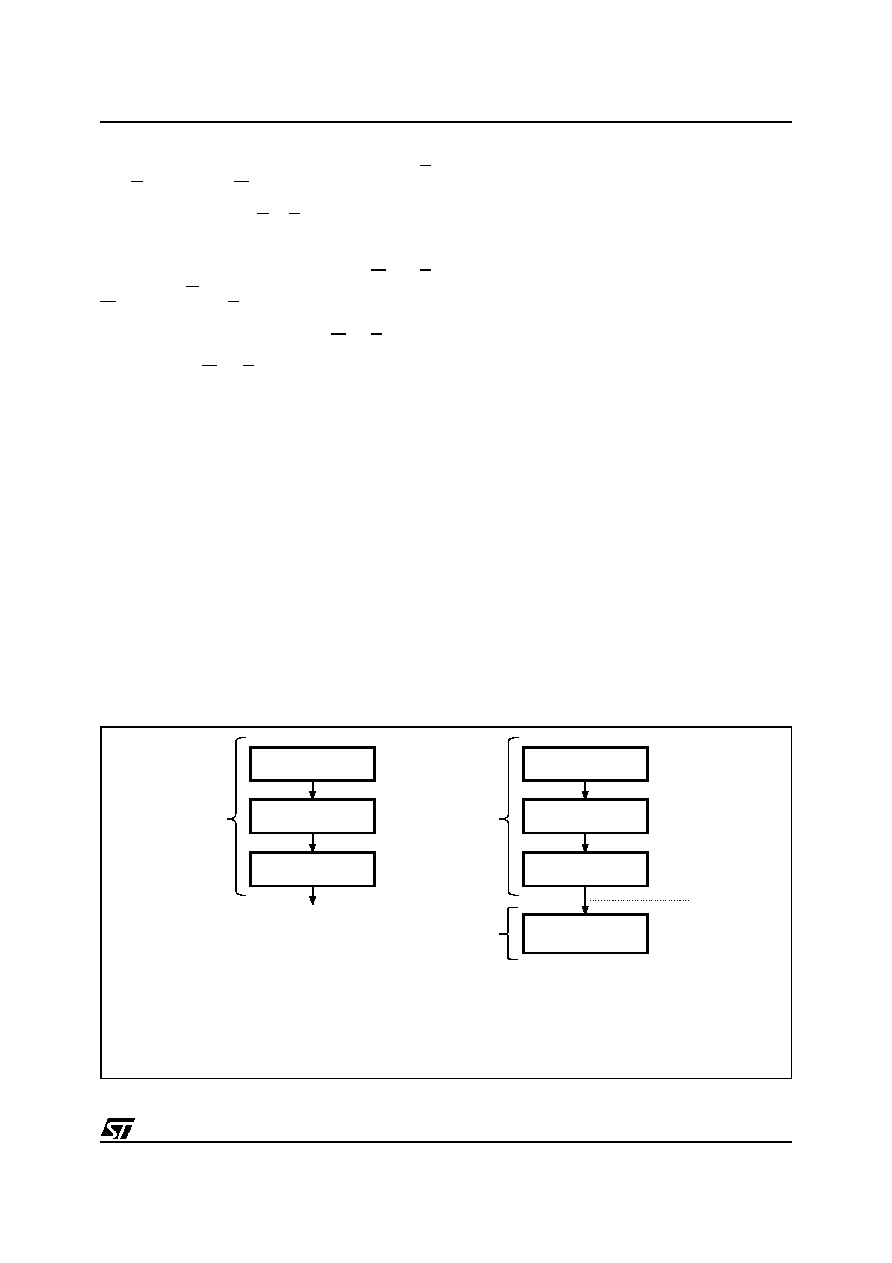
Software Data Protection (SDP)
The device offers a software-controlled write-
protection mechanism that allows the user to
inhibit all write operations to the device. This can
be useful
for protecting
the
memory
from
inadvertent write cycles that may occur during
periods of instability (uncontrolled bus conditions
when excessive noise is detected, or when power
supply levels are outside their specified values).
By
default,
the
device
is
shipped
in
the
"unprotected" state: the memory contents can be
freely changed by the user. Once the Software
Data Protection Mode is enabled, all write
commands are ignored, and have no effect on the
memory contents.
The device remains in this mode until a valid
Software Data Protection disable sequence is
received. The device reverts to its "unprotected"
state.
The status of the Software Data Protection
(enabled or disabled) is represented by a non-
Figure 4. Software Data Protection Enable Algorithm and Memory Write
Note: 1. The most significant address bits (A12 to A6) differ during these specific Page Write operations.
AI01356C
Write AAh in
Address 1555h
Write 55h in
Address 0AAAh
Write A0h in
Address 1555h
SDP is set
Write AAh in
Address 1555h
Write 55h in
Address 0AAAh
Write A0h in
Address 1555h
Page Write
(1 up to 64 bytes)
Write to Memory
When SDP is SET
SDP Enable Algorithm
Page Write
Timing
(see note 1)
Page Write
Timing
(see note 1)
Write
is enabled
Physical
Page Write
Instruction