 | –≠–ª–µ–∫—Ç—Ä–æ–Ω–Ω—ã–π –∫–æ–º–ø–æ–Ω–µ–Ω—Ç: M28F420 | –°–∫–∞—á–∞—Ç—å:  PDF PDF  ZIP ZIP |
AI01130C
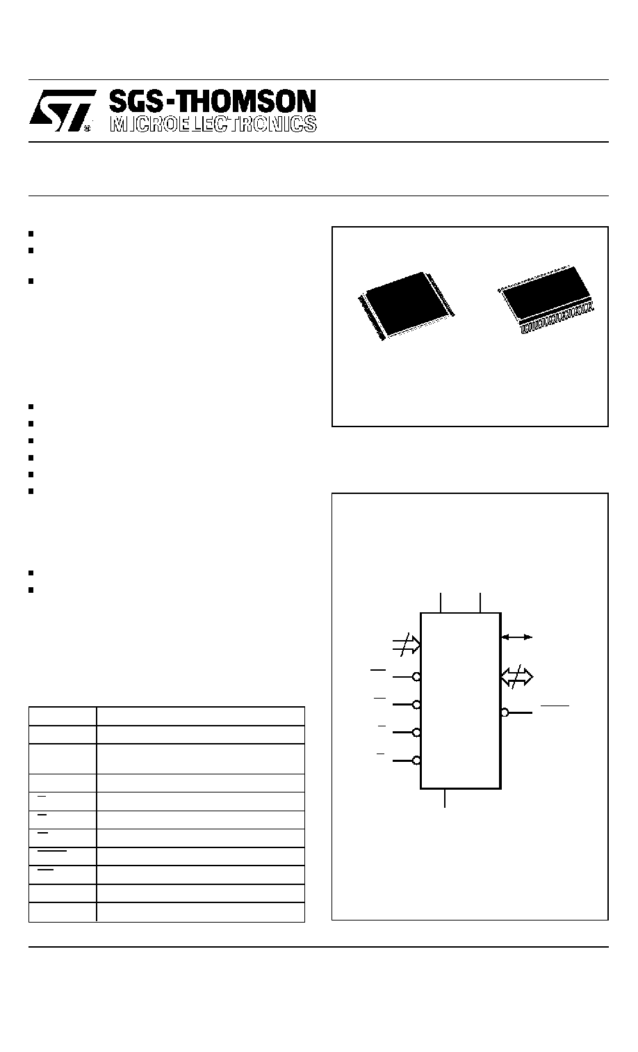
18
A0-A17
W
DQ0-DQ14
VPP
VCC
M28F410
M28F420
G
E
VSS
15
RP
BYTE
DQ15A-1
Figure 1. Logic Diagram
March 1995
M28F410
M28F420
4 Megabit (x8 or x16, Block Erase) FLASH MEMORY
PRELIMINARY DATA
DUAL x8 and x16 ORGANIZATION
SMALL SIZE PLASTIC PACKAGES TSOP56
and SO44
MEMORY ERASE in BLOCKS
≠ One 16K Byte or 8K Word Boot Block (top or
bottom location) with hardware write and
erase protection
≠ Two 8K Byte or 4K Word Key Parameter
Blocks
≠ One 96K Byte or 48K Word Main Block
≠ Three 128K Byte or 64K Word Main Blocks
5V
±
10% SUPPLY VOLTAGE
12V
±
5% PROGRAMMING VOLTAGE
100,000 PROGRAM/ERASE CYCLES
PROGRAM/ERASE CONTROLLER
AUTOMATIC STATIC MODE
LOW POWER CONSUMPTION
≠ 60
A Typical in Standby
≠ 0.2
A Typical in Deep Power Down
≠ 20/25mA Typical Operating Consumption
(Byte/Word)
HIGH SPEED ACCESS TIME: 70ns
EXTENDED TEMPERATURE RANGES
A0-A17
Address Inputs
DQ0-DQ7
Data Input / Outputs
DQ8-
DQ14
Data Input / Outputs
DQ15A-1
Data Input/Output or Address Input
E
Chip Enable
G
Output Enable
W
Write Enable
BYTE
Byte/Word Organization
RP
Reset/Power Down/Boot Block Unlock
V
PP
Program & Erase Supply Voltage
V
CC
Supply Voltage
Table 1. Signal Names
This is preliminary infor mationon a new product now in developmen t or undergoing evaluation. Details are subject to change without notice.
44
1
SO44 (M)
TSOP56 (N)
14 x 20mm
1/38
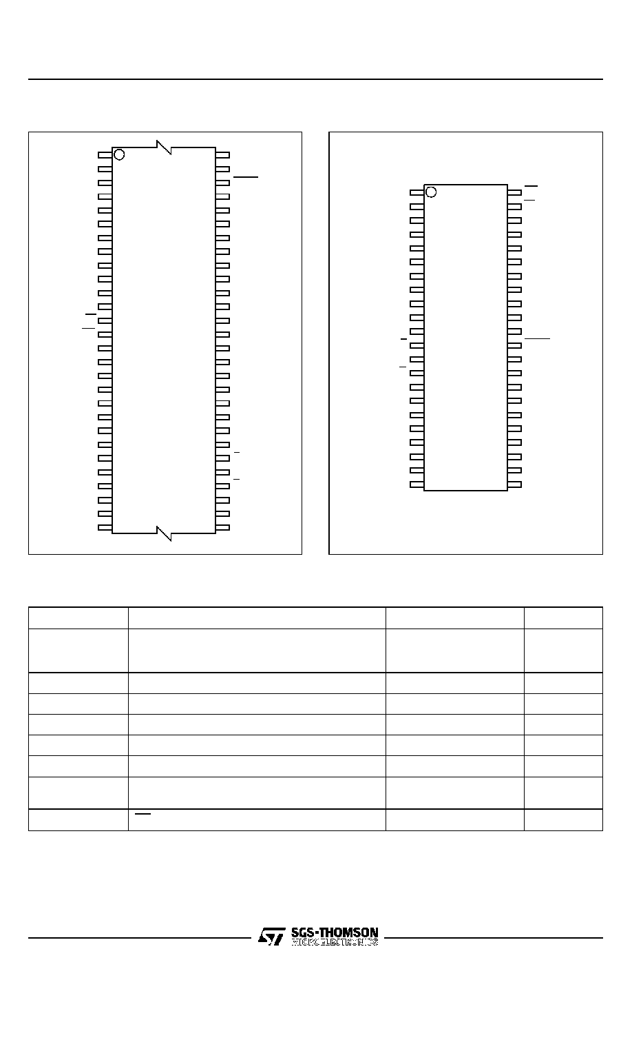
VSS
DQ9
DQ2
DU
NC
E
A3
A2
A8
A16
A15
NC
DQ5
NC
NC
G
BYTE
DQ4
DQ10
DQ3
VCC
VCC
DQ12
NC
W
NC
NC
VPP
RP
AI01132C
M28F410
M28F420
(Normal)
14
1
15
28
29
42
43
56
NC
A13
A14
NC
DQ15A-1
A4
NC
DQ11
DQ0
VSS
A1
A11
A12
A9
A10
DQ14
DQ6
DQ13
DQ7
A6
A17
A7
A5
DQ8
DQ1
A0
NC
Figure 2A. TSOP Pin Connections
Warning: NC = Not Connected, DU = Don't Use
G
DQ0
DQ8
A3
A0
E
VSS
A2
A1
A13
VSS
A14
A15
DQ7
A12
A16
BYTE
DQ15A-1
DQ5
DQ2
DQ3
VCC
DQ11
DQ4
DQ14
A9
W
DU
A4
VPP
RP
A7
AI01133C
M28F410
M28F420
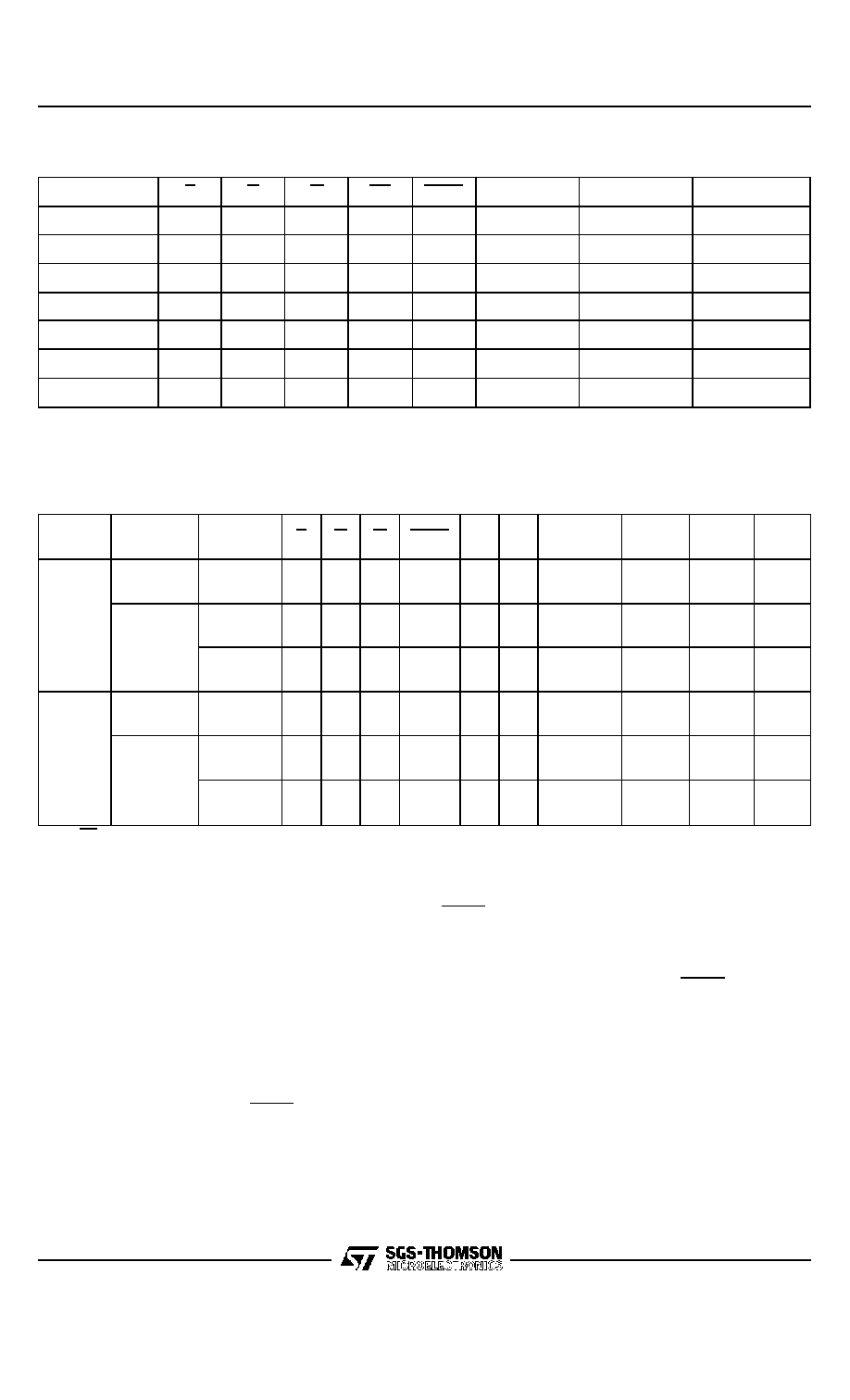
8
2
3
4
5
6
7
9
10
11
12
13
14
15
16
32
31
30
29
28
27
26
25
24
23
22
20
19
18
17
DQ1
DQ9
A6
A5
DQ6
DQ13
44
39
38
37
36
35
34
33
A11
A10
DQ10
21
DQ12
40
43
1
42
41
A17
A8
Figure 2B. SO Pin Connections
Warning: DU = Don't Use
Symbol
Parameter
Value
Unit
T
A
Ambient Operating Temperature
grade 1
grade 3
grade 6
0 to 70
≠40 to 125
≠40 to 85
∞
C
T
BIAS
Temperature Under Bias
≠50 to 125
∞
C
T
STG
Storage Temperature
≠65 to 150
∞
C
V
IO
(2, 3)
Input or Output Voltages
≠0.6 to 7
V
V
CC
Supply Voltage
≠0.6 to 7
V
V
A9
(2)
A9 Voltage
≠0.6 to 13.5
V
V
PP
(2)
Program Supply Voltage, during Erase
or Programming
≠0.6 to 14
V
V
RP
(2)
RP Voltage
≠0.6 to 13.5
V
Notes: 1. Except for the rating "Operating Temperature Range", stresses above those listed in the Table "Absolute Maximum Ratings"
may cause permanent damage to the device. These are stress ratings only and operation of the device at these or any other
conditions above those indicated in the Operating sections of this specification is not implied. Exposure to Absolute Maximum
Rating conditions for extended periods may affect device reliability. Refer also to the SGS-THOMSON SURE Program and other
relevant quality documents.
2. Minimum Voltage may undershoot to ≠2V during transition and for less than 20ns.
3. Maximum DC voltage on I/O is V
CC
+ 0.5V, overshoot to 7V allowed for less than 20ns.
Table 2. Absolute Maximum Ratings
(1)
2/38
M28F410, M28F420
Operation
E
G
W
RP
BYTE
DQ0 - DQ7
DQ8 - DQ14
DQ15A-1
Read Word
V
IL
V
IL
V
IH
V
IH
V
IH
Data Output
Data Output
Data Output
Read Byte
V
IL
V
IL
V
IH
V
IH
V
IL
Data Output
Hi-Z
Address Input
Write Word
V
IL
V
IH
V
IL
V
IH
V
IH
Data Input
Data Input
Data Input
Write Byte
V
IL
V
IH
V
IL
V
IH
V
IL
Data Input
Hi-Z
Address Input
Output Disable
V
IL
V
IH
V
IH
V
IH
X
Hi-Z
Hi-Z
Hi-Z
Standby
V
IH
X
X
V
IH
X
Hi-Z
Hi-Z
Hi-Z
Power Down
X
X
X
V
IL
X
Hi-Z
Hi-Z
Hi-Z
Note: X = V
IL
or V
IH
, V
PP
= V
PPL
or V
PPH
Table 3. Operations
DESCRIPTION
The M28F410 and M28F420 FLASH MEMORIES
are non-volatile memories that may be erased
electrically at the block level and programmed by
byte or word. The interface is directly compatible
with most microprocessors. SO44 and TSOP56
packages are used.
Organization
The organization, as 512K x 8 or 256K x 16, is
selectable by an external BYTE signal. When
BYTE is Low and the x8 organization is selected,
the Data Input/Outputsignal DQ15 acts as Address
line A-1 and selects the lower or upper byte of the
memory word for output on DQ0-DQ7, DQ8-DQ14
remain high impedance. When BYTE is High the
memory uses the Address inputs A0-A17 and the
Data Input/OutputsDQ0-DQ15. Memory control is
provided by Chip Enable, Output Enable and Write
Enable inputs. A Reset/Power Down/Boot block
unlock, tri-level input, places the memory in deep
power down, normal operation or enables pro-
gramming and erasure of the Boot block.
Organi-
sation
Code
Device
E
G
W
BYTE
A0
A9
A1-A8 &
A10-A17
DQ0 -
DQ7
DQ8 -
DQ14
DQ15
A-1
Word-
wide
Manufact.
Code
V
IL
V
IL
V
IH
V
IH
V
IL
V
ID
Don't
Care
20h
00h
0
Device
Code
M28F410
V
IL
V
IL
V
IH
V
IH
V
IH
V
ID
Don't
Care
0F2h
00h
0
M28F420
V
IL
V
IL
V
IH
V
IH
V
IH
V
ID
Don't
Care
0FAh
00h
0
Byte-
wide
Manufact.
Code
V
IL
V
IL
V
IH
V
IL
V
IL
V
ID
Don't
Care
20h
Hi-Z
Don't
Care
Device
Code
M28F410
V
IL
V
IL
V
IH
V
IL
V
IH
V
ID
Don't
Care
0F2h
Hi-Z
Don't
Care
M28F420
V
IL
V
IL
V
IH
V
IL
V
IH
V
ID
Don't
Care
0FAh
Hi-Z
Don't
Care
Note: RP = V
IH
Table 4. Electronic Signature
3/38
M28F410, M28F420

Mne-
monic
Instruction
Cycles
1st Cycle
2nd Cycle
Operation
Address
(1)
Data
(4 )
Operation
Address
Data
RD
Read
Memory
Array
1+
Write
X
0FFh
Read
(2)
Read
Address
Data
RSR
Read
Status
Register
1+
Write
X
70h
Read
(2)
X
Status
Register
RSIG
Read
Electronic
Signature
3
Write
X
90h
Read
(2)
Signature
Adress
(3)
Signature
EE
Erase
2
Write
X
20h
Write
Block
Address
0D0h
PG
Program
2
Write
X
40h or 10h
Write
Address
Data Input
CLRS
Clear
Status
Register
1
Write
X
50h
ES
Erase
Suspend
1
Write
X
0B0h
ER
Erase
Resume
1
Write
X
0D0h
Notes: 1. X = Don't Care.
2. The first cycle of the RD, RSR or RSIG instruction is followed by read operations to read memory array, Status Register
or Electronic Signature codes. Any number of Read cycle can occur after one command cycle.
3. Signature address bit A0=V
IL
will output Manufacturer code. Address bit A0=V
IH
will output Device code. Other address bits are
ignored.
4. When word organization is used, upper byte is don't care for command input.
Table 5. Instructions
Hex Code
Command
00h
Invalid/Reserved
10h
Alternative Program Set-up
20h
Erase Set-up
40h
Program Set-up
50h
Clear Status Register
70h
Read Status Register
90h
Read Electronic Signature
0B0h
Erase Suspend
0D0h
Erase Resume/Erase Confirm
0FFh
Read Array
Table 6. Commands
Blocks
Erasure of the memories is in blocks. There are 7
blocks in the memory address space, one Boot
Block of 16K Bytes or 8K Words, two 'Key Parame-
ter Blocks' of 8K Bytes or 4K Words, one 'Main
Block' of 96K Bytes or 48K Words, and three 'Main
Blocks' of 128KBytes or 64K Words. The M28F410
memory has the Boot Block at the top of the mem-
ory address space (3FFFFh) and the M28F420
locates the Boot Block starting at the bottom
(00000h). Erasure of each block takes typically 1
second and each block can be programmed and
erased over 100,000 cycles.
The Boot Block is hardware protected from acci-
dental programming or erasure depending on the
RP signal. Program/Erase commands in the Boot
Block are executed only when RP is at 12V. Block
erasure may be suspended while data is read from
other blocks of the memory, then resumed.
Bus Operations
Six operationscan be performed by the appropriate
bus cycles, Read Byte or Word from the Array,
Read Electronic Signature, Output Disable,
Standby, Power Down and Write the Command of
an Instruction.
Command Interface
Commands can be written to a Command Interface
(C.I.) latch to perform read, programming, erasure
and to monitor the memory's status. When power
4/38
M28F410, M28F420
Mne-
monic
Bit
Name
Logic
Level
Definition
Note
P/ECS
7
P/E.C. Status
'1'
Ready
Indicates the P/E.C. status, check during Program
or Erase, and on completion before checking bits
b4 or b5 for Program or Erase Success
'0'
Busy
ESS
6
Erase
Suspend
Status
'1'
Suspended
On an Erase Suspend instruction P/ECS and
ESS bits are set to '1'. ESS bit remains '1' until an
Erase Resume instruction is given.
'0'
In progress or
Completed
ES
5
Erase Status
'1'
Erase Error
ES bit is set to '1' if P/E.C. has applied the
maximum number of erase pulses to the block
without achieving an erase verify.
'0'
Erase Success
PS
4
Program
Status
'1'
Program Error
PS bit set to '1' if the P/E.C. has failed to program
a byte or word.
'0'
Program
Success
VPPS
3
V
PP
Status
'1'
V
PP
Low, Abort
VPPS bit is set if the V
PP
voltage is below
V
PPH
(min) when a Program or Erase instruction
has been executed.
'0'
V
PP
OK
2
Reserved
1
Reserved
0
Reserved
Notes: Logic level '1' is High, '0' is Low.
Table 7. Status Register
is first applied, on exit from power down or if V
CC
falls below V
LKO
, the command interface is reset to
Read Memory Array.
Instructions and Commands
Eight Instructions are defined to perform Read
Memory Array, Read Status Register, Read Elec-
tronic Signature, Erase, Program, Clear Status
Register, Erase Suspend and Erase Resume. An
internal Program/EraseController (P/E.C.) handles
all timing and verification of the Program and Erase
instructions and provides status bits to indicate its
operation and exit status. Instructions are com-
posed of a first command write operation followed
by either second command write, to confirm the
commands for programming or erase, or a read
operation to read data from the array, the Electronic
Signature or the Status Register.
For added data protection, the instructions for byte
or word program and block erase consist of two
commands that are written to the memory and
which start the automatic P/E.C. operation. Byte or
word programming takes typically 9
s, block erase
typically 1 second. Erasure of a memory block may
be suspended in order to read data from another
block and then resumed. A Status Register may be
read at any time, including during the programming
or erase cycles, to monitor the progress of the
operation.
Power Saving
The M28F410 and M28F420 have a number of
power saving features. A CMOS standby mode is
entered when the Chip Enable E and the Re-
set/Power Down (RP) signals are at V
CC
, when the
supply current drops to typically 60
A. A deep
power down mode is enabled when the Re-
set/Power Down (RP) signal is at V
SS
, when the
supply current drops to typically 0.2
A. The time
required to awake from the deep power down mode
is 300ns maximum, with instructions to the C.I.
recognised after only 210ns.
5/38
M28F410, M28F420