1/11
June 2004
M28R400CT-KGD
M28R400CB-KGD
Known Good Die
4 Mbit (256Kb x16, Boot Block) 1.8V Supply Flash Memory
FEATURES SUMMARY
SUPPLY VOLTAGE
≠
V
DD
= 1.65V to 2.2V Core Power Supply
≠
V
DDQ
= 1.65V to 2.2V for Input/Output
≠
V
PP
= 12V for fast Program (optional)
ACCESS TIME: 100ns
PROGRAMMING TIME
≠
10µs typical
≠
Double Word Programming Option
COMMON FLASH INTERFACE
≠
64 bit Security Code
MEMORY BLOCKS
≠
Parameter Blocks (Top or Bottom
location)
≠
Main Blocks
BLOCK LOCKING
≠
All blocks locked at Power Up
≠
Any combination of blocks can be locked
≠
WP for Block Lock-Down
SECURITY
≠
64 bit user Programmable OTP cells
≠
64 bit unique device identifier
≠
One Parameter Block Permanently
Lockable
AUTOMATIC STAND-BY MODE
PROGRAM and ERASE SUSPEND
100,000 PROGRAM/ERASE CYCLES per
BLOCK
ELECTRONIC SIGNATURE
≠
Manufacturer Code: 20h
≠
Top Device Code, M28R400CT: 882Ah
≠
Bottom Device Code, M28R400CB:
882Bh
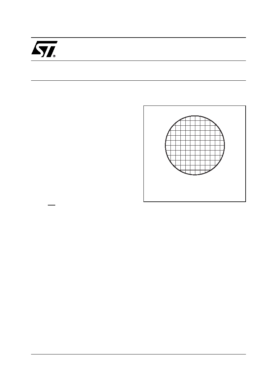
Figure 1. Delivery Form
Wafer

M28R400CT-KGD, M28R400CB-KGD
2/11
TABLE OF CONTENTS
FEATURES SUMMARY . . . . . . . . . . . . . . . . . . . . . . . . . . . . . . . . . . . . . . . . . . . . . . . . . . . . . . . . . . . . . 1
Figure 1. Delivery Form . . . . . . . . . . . . . . . . . . . . . . . . . . . . . . . . . . . . . . . . . . . . . . . . . . . . . . . . . . 1
SUMMARY DESCRIPTION. . . . . . . . . . . . . . . . . . . . . . . . . . . . . . . . . . . . . . . . . . . . . . . . . . . . . . . . . . . 3
Figure 2. Logic Diagram . . . . . . . . . . . . . . . . . . . . . . . . . . . . . . . . . . . . . . . . . . . . . . . . . . . . . . . . . . 3
Table 1. Signal Names . . . . . . . . . . . . . . . . . . . . . . . . . . . . . . . . . . . . . . . . . . . . . . . . . . . . . . . . . . 3
FUNCTIONAL SPECIFICATION. . . . . . . . . . . . . . . . . . . . . . . . . . . . . . . . . . . . . . . . . . . . . . . . . . . . . . . 4
Table 2. Product Specification . . . . . . . . . . . . . . . . . . . . . . . . . . . . . . . . . . . . . . . . . . . . . . . . . . . . . 4
Table 3. Operating Conditions . . . . . . . . . . . . . . . . . . . . . . . . . . . . . . . . . . . . . . . . . . . . . . . . . . . . . 4
Table 4. Read AC Characteristics . . . . . . . . . . . . . . . . . . . . . . . . . . . . . . . . . . . . . . . . . . . . . . . . . . 4
Table 5. Write AC Characteristics . . . . . . . . . . . . . . . . . . . . . . . . . . . . . . . . . . . . . . . . . . . . . . . . . . 4
Table 6. Physical Specification . . . . . . . . . . . . . . . . . . . . . . . . . . . . . . . . . . . . . . . . . . . . . . . . . . . . 4
Table 7. Manufacturing Information . . . . . . . . . . . . . . . . . . . . . . . . . . . . . . . . . . . . . . . . . . . . . . . . . 4
DIE SPECIFICATIONS . . . . . . . . . . . . . . . . . . . . . . . . . . . . . . . . . . . . . . . . . . . . . . . . . . . . . . . . . . . . . . 5
Figure 3. Die Photograph and Pad Location. . . . . . . . . . . . . . . . . . . . . . . . . . . . . . . . . . . . . . . . . . . 5
Figure 4. Wafer/Die Orientation . . . . . . . . . . . . . . . . . . . . . . . . . . . . . . . . . . . . . . . . . . . . . . . . . . . . 5
Table 8. Pad Extraction . . . . . . . . . . . . . . . . . . . . . . . . . . . . . . . . . . . . . . . . . . . . . . . . . . . . . . . . . . 6
PRODUCT TEST FLOW . . . . . . . . . . . . . . . . . . . . . . . . . . . . . . . . . . . . . . . . . . . . . . . . . . . . . . . . . . . . . 7
Figure 5. Product Test Flow . . . . . . . . . . . . . . . . . . . . . . . . . . . . . . . . . . . . . . . . . . . . . . . . . . . . . . . 7
HANDLING INSTRUCTIONS . . . . . . . . . . . . . . . . . . . . . . . . . . . . . . . . . . . . . . . . . . . . . . . . . . . . . . . . . 8
Processing . . . . . . . . . . . . . . . . . . . . . . . . . . . . . . . . . . . . . . . . . . . . . . . . . . . . . . . . . . . . . . . . . . . . 8
Storage . . . . . . . . . . . . . . . . . . . . . . . . . . . . . . . . . . . . . . . . . . . . . . . . . . . . . . . . . . . . . . . . . . . . . . . 8
PART NUMBERING . . . . . . . . . . . . . . . . . . . . . . . . . . . . . . . . . . . . . . . . . . . . . . . . . . . . . . . . . . . . . . . . 9
Table 9. Ordering Information Scheme . . . . . . . . . . . . . . . . . . . . . . . . . . . . . . . . . . . . . . . . . . . . . . 9
REVISION HISTORY . . . . . . . . . . . . . . . . . . . . . . . . . . . . . . . . . . . . . . . . . . . . . . . . . . . . . . . . . . . . . . . 10
Table 10. Document Revision History . . . . . . . . . . . . . . . . . . . . . . . . . . . . . . . . . . . . . . . . . . . . . . . 10
3/11
M28R400CT-KGD, M28R400CB-KGD
SUMMARY DESCRIPTION
The M28R400C are available as Known Good
Dice.
STMicroelectronics defines Known Good Dice as
standard products offered as dice and tested for
functionality and speed. ST's Known Good Die
products are as reliable and of the same quality as
products delivered in packages.
This datasheet should be read in conjunction with
the full M28R400C datasheet.
The M28R400C is a 4 Mbit (256Kbit x 16) non-vol-
atile Flash memory that can be erased electrically
at the block level and programmed in-system on a
Word-by-Word basis. These operations can be
performed using a single low voltage (1.65 to
2.2V) supply. V
DDQ
allows to drive the I/O pin
down to 1.65V. An optional 12V V
PP
power supply
is provided to speed up customer programming.
The device features an asymmetrical blocked ar-
chitecture. The M28R400C has an array of 15
blocks: 8 Parameter Blocks of 4 KWord and 7
Main Blocks of 32 KWord. M28R400CT has the
Parameter Blocks at the top of the memory ad-
dress space while the M28R400CB locates the
Parameter Blocks starting from the bottom.
The M28R400C features an instant, individual
block locking scheme that allows any block to be
locked or unlocked with no latency, enabling in-
stant code and data protection. All blocks have
three levels of protection. They can be locked and
locked-down individually preventing any acciden-
tal programming or erasure. There is an additional
hardware protection against program and block
erase. When V
PP
V
PPLK
all blocks are protected
against program or block erase. All blocks are
locked at power-up.
Each block can be erased separately. Erase can
be suspended in order to perform either read or
program in any other block and then resumed.
Program can be suspended to read data in any
other block and then resumed. Each block can be
programmed and erased over 100,000 cycles.
The device includes a 128 bit Protection Register
and a Security Block to increase the protection of
a system design. The Protection Register is divid-
ed into two 64 bit segments, the first one contains
a unique device number written by ST, while the
second one is one-time-programmable by the us-
er. The user programmable segment can be per-
manently protected. The Security Block,
parameter block 0, can be permanently protected
by the user.
Program and Erase commands are written to the
Command Interface of the memory. An on-chip
Program/Erase Controller takes care of the tim-
ings necessary for program and erase operations.
The end of a program or erase operation can be
detected and any error conditions identified. The
command set required to control the memory is
consistent with JEDEC standards.
The M28R400C are supplied with all the bits
erased (set to `1')
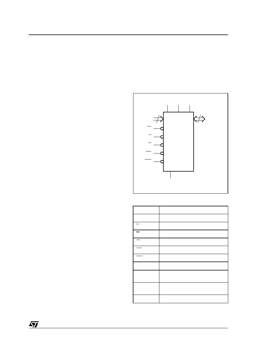
Figure 2. Logic Diagram
Table 1. Signal Names
A0-A17
Address Inputs
DQ0-DQ15
Data Input/Output
E
Chip Enable
G
Output Enable
W
Write Enable
RP
Reset
WP
Write Protect
V
DD
Core Power Supply
V
DDQ
Power Supply for
Input/Output
V
PP
Optional Supply Voltage for
Fast Program & Erase
V
SS
Ground
AI04392
18
A0-A17
W
DQ0-DQ15
VDD
M28R400CT
M28R400CB
E
VSS
16
G
RP
WP
VDDQ VPP
M28R400CT-KGD, M28R400CB-KGD
4/11
FUNCTIONAL SPECIFICATION
Refer to the M28R400C (document number 7653
on the ST Internet web site http://www.st.com) for
full functional and electrical specifications of the
product.
Table 2.
and
Table 3.
give the main product spec-
ification and operating conditions while
Table 4.
and
Table 5.
summarize the Read and Write AC
parameters which differ from those given in the
M28R400C datasheet.
See
Table 6.
and
Table 7.
for details of the die's
physical specification and manufacturing.
Table 2. Product Specification
Table 3. Operating Conditions
Table 4. Read AC Characteristics
Table 5. Write AC Characteristics
Table 6. Physical Specification
Table 7. Manufacturing Information
Product Root Part Number
M28R400CT
M28R400CB
Speed Option
100ns
Delivery Form
Inked or mapped dice on
whole unsawn wafer
Supply Voltage
V
DD
= V
DDQ
= 1.65V to 2.2V
Junction Temperature
Under Bias
TJ (max) = 125∞C
Operating Temperature
-
40∞C to +85∞C
Symbol
Description
Value
Unit
t
AVAV
Address Valid to Next
Address Valid (min)
100
ns
t
AVQV
Address Valid to Output
Valid (max)
100
ns
t
EHQZ
Chip Enable High to
Output Hi-Z (max)
25
ns
t
ELQV
Chip Enable Low to
Output Valid (max)
100
ns
t
GHQZ
Output Enable High to
Output Hi-Z (max)
25
ns
t
GLQV
Output Enable Low to
Output Valid (max)
30
ns
Symbol
Description
Value
Unit
t
AVAV
Address Valid to Next
Address Valid (min)
100
ns
t
ELQV
Chip Enable Low to
Output Valid (max)
100
ns
Die Dimensions, X by Y
(with scribe line)
141.024 mils x 98.504 mils
3.582mm x 2.502mm
Die Dimensions, X by Y
(without scribe line)
137.008mils x 94.488mils
3.480mm x 2.400mm
Die Thickness
9.84 mils
725µm
Bond Pad Size
3.56 mils x 3.56 mils
90.4µm x 90.4µm
Pad Area Free of
Passivation
12.67 mils≤
8172µm≤
Pad per Die
46
Bond Pad Metallization
AlCU, TiN
Die Backside
No Metal
May be grounded
Passivation
USG, Si
3
N
4
Manufacturing Location -
Die Revision
Catania (M5 fab), Italy ≠ V2
Manufacturing Location -
Die Revision
Agrate (R2 fab), Italy ≠ V1
Wafer Sort and Test
Location
Agrate and Catania, Italy
Manufacturing ID
SA2B9AZ
Preparation for Shipment
Agrate and Catania, Italy
Fabrication Process
0.18µm technology
5/11
M28R400CT-KGD, M28R400CB-KGD
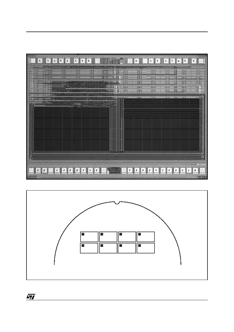
DIE SPECIFICATIONS
Figure 3. Die Photograph and Pad Location
Figure 4. Wafer/Die Orientation
21
22
34
35
46
1
10
11
LOGO
LOGO
LOGO
LOGO
LOGO
LOGO
LOGO
LOGO
LOGO
AI08416
WAFER FRONT SIDE