 | –≠–ª–µ–∫—Ç—Ä–æ–Ω–Ω—ã–π –∫–æ–º–ø–æ–Ω–µ–Ω—Ç: M28W160BB | –°–∫–∞—á–∞—Ç—å:  PDF PDF  ZIP ZIP |

1/39
May 2000
M28W160BT
M28W160BB
16 Mbit (1Mb x16, Boot Block) Low Voltage Flash Memory
s
SUPPLY VOLTAGE
≠ V
DD
= 2.7V to 3.6V: for Program, Erase and
Read
≠ V
DDQ
= 1.65V or 2.7V: Input/Output option
≠ V
PP
= 12V: optional Supply Voltage for fast
Program
s
ACCESS TIME
≠ 2.7V to 3.6V: 90ns
≠ 2.7V to 3.6V: 100ns
s
PROGRAMMING TIME:
≠ 10µs typical
≠ Double Word Programming Option
s
PROGRAM/ERASE CONTROLLER (P/E.C.)
s
COMMON FLASH INTERFACE
≠ 64 bit Security Code
s
MEMORY BLOCKS
≠ Parameter Blocks (Top or Bottom location)
≠ Main Blocks
s
BLOCK PROTECTION on TWO PARAMETER
BLOCKS
≠ WP for Block Protection
s
AUTOMATIC STAND-BY MODE
s
PROGRAM and ERASE SUSPEND
s
100,000 PROGRAM/ERASE CYCLES per
BLOCK
s
20 YEARS of DATA RETENTION
≠ Defectivity below 1ppm/year
s
ELECTRONIC SIGNATURE
≠ Manufacturer Code: 20h
≠ Top Device Code, M28W160BT: 90h
≠ Bottom Device Code, M28W160BB: 91h
Figure 1. Logic Diagram
AI02628
20
A0-A19
W
DQ0-DQ15
VDD
M28W160BT
M28W160BB
E
VSS
16
G
RP
WP
VDDQ VPP
TSOP48 (N)
12 x 20mm
µBGA46 (GB)
8 x 6 solder balls
µ
BGA
M28W160BT, M28W160BB
2/39
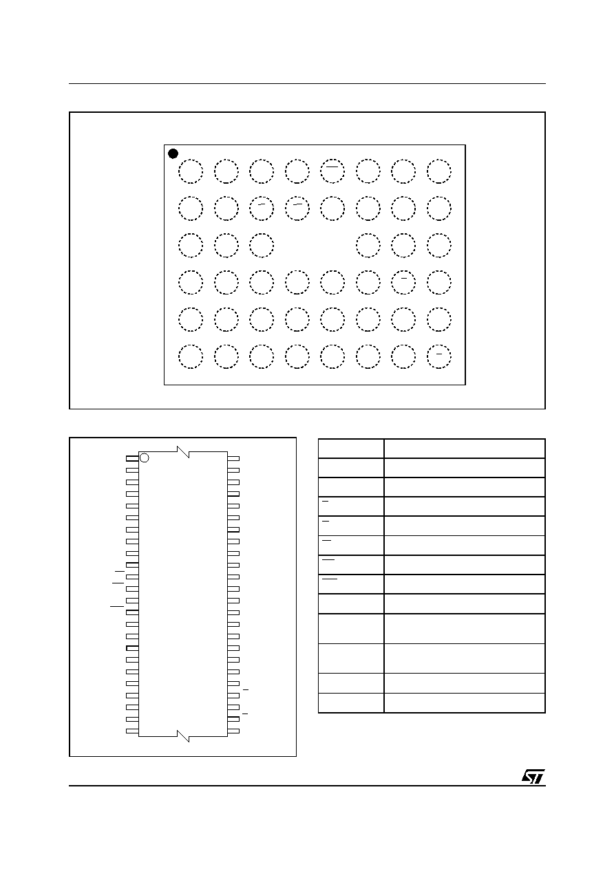
Figure 2. µBGA Connections (Top view through package)
AI02629
C
B
A
8
7
6
5
4
3
2
1
E
D
F
A4
A7
VPP
A8
A11
A13
A0
E
DQ8
DQ5
DQ14
A16
VSS
DQ0
DQ9
DQ3
DQ6
DQ15
VDDQ
DQ1
DQ10
VDD
DQ7
VSS
DQ2
A2
A5
A17
W
A10
A14
A1
A3
A6
A9
A12
A15
RP
A18
DQ4
DQ13
G
DQ12
DQ11
WP
A19
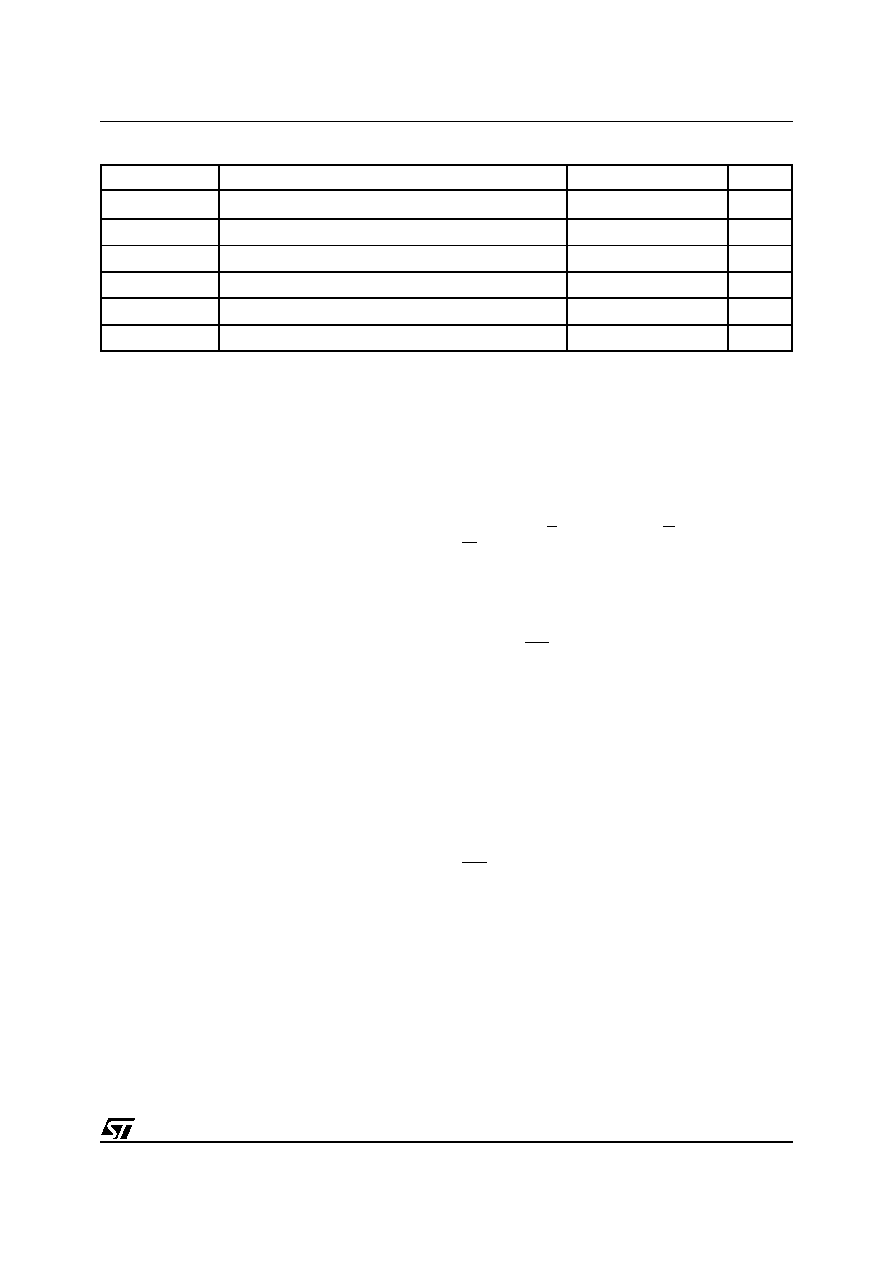
Figure 3. TSOP Connections
DQ3
DQ9
DQ2
A6
DQ0
W
A3
NC
DQ6
A8
A9
DQ13
A17
A10
DQ14
A2
DQ12
DQ10
DQ15
VDD
DQ4
DQ5
A7
DQ7
VPP
WP
AI02630
M28W160BT
M28W160BB
12
1
13
24
25
36
37
48
DQ8
NC
A19
A1
A18
A4
A5
DQ1
DQ11
G
A12
A13
A16
A11
VDDQ
A15
A14
VSS
E
A0
RP
VSS
Table 1. Signal Names
A0-A19
Address Inputs
DQ0-DQ7
Data Input/Output, Command Inputs
DQ8-DQ15
Data Input/Output
E
Chip Enable
G
Output Enable
W
Write Enable
RP
Reset
WP
Write Protect
V
DD
Supply Voltage
V
DDQ
Power Supply for
Input/Output Buffers
V
PP
Optional Supply Voltage for
Fast Program & Erase
V
SS
Ground
NC
Not Connected Internally
3/39
M28W160BT, M28W160BB
DESCRIPTION
The M28W160B is a 16 Mbit non-volatile Flash
memory that can be erased electrically at the block
level and programmed in-system on a Word-by-
Word basis. The device is offered in the TSOP48
(10 x 20mm) and the µBGA46, 0.75mm ball pitch
packages. When shipped, all bits of the
M28W160B are in the `1' state.
The array matrix organisation allows each block to
be erased and reprogrammed without affecting
other blocks. Each block can be programmed and
erased over 100,000 cycles. V
DDQ
allows to drive
the I/O pin down to 1.65V. An optional 12V V
PP
power supply is provided to speed up the program
phase at customer production line environment.
An internal Command Interface (C.I.) decodes the
instructions to access/modify the memory content.
The Program/Erase Controller (P/E.C.) automati-
cally executes the algorithms taking care of the
timings necessary for program and erase opera-
tions. Verification is performed too, unburdening
the microcontroller, while the Status Register
tracks the status of the operation.
The following instructions are executed by the
M28W160B: Read Array, Read Electronic Signa-
ture, Read Status Register, Clear Status Register,
Program, Double Word Program, Block Erase,
Program/Erase Suspend, Program/Erase Re-
sume and CFI Query.
Organisation
The M28W160B is organised as 1 Mbit by 16 bits.
A0-A19 are the address lines; DQ0-DQ15 are the
Data Input/Output. Memory control is provided by
Chip Enable E, Output Enable G and Write Enable
W inputs. The Program and Erase operations are
managed automatically by the P/E.C. Block pro-
tection against Program or Erase provides addi-
tional data security.
The upper two (or lower two) parameter blocks
can be protected to secure the code content of the
memory. WP controls protection and unprotection
operations.
Memory Blocks
The device features an asymmetrical blocked ar-
chitecture. The M28W160B has an array of 39
blocks: 8 Parameter Blocks of 4 KWord and 31
Main Blocks of 32 KWord. M28W160BT has the
Parameter Blocks at the top of the memory ad-
dress space while the M28W160BB locates the
Parameter Blocks starting from the bottom. The
memory maps are shown in Tables 3 and 4.
The two upper parameter block can be protected
from accidental programming or erasure using
WP. Each block can be erased separately. Erase
can be suspended in order to perform either read
or program in any other block and then resumed.
Program can be suspended to read data in any
other block and then resumed.
Table 2. Absolute Maximum Ratings
(1)
Note: 1. Except for the rating "Operating Temperature Range", stresses above those listed in the Table "Absolute Maximum Ratings" may
cause permanent damage to the device. These are stress ratings only and operation of the device at these or any other conditions
above those indicated in the Operating sections of this specification is not implied. Exposure to Absolute Maximum Rating condi-
tions for extended periods may affect device reliability. Refer also to the STMicroelectronics SURE Program and other relevant qual-
ity documents.
2. Depends on range.
Symbol
Parameter
Value
Unit
T
A
Ambient Operating Temperature
(2)
≠40 to 85
∞C
T
BIAS
Temperature Under Bias
≠40 to 125
∞C
T
STG
Storage Temperature
≠55 to 155
∞C
V
IO
Input or Output Voltage
≠0.6 to V
DDQ
+0.6
V
V
DD
, V
DDQ
Supply Voltage
≠0.6 to 4.1
V
V
PP
Program Voltage
≠0.6 to 13
V
M28W160BT, M28W160BB
4/39
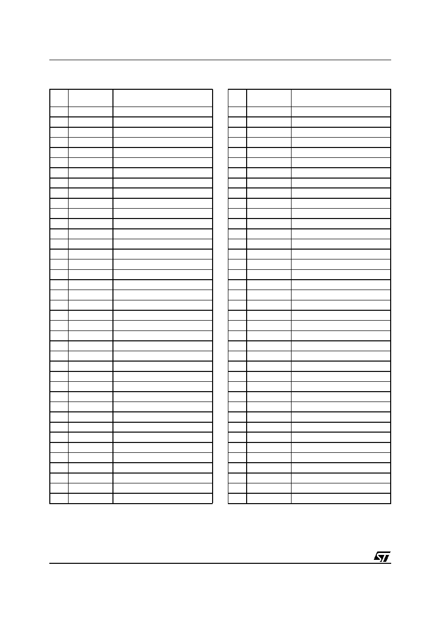
Table 3. Top Boot Block Addresses,
M28W160BT
#
Size
(KWord)
Address Range
38
4
FF000-FFFFF
37
4
FE000-FEFFF
36
4
FD000-FDFFF
35
4
FC000-FCFFF
34
4
FB000-FBFFF
33
4
FA000-FAFFF
32
4
F9000-F9FFF
31
4
F8000-F8FFF
30
32
F0000-F7FFF
29
32
E8000-EFFFF
28
32
E0000-E7FFF
27
32
D8000-DFFFF
26
32
D0000-D7FFF
25
32
C8000-CFFFF
24
32
C0000-C7FFF
23
32
B8000-BFFFF
22
32
B0000-B7FFF
21
32
A8000-AFFFF
20
32
A0000-A7FFF
19
32
98000-9FFFF
18
32
90000-97FFF
17
32
88000-8FFFF
16
32
80000-87FFF
15
32
78000-7FFFF
14
32
70000-77FFF
13
32
68000-6FFFF
12
32
60000-67FFF
11
32
58000-5FFFF
10
32
50000-57FFF
9
32
48000-4FFFF
8
32
40000-47FFF
7
32
38000-3FFFF
6
32
30000-37FFF
5
32
28000-2FFFF
4
32
20000-27FFF
3
32
18000-1FFFF
2
32
10000-17FFF
1
32
08000-0FFFF
0
32
00000-07FFF
Table 4. Bottom Boot Block Addresses,
M28W160BB
#
Size
(KWord)
Address Range
38
32
F8000-FFFFF
37
32
F0000-F7FFF
36
32
E8000-EFFFF
35
32
E0000-E7FFF
34
32
D8000-DFFFF
33
32
D0000-D7FFF
32
32
C8000-CFFFF
31
32
C0000-C7FFF
30
32
B8000-BFFFF
29
32
B0000-B7FFF
28
32
A8000-AFFFF
27
32
A0000-A7FFF
26
32
98000-9FFFF
25
32
90000-97FFF
24
32
88000-8FFFF
23
32
80000-87FFF
22
32
78000-7FFFF
21
32
70000-77FFF
20
32
68000-6FFFF
19
32
60000-67FFF
18
32
58000-5FFFF
17
32
50000-57FFF
16
32
48000-4FFFF
15
32
40000-47FFF
14
32
38000-3FFFF
13
32
30000-37FFF
12
32
28000-2FFFF
11
32
20000-27FFF
10
32
18000-1FFFF
9
32
10000-17FFF
8
32
08000-0FFFF
7
4
07000-07FFF
6
4
06000-06FFF
5
4
05000-05FFF
4
4
04000-04FFF
3
4
03000-03FFF
2
4
02000-02FFF
1
4
01000-01FFF
0
4
00000-00FFF

5/39
M28W160BT, M28W160BB
SIGNAL DESCRIPTIONS
See Figure 1 and Table 1.
Address Inputs (A0-A19). The address signals
are inputs driven with CMOS voltage levels. They
are latched during a write operation.
Data Input/Output (DQ0-DQ15). The data in-
puts, a word to be programmed or a command to
the C.I., are latched on the Chip Enable E or Write
Enable W rising edge, whichever occurs first. The
data output from the memory Array, the Electronic
Signature or Status Register is valid when Chip
Enable E and Output Enable G are active. The
output is high impedance when the chip is dese-
lected, the outputs are disabled or RP is tied to V
IL
.
Commands are issued on DQ0-DQ7.
Chip Enable (E). The Chip Enable input acti-
vates the memory control logic, input buffers, de-
coders and sense amplifiers. E at V
IH
deselects
the memory and reduces the power consumption
to the stand-by level. E can also be used to control
writing to the command register and to the memo-
ry array, while W remains at V
IL
.
Output Enable (G). The Output Enable controls
the data Input/Output buffers.
Write Enable (W). This input controls writing to
the Command Register, Input Address and Data
latches.
Write Protect (WP). Write Protect is an input to
protect or unprotect the two lockable parameter
blocks. When WP is at V
IL
, the lockable blocks are
protected. Program or erase operations are not
achievable. When WP is at V
IH
, the lockable
blocks are unprotected and they can be pro-
grammed or erased (refer to Table 9).
Reset Input (RP). The RP input provides hard-
ware reset of the memory. When RP is at V
IL
, the
memory is in reset mode: the outputs are put to
High-Z and the current consumption is minimised.
When RP is at V
IH
, the device is in normal opera-
tion. Exiting reset mode the device enters read ar-
ray mode.
V
DD
Supply Voltage (2.7V to 3.6V). V
DD
pro-
vides the power supply to the internal core of the
memory device. It is the main power supply for all
operations (Read, Program and Erase). It ranges
from 2.7V to 3.6V.
V
DDQ
Supply Voltage (1.65V to V
DD
). V
DDQ
provides the power supply to the I/O pins and en-
ables all Outputs to be powered independently
from V
DD
. V
DDQ
can be tied to V
DD
or it can use a
separate supply. It can be powered either from
1.65V to 2.2V or from 2.7V to 3.6V.
V
PP
Program Supply Voltage (12V). V
PP
is
both a control input and a power supply pin. The
two functions are selected by the voltage range
applied to the pin.
If V
PP
is kept in a low voltage range (0V to 3.6V)
V
PP
is seen as a control input. In this case a volt-
age lower than V
PPLK
gives an absolute protection
against program or erase, while V
PP
> V
PP1
en-
ables these functions. V
PP
value is only sampled
at the beginning of a program or erase; a change
in its value after the operation has been started
does not have any effect and program or erase are
carried on regularly.
If V
PP
is used in the range 11.4V to 12.6V acts as
a power supply pin. In this condition V
PP
value
must be stable until P/E algorithm is completed
(see Table 22 and 23).
V
SS
Ground. V
SS
is the reference for all the volt-
age measurements.