 | –≠–ª–µ–∫—Ç—Ä–æ–Ω–Ω—ã–π –∫–æ–º–ø–æ–Ω–µ–Ω—Ç: M28W320CB | –°–∫–∞—á–∞—Ç—å:  PDF PDF  ZIP ZIP |

1/42
PRELIMINARY DATA
May 2000
This is preliminary information on a new product now in development or undergoing evaluation. Details are subject to change without notice.
M28W320CT
M28W320CB
32 Mbit (2Mb x16, Boot Block) Low Voltage Flash Memory
s
SUPPLY VOLTAGE
≠ V
DD
= 2.7V to 3.6V: for Program, Erase and
Read
≠ V
DDQ
= 1.65V or 2.7V: Input/Output option
≠ V
PP
= 12V: optional Supply Voltage for fast
Program
s
ACCESS TIME
≠ 2.7V to 3.6V: 90ns
≠ 2.7V to 3.6V: 100ns
s
PROGRAMMING TIME:
≠ 10
µ
s typical
≠ Double Word Programming Option
s
PROGRAM/ERASE CONTROLLER (P/E.C.)
s
COMMON FLASH INTERFACE
s
MEMORY BLOCKS
≠ Parameter Blocks (Top or Bottom location)
≠ Main Blocks
s
BLOCK PROTECTION UNPROTECTION
≠ All Blocks protected at Power Up
≠ Any combination of blocks can be protected
≠ WP for block locking
s
SECURITY
≠ 64-bit user Programmable OTP cells
≠ 64-bit unique device identifier
≠ One Parameter Block Permanently Lockable
s
AUTOMATIC STAND-BY MODE
s
PROGRAM and ERASE SUSPEND
s
100,000 PROGRAM/ERASE CYCLES per
BLOCK
s
20 YEARS of DATA RETENTION
≠ Defectivity below 1ppm/year
s
ELECTRONIC SIGNATURE
≠ Manufacturer Code: 20h
≠ Top Device Code, M28W320CT: 88BAh
≠ Bottom Device Code, M28W320CB: 88BBh
Figure 1. Logic Diagram
AI03521
21
A0-A20
W
DQ0-DQ15
VDD
M28W320CT
M28W320CB
E
VSS
16
G
RP
WP
VDDQ VPP
TSOP48 (N)
12 x 20mm
µ
BGA47 (GB)
8 x 6 solder balls
µ
BGA

M28W320CT, M28W320CB
2/42
Figure 2.
µ
BGA Connections (Top view through package)
AI02686
C
B
A
8
7
6
5
4
3
2
1
E
D
F
A4
A7
VPP
A8
A11
A13
A0
E
DQ8
DQ5
DQ14
A16
VSS
DQ0
DQ9
DQ3
DQ6
DQ15
VDDQ
DQ1
DQ10
VDD
DQ7
VSS
DQ2
A2
A5
A17
W
A10
A14
A1
A3
A6
A9
A12
A15
RP
A18
DQ4
DQ13
G
DQ12
DQ11
WP
A19
A20
Figure 3. TSOP Connections
DQ3
DQ9
DQ2
A6
DQ0
W
A3
NC
DQ6
A8
A9
DQ13
A17
A10
DQ14
A2
DQ12
DQ10
DQ15
VDD
DQ4
DQ5
A7
DQ7
VPP
WP
AI03522
M28W320CT
M28W320CB
12
1
13
24
25
36
37
48
DQ8
A20
A19
A1
A18
A4
A5
DQ1
DQ11
G
A12
A13
A16
A11
VDDQ
A15
A14
VSS
E
A0
RP
VSS
Table 1. Signal Names
A0-A20
Address Inputs
DQ0-DQ7
Data Input/Output, Command Inputs
DQ8-DQ15
Data Input/Output
E
Chip Enable
G
Output Enable
W
Write Enable
RP
Reset
WP
Write Protect
V
DD
Supply Voltage
V
DDQ
Power Supply for
Input/Output Buffers
V
PP
Optional Supply Voltage for
Fast Program & Erase
V
SS
Ground
NC
Not Connected Internally

3/42
M28W320CT, M28W320CB
DESCRIPTION
The M28W320C is a 32 Mbit non-volatile Flash
memory that can be erased electrically at the block
level and programmed in-system on a Word-by-
Word basis. The device is offered in the TSOP48
(10 x 20mm) and the
µ
BGA47, 0.75mm ball pitch
packages.
When
shipped,
all
bits
of
the
M28W320C are in the 1 state.
The array matrix organisation allows each block to
be erased and reprogrammed without affecting
other blocks. All blocks are protected against pro-
gramming and erase at Power UP. Blocks can be
unprotected to make changes in the application
and then reprotected. A parameter block "Security
Block" can be permanently protected against pro-
gramming and erase in order to increase the data
security. Each block can be programmed and
erased over 100,000 cycles. V
DDQ
allows to drive
the I/O pin down to 1.65V. An optional 12V V
PP
power supply is provided to speed up the program
phase at customer production line environment.
An internal Command Interface (C.I.) decodes the
instructions to access/modify the memory content.
The Program/Erase Controller (P/E.C.) automati-
cally executes the algorithms taking care of the
timings necessary for program and erase opera-
tions. Verification is performed too, unburdening
the microcontroller, while the Status Register
tracks the status of the operation.
The following instructions are executed by the
M28W320C: Read Array, Read Electronic Signa-
ture, Read Status Register, Clear Status Register,
Program, Double Word Program, Block Erase,
Program/Erase Suspend, Program/Erase Re-
sume, CFI Query, Block Protect, Block Lock, Block
Unprotect, Protection Program.
Organisation
The M28W320C is organised as 2 Mbit by 16 bits.
A0-A20 are the address lines; DQ0-DQ15 are the
Data Input/Output. Memory control is provided by
Chip Enable E, Output Enable G and Write Enable
W inputs. The Program and Erase operations are
managed automatically by the P/E.C. Block pro-
tection against Program or Erase provides addi-
tional data security.
Memory Blocks
The device features an asymmetrical blocked ar-
chitecture. The M28W320C has an array of 71
blocks: 8 Parameter Blocks of 4 KWord and 63
Main Blocks of 32 KWord. M28W320CT has the
Parameter Blocks at the top of the memory ad-
dress space while the M28W320CB locates the
Parameter Blocks starting from the bottom. The
memory maps are shown in Tables 3 and 4.
All Blocks are protected at power up. Instruction
are provided to protect, unprotect any block in the
application. A second register locks the protection
status while WP is low (see Block Protection De-
scription). Each block can be erased separately.
Erase can be suspended in order to perform either
read or program in any other block and then re-
sumed. Program can be suspended to read data in
any other block and then resumed.
The architecture includes a 128 bits Protection
register that are divided into Two 64-bits segment.
In the first one, starting from address 81h to 84h,
is written a unique device number, while the sec-
ond one, starting from 85h to 88h, is programma-
ble by the user. The user programmable segment
can be permanently protected programming the
bit.1 of the Protection Lock Register (see protec-
tion register and Security Block). The parameter
block (# 0) is a security block. It can be permanent-
ly protected by the user programming the bit.2 of
the Protection Lock Register (see protection regis-
ter and Security Block).
Table 2. Absolute Maximum Ratings
(1)
Note: 1. Except for the rating "Operating Temperature Range", stresses above those listed in the Table "Absolute Maximum Ratings" may
cause permanent damage to the device. These are stress ratings only and operation of the device at these or any other conditions
above those indicated in the Operating sections of this specification is not implied. Exposure to Absolute Maximum Rating condi-
tions for extended periods may affect device reliability. Refer also to the STMicroelectronics SURE Program and other relevant qual-
ity documents.
2. Depends on range.
Symbol
Parameter
Value
Unit
T
A
Ambient Operating Temperature
(2)
≠40 to 85
∞
C
T
BIAS
Temperature Under Bias
≠40 to 125
∞
C
T
STG
Storage Temperature
≠55 to 155
∞
C
V
IO
Input or Output Voltage
≠0.6 to V
DDQ
+0.6
V
V
DD
, V
DDQ
Supply Voltage
≠0.6 to 4.1
V
V
PP
Program Voltage
≠0.6 to 13
V
M28W320CT, M28W320CB
4/42
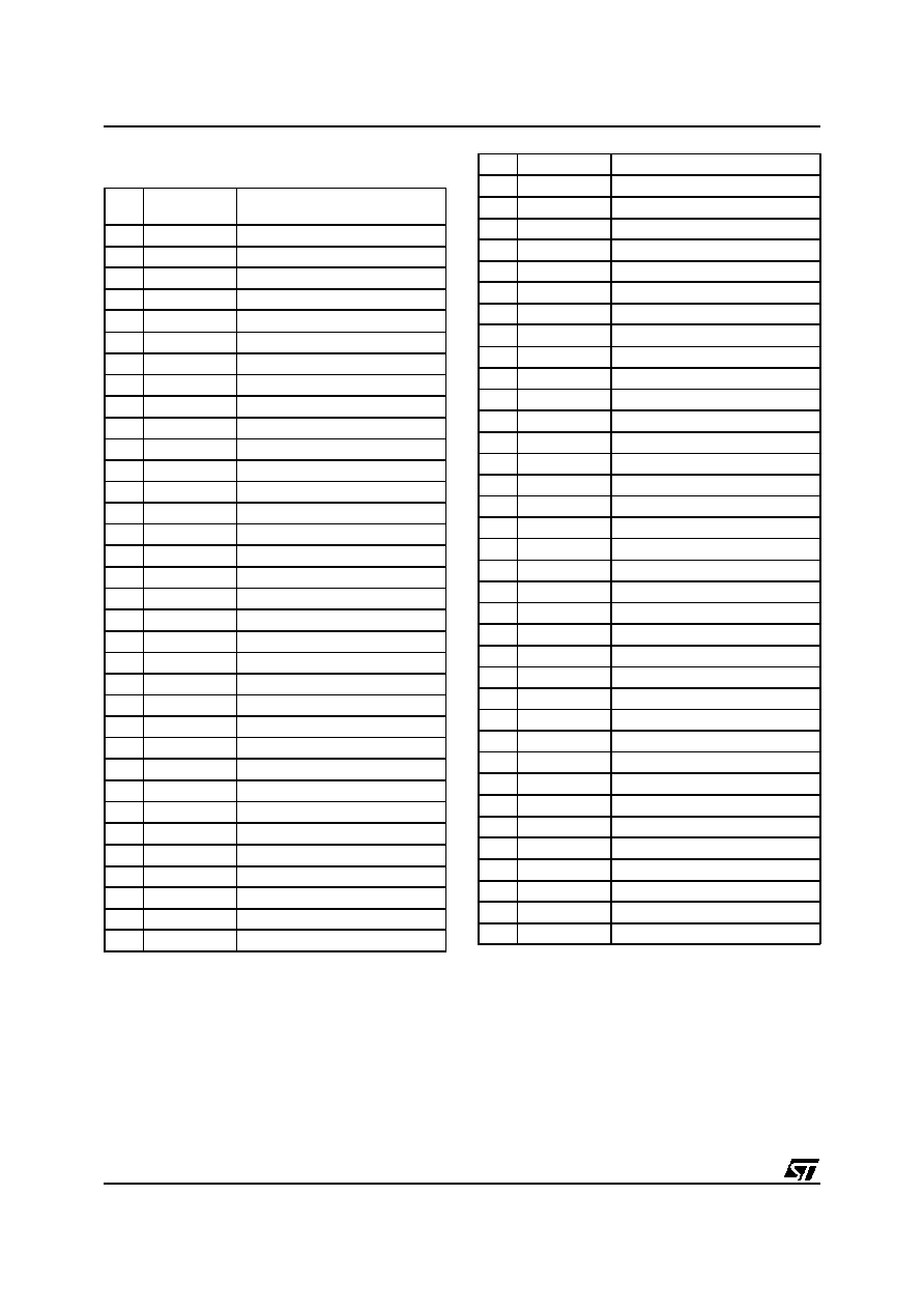
Table 3. Top Boot Block Addresses,
M28W320CT
#
Size
(KWord)
Address Range
70
4
1FF000-1FFFFF
69
4
1FE000-1FEFFF
68
4
1FD000-1FDFFF
67
4
1FC000-1FCFFF
66
4
1FB000-1FBFFF
65
4
1FA000-1FAFFF
64
4
1F9000-1F9FFF
63
4
1F8000-1F8FFF
62
32
1F0000-1F7FFF
61
32
1E8000-1EFFFF
60
32
1E0000-1E7FFF
59
32
1D8000-1DFFFF
58
32
1D0000-1D7FFF
57
32
1C8000-1CFFFF
56
32
1C0000-1C7FFF
55
32
1B8000-1BFFFF
54
32
1B0000-1B7FFF
53
32
1A8000-1AFFFF
52
32
1A0000-1A7FFF
51
32
198000-19FFFF
50
32
190000-197FFF
49
32
188000-18FFFF
48
32
180000-187FFF
47
32
178000-17FFFF
46
32
170000-177FFF
45
32
168000-16FFFF
44
32
160000-167FFF
43
32
158000-15FFFF
42
32
150000-157FFF
41
32
148000-14FFFF
40
32
140000-147FFF
39
32
138000-13FFFF
38
32
130000-137FFF
37
32
128000-12FFFF
36
32
120000-127FFF
35
32
118000-11FFFF
34
32
110000-117FFF
33
32
108000-10FFFF
32
32
100000-107FFF
31
32
0F8000-0FFFFF
30
32
0F00000-F7FFF
29
32
0E8000-0EFFFF
28
32
0E0000-0E7FFF
27
32
0D8000-0DFFFF
26
32
0D0000-0D7FFF
25
32
0C8000-0CFFFF
24
32
0C0000-0C7FFF
23
32
0B8000-0BFFFF
22
32
0B0000-0B7FFF
21
32
0A8000-0AFFFF
20
32
0A0000-0A7FFF
19
32
098000-09FFFF
18
32
090000-097FFF
17
32
088000-08FFFF
16
32
080000-087FFF
15
32
078000-07FFFF
14
32
070000-077FFF
13
32
068000-06FFFF
12
32
060000-067FFF
11
32
058000-05FFFF
10
32
050000-057FFF
9
32
048000-04FFFF
8
32
040000-047FFF
7
32
038000-03FFFF
6
32
030000-037FFF
5
32
028000-02FFFF
4
32
020000-027FFF
3
32
018000-01FFFF
2
32
010000-017FFF
1
32
008000-00FFFF
0
32
000000-007FFF
5/42
M28W320CT, M28W320CB
36
32
0E8000-0EFFFF
35
32
0E0000-0E7FFF
34
32
0D8000-0DFFFF
33
32
0D0000-0D7FFF
32
32
0C8000-0CFFFF
31
32
0C0000-0C7FFF
30
32
0B8000-0BFFFF
29
32
0B0000-0B7FFF
28
32
0A8000-0AFFFF
27
32
0A0000-0A7FFF
26
32
098000-09FFFF
25
32
090000-097FFF
24
32
088000-08FFFF
23
32
080000-087FFF
22
32
078000-07FFFF
21
32
070000-077FFF
20
32
068000-06FFFF
19
32
060000-067FFF
18
32
058000-05FFFF
17
32
050000-057FFF
16
32
048000-04FFFF
15
32
040000-047FFF
14
32
038000-03FFFF
13
32
030000-037FFF
12
32
028000-02FFFF
11
32
020000-027FFF
10
32
018000-01FFFF
9
32
010000-017FFF
8
32
008000-00FFFF
7
4
007000-007FFF
6
4
006000-006FFF
5
4
005000-005FFF
4
4
004000-004FFF
3
4
003000-003FFF
2
4
002000-002FFF
1
4
001000-001FFF
0
4
000000-000FFF
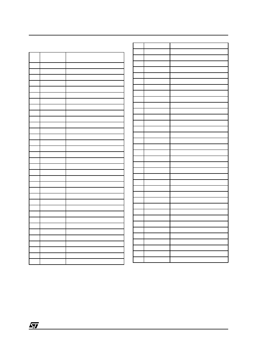
Table 4. Bottom Boot Block Addresses,
M28W320CB
#
Size
(KWord)
Address Range
70
32
1F8000-1FFFFF
69
32
1F0000-1F7FFF
68
32
1E8000-1EFFFF
67
32
1E0000-1E7FFF
66
32
1D8000-1DFFFF
65
32
1D0000-1D7FFF
64
32
1C8000-1CFFFF
63
32
1C0000-1C7FFF
62
32
1B8000-1BFFFF
61
32
1B0000-1B7FFF
60
32
1A8000-1AFFFF
59
32
1A0000-1A7FFF
58
32
198000-19FFFF
57
32
190000-197FFF
56
32
188000-18FFFF
55
32
180000-187FFF
54
32
178000-17FFFF
53
32
170000-177FFF
52
32
168000-16FFFF
51
32
160000-167FFF
50
32
158000-15FFFF
49
32
150000-157FFF
48
32
148000-14FFFF
47
32
140000-147FFF
46
32
138000-13FFFF
45
32
130000-137FFF
44
32
128000-12FFFF
43
32
120000-127FFF
42
32
118000-11FFFF
41
32
110000-117FFF
40
32
108000-10FFFF
39
32
100000-107FFF
38
32
0F8000-0FFFFF
37
32
0F0000-0F7FFF