
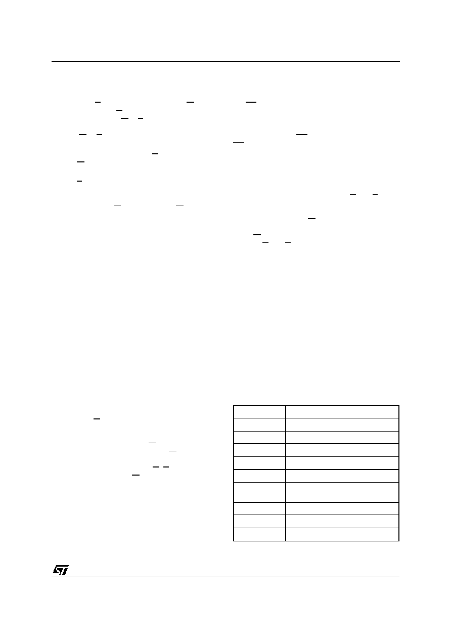
AI02078C
18
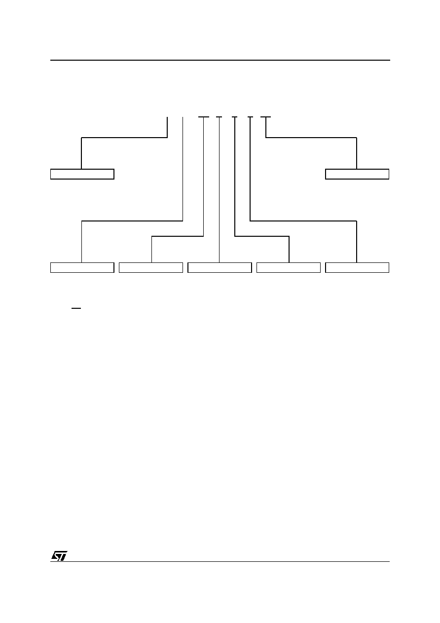
A0-A17
W
DQ0-DQ7
VCC
M29F002T
M29F002B
M29F002NT
E
VSS
8
G
(*) RPNC
Figure 1. Logic Diagram
M29F002T, M29F002NT
M29F002B
2 Mbit (256Kb x8, Boot Block) Single Supply Flash Memory
5V
±
10% SUPPLY VOLTAGE for PROGRAM,
ERASE and READ OPERATIONS
FAST ACCESS TIME: 70ns
FAST PROGRAMMING TIME: 10
µ
s typical
PROGRAM/ERASE CONTROLLER (P/E.C.)
≠ Program Byte-by-Byte
≠ Status Register bits
MEMORY BLOCKS
≠ Boot Block (Top or Bottom location)
≠ Parameter and Main blocks
BLOCK, MULTI-BLOCK and CHIP ERASE
MULTI-BLOCK PROTECTION/TEMPORARY
UNPROTECTION MODES
ERASE SUSPEND and RESUME MODES
≠ Read and Program another Block during
Erase Suspend
LOW POWER CONSUMPTION
≠ Stand-by and Automatic Stand-by
100,000 PROGRAM/ERASE CYCLES per
BLOCK
20 YEARS DATA RETENTION
≠ Defectivity below 1ppm/year
ELECTRONIC SIGNATURE
≠ Manufacturer Code: 20h
≠ Device Code, M29F002T: B0h
≠ Device Code, M29F002NT: B0h
≠ Device Code, M29F002B: 34h
DESCRIPTION
The M29F002 is a non-volatile memory that may
be erased electrically at the block or chip level and
programmed in-system on a Byte-by-Byte basis
using only a single 5V V
CC
supply.For Program and
Erase operations the necessary high voltages are
generated internally. The device can also be pro-
grammed in standard programmers.
The array matrix organisation allows each block to
be erased and reprogrammed without affecting
other blocks. Blocks can be protected against pro-
graming and erase on programming equipment,
and temporarily unprotected to make changes in
the application. Each block can be programmed
and erased over 100,000 cycles.
July 1998
1/29
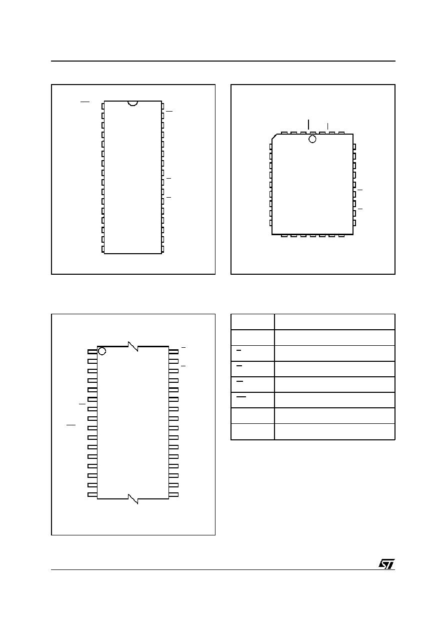
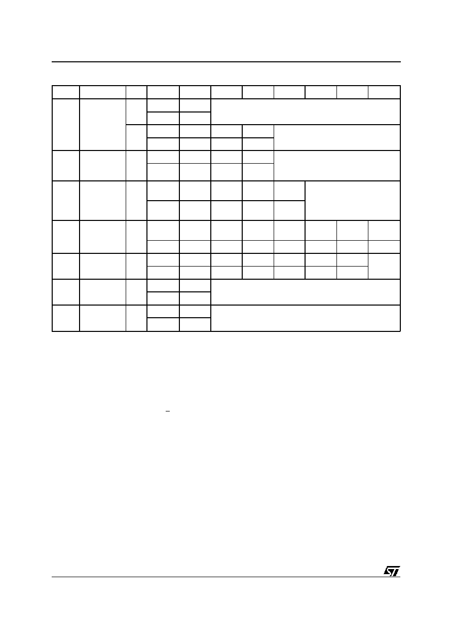
PLCC32 (K)
32
1
PDIP32 (P)
TSOP32 (N)
8 x 20mm
Note: * RPNC function is not available for the M29F002NT
AI02079C
A17
A13
A10
DQ5
17
A1
A0
DQ0
DQ1
DQ2
DQ3
DQ4
A7
A4
A3
A2
A6
A5
9
W
A8
1
A16
A9
DQ7
A12
A14
32
RPNC
V
CC
M29F002T
M29F002B
A15
A11
DQ6
G
E
25
V
SS
Figure 2B. LCC Pin Connections
A1
A0
DQ0
A7
A4
A3
A2
A6
A5
A13
A10
A8
A9
DQ7
A14
A11
G
E
DQ5
DQ1
DQ2
DQ3
VSS
DQ4
DQ6
A17
W
A16
A12
(*) RPNC
VCC
A15
AI02080C
M29F002T
M29F002B
M29F002NT
8
1
2
3
4
5
6
7
9
10
11
12
13
14
15
16
32
31
30
29
28
27
26
25
24
23
22
21
20
19
18
17
Figure 2A. DIP Pin Connections
A1
A0
DQ0
A7
A4
A3
A2
A6
A5
A13
A10
A8
A9
DQ7
A14
A11
G
E
DQ5
DQ1
DQ2
DQ3
DQ4
DQ6
A17
W
A16
A12
RPNC
VCC
A15
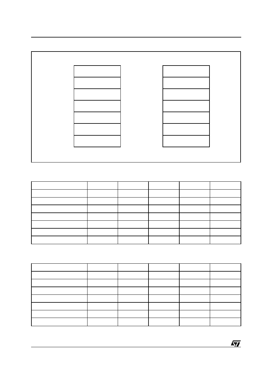
AI02361B
M29F002T
M29F002B
8
1
9
16
17
24
25
32
VSS
Figure 2C. TSOP Pin Connections
Note: Pin 1 is not connected for the M29F002NT
A0-A17
Address Inputs
DQ0-DQ7
Data Input/Outputs, Command Inputs
E
Chip Enable
G
Output Enable
W
Write Enable
RPNC
(*)
Reset / Block Temporary Unprotect
V
CC
Supply Voltage
V
SS
Ground
Table 1. Signal Names
DESCRIPTION (cont'd)
Instructions for Read/Reset, Auto Select for read-
ing the Electronic Signature or Block Protection
status, Programming, Block and Chip Erase, Erase
Suspend and Resume are written to the device in
cycles of commands to a Command Interfaceusing
standard microprocessor write timings. The device
is offered in PLCC32, PDIP32 and TSOP32 (8 x 20
mm) packages.
2/29
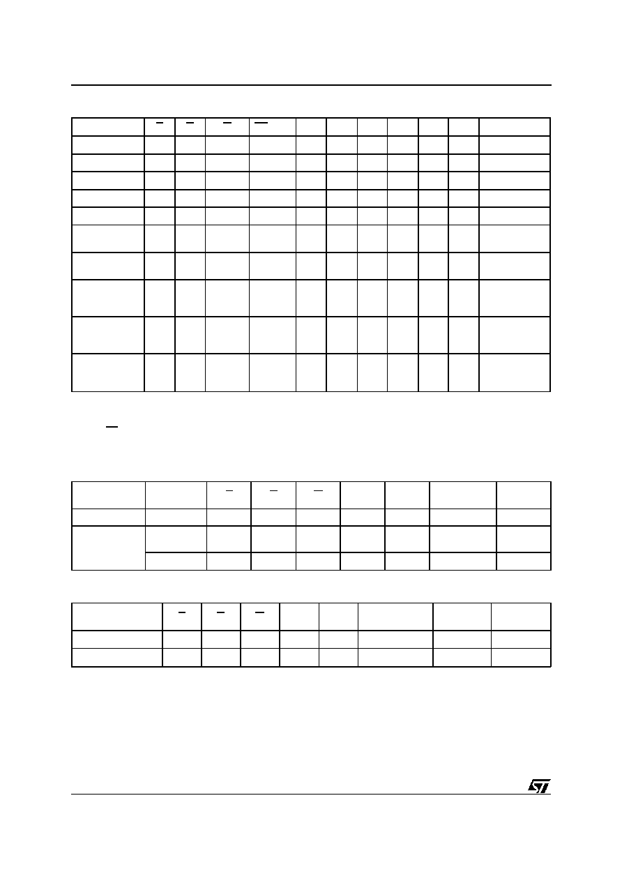
M29F002T, M29F002NT, M29F002B
Symbol
Parameter
Value
Unit
T
A
Ambient Operating Temperature
(3)
≠40 to 125
∞
C
T
BIAS
Temperature Under Bias
≠50 to 125
∞
C
T
STG
Storage Temperature
≠65 to 150
∞
C
V
IO
(2)
Input or Output Voltages
≠0.6 to 7
V
V
CC
Supply Voltage
≠0.6 to 7
V
V
(A9, E, G, RPNC)
(2)
A9, E, G, RPNC Voltage
≠0.6 to 13.5
V
Notes: 1. Except for the rating "Operating Temperature Range", stresses above those listed in the Table "Absolute Maximum Ratings"
may cause permanent damage to the device. These are stress ratings only and operation of the device at these or any other
conditions above those indicated in the Operating sections of this specification is not i mplied. Exposure to Absolute Maximum
Rating conditions for extended periods may affect device reliability. Refer also to the STMicroelectronics SURE Program and other
relevant quality documents.
2. Minimum Voltage may undershoot to ≠2V during transition and for less than 20ns.
3. Depends on range.
Table 2. Absolute Maximum Ratings
(1)
Organisation
The M29F002 is organised as 256K x 8. Memory
control is provided by Chip Enable E, Output En-
able G and Write Enable W inputs.
A Reset/Block Temporary Unprotection RPNC
(NOT available on M29F002NT) tri-level input pro-
vides a hardwarereset when pulled Low, and when
held High (at V
ID
) temporarily unprotects blocks
previously protected allowing them to be progra-
med and erased. Erase and Program operations
are controlled by an internal Program/Erase Con-
troller (P/E.C.).StatusRegister data outputon DQ7
provides a Data Polling signal, and DQ6 and DQ2
provide Toggle signals to indicate the state of the
P/E.C operations.
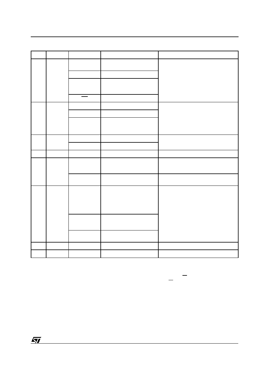
Memory Blocks
The devices feature asymmetrically blocked archi-
tecture providing system memory integration. The
M29F002 has an array of 7 blocks, one Boot Block
of 16 KBytes, two Parameter Blocks of 8 KBytes,
one Main Block of 32 KBytes and three Main Blocks
of 64 KBytes.
The memory map is shown in Figure 3. Each block
can be erased separately, any combination of
blocks can be specified for multi-block erase or the
entire chip may be erased. The Erase operations
are managedautomaticallyby the P/E.C.The block
erase operation can be suspended in order to read
from or program to any block not being ersased,
and then resumed. Block protection provides addi-
tional data security. Each block can be separately
protectedor unprotectedagainstProgram or Erase
on programming equipment. All previously pro-
tected blocks can be temporarily unprotectedin the
application.
Bus Operations
The following operations can be performed using
the appropriate bus cycles: Read (Array, Electronic
Signature, Block Protection Status), Write com-
mand, Output Disable, Standby, Reset, Block Pro-
t ec t i o n , U np r o t e ct i o n, P ro t e cti on Ver i f y,
Unprotection Verify and Block Temporary Unpro-
tection. See Tables 4 and 5.
Command Interface
Instructions, made up of commands written in cy-
cles, can be given to the Program/EraseController
through a Command Interface (C.I.). For added
data protection, program or erase execution starts
after 4 or 6 cycles. The first, second, fourth and fifth
cycles are used to input Coded cycles to the C.I.
This Coded sequence is the same for all Pro-
gram/Erase Controller instructions. The 'Com-
mand' itself and its confirmation, when applicable,
are given on the third, fourth or sixth cycles. Any
incorrect command or any improper command se-
quence will reset the device to Read Array mode.
3/29
M29F002T, M29F002NT, M29F002B
Address Range
A17
A16
A15
A14
A13
00000h-0FFFFh
0
0
X
X
X
10000h-1FFFFh
0
1
X
X
X
20000h-2FFFFh
1
0
X
X
X
30000h-37FFFh
1
1
0
X
X
38000h-39FFFh
1
1
1
0
0
3A000h-3BFFFh
1
1
1
0
1
3C000h-3FFFFh
1
1
1
1
X
Table 3A. M29F002T, M29F002NT Block Address Table
Address Range
A17
A16
A15
A14
A13
00000h-03FFFh
0
0
0
0
X
04000h-05FFFh
0
0
0
1
0
06000h-07FFFh
0
0
0
1
1
08000h-0FFFFh
0
0
1
X
X
10000h-1FFFFh
0
1
X
X
X
20000h-2FFFFh
1
0
X
X
X
30000h-3FFFFh
1
1
X
X
X
Table 3B. M29F002B Block Address Table
AI02081C
16K BOOT BLOCK
3FFFFh
3C000h
3BFFFh
3A000h
39FFFh
00000h
8K PARAMETER BLOCK
8K PARAMETER BLOCK
32K MAIN BLOCK
64K MAIN BLOCK
64K MAIN BLOCK
64K MAIN BLOCK
M29F002T, M29F002NT
38000h
37FFFh
30000h
2FFFFh
20000h
1FFFFh
10000h
0FFFFh
3FFFFh
30000h
2FFFFh
20000h
1FFFFh
00000h
8K PARAMETER BLOCK
8K PARAMETER BLOCK
32K MAIN BLOCK
64K MAIN BLOCK
64K MAIN BLOCK
64K MAIN BLOCK
M29F002B
10000h
0FFFFh
08000h
07FFFh
06000h
05FFFh
04000h
03FFFh
16K BOOT BLOCK
Figure 3. Memory Map and Block Address Table
4/29
M29F002T, M29F002NT, M29F002B

Instructions
Seven instructions are defined to perform Read
Array, Auto Select (to read the ElectronicSignature
or Block Protection Status), Program, Block Erase,
Chip Erase, Erase Suspend and Erase Resume.
The internal P/E.C. automatically handles all tim-
ing and verification of the Program and Erase
operations. The Status Register Data Polling, Tog-
gle, Error bits may be read at any time, during
programming or erase, to monitor the progress of
the operation.
Instructions are composed of up to six cycles. The
first two cycles input a Coded sequence to the
Command Interfacewhich is common to all instruc-
tions (see Table 8). The third cycle inputs the
instruction set-up command. Subsequent cycles
output the addressed data, Electronic Signature or
Block Protection Status for Read operations. In
order to give additional data protection, the instruc-
tions for Program and Block or Chip Erase require
further command inputs. For a Program instruction,
the fourth command cycle inputs the address and
data to be programmed. For an Erase instruction
(Block or Chip), the fourth and fifth cycles input a
further Coded sequence before the Erase confirm
command on the sixth cycle. Erasure of a memory
block may be suspended,in orderto read data from
another block or to program data in another block,
and then resumed.
When power is first applied or if V
CC
falls below
V
LKO
, the command interface is reset to Read
Array.
SIGNAL DESCRIPTIONS
See Figure 1 and Table 1.
Address Inputs (A0-A17). The address inputs for
the memory array are latched during a write opera-
tion on the falling edge of Chip Enable E or Write
Enable W. When A9 is raised to V
ID
, either a Read
ElectronicSignature Manufactureror Device Code,
Block Protection Status or a Write Block Protection
or Block Unprotection is enabled depending on the
combination of levels on A0, A1, A6, A12 and A15.
Data Input/Outputs (DQ0-DQ7). The input is data
to be programmed in the memory array or a com-
mand to be written to the C.I. Both are latched on
the rising edge of Chip Enable E or Write Enable
W. The output is data from the Memory Array, the
Electronic Signature Manufacturer or Device
codes, the Block Protection Status or the Status
register Data Polling bit DQ7, the Toggle Bits DQ6
and DQ2, the Error bit DQ5 or the Erase Timer bit
DQ3. Outputs are valid when Chip Enable E and
Output Enable G are active. The output is high
impedance when the chip is deselected or the
outputs are disabled and when RPNC is at a Low
level.
Chip Enable (E). The Chip Enable input activates
the memory control logic, input buffers, decoders
and sense amplifiers. E High deselectsthe memory
and reduces the power consumption to the standby
level. E can also be used to control writing to the
command register and to the memory array, while
W remains at a low level. The Chip Enable must be
forced to V
ID
during the Block Unprotection opera-
tion.
Output Enable (G). The Output Enable gates the
outputs through the data buffers during a read
operation. When G is High the outputs are High
impedance. G must be forced to V
ID
level during
Block Protection and Unprotection operations.
Write Enable (W). This input controls writing to the
Command Registerand Addressand Data latches.
Reset/Block Temporary Unprotect/No Connect
Input (RPNC). The RPNC (not available for the
M29F002NT) input provides hardware reset and
protected block(s) temporary unprotection func-
tions. In read or write mode, the RPNC pin can be
left open (Not Connected) or held at V
IH
. Reset of
the memory is acheived by pulling RPNC to V
IL
for
at least 500ns. When the reset pulse is given, if the
memory is in Read or Standby modes, it will be
available for new operations in 50ns after the rising
edge of RPNC. If the memory is in Erase, Erase
Suspend or Program modes the reset will take
10
µ
s. Ahardware reset duringan Eraseor Program
operation will corrupt the data being programmed
or the sector(s) being erased.
Temporary block unprotection is made by holding
RPNC at V
ID
. In this condition previously protected
blocks can be programmed or erased. The transi-
tion of RPNC from V
IH
to V
ID
must slower than
500ns. When RPNC is returned from V
ID
to V
IH
all
blocks temporarily unprotected will be again pro-
tected.
V
CC
Supply Voltage. The power supply for all
operations (Read, Program and Erase).
V
SS
Ground. V
SS
is the reference for all voltage
measurements.
DEVICE OPERATIONS
See Tables 4, 5 and 6.
Read. Read operations are used to output the
contents of the Memory Array, the Electronic Sig-
nature, the Status Register or the Block Protection
Status. Both Chip Enable E and Output Enable G
must be low in order to read the output of the
memory.
5/29
M29F002T, M29F002NT, M29F002B
Operation
E
G
W
RPNC
(6)
A0
A1
A6
A9
A12
A15
DQ0-DQ7
Read Byte
V
IL
V
IL
V
IH
V
IH
/NC
(5)
A0
A1
A6
A9
A12
A15
Data Output
Write Byte
V
IL
V
IH
V
IL
V
IH
/NC
(5)
A0
A1
A6
A9
A12
A15
Data Input
Output Disable
V
IL
V
IH
V
IH
V
IH
/NC
(5)
X
X
X
X
X
X
Hi-Z
Standby
V
IH
X
X
V
IH
/NC
(5)
X
X
X
X
X
X
Hi-Z
Reset
(6)
X
X
X
V
IL
X
X
X
X
X
X
Hi-Z
Block
Protection
(2,4)
V
IL
V
ID
V
IL
Pulse
V
IH
/NC
(5)
X
X
X
V
ID
X
X
X
Blocks
Unprotection
(4)
V
ID
V
ID
V
IL
Pulse
V
IH
/NC
(5)
X
X
X
V
ID
V
IH
V
IH
X
Block
Protection
Verify
(2,4)
V
IL
V
IL
V
IH
V
IH
/NC
(5)
V
IL
V
IH
V
IL
V
ID
A12
A15
Block Protect
Status
(3)
Block
Unprotection
Verify
(2,4)
V
IL
V
IL
V
IH
V
IH
/NC
(5)
V
IL
V
IH
V
IH
V
ID
A12
A15
Block Protect
Status
(3)
Block
Temporary
Unprotection
(6)
X
X
X
V
ID
X
X
X
X
X
X
X
Notes: 1. X = V
IL
or V
IH
2. Block Address must be given on A13-A17 bits.
3. See Table 6.
4. Operation performed on programming equipment.
5. RPNC can be held at V
IH
or left open (Not Connected).
6. Not Available on M29F002NT.
Table 4. User Bus Operations
(1)
Code
Device
E
G
W
A0
A1
Other
Addresses
DQ0 - DQ7
Manufact. Code
V
IL
V
IL
V
IH
V
IL
V
IL
Don't Care
20h
Device Code
M29F002T
M29F002NT
V
IL
V
IL
V
IH
V
IH
V
IL
Don't Care
B0h
M29F002B
V
IL
VIL
V
IH
V
IH
V
IL
Don't Care
34h
Table 5. Read Electronic Signature (following AS instruction or with A9 = V
ID
)
Code
E
G
W
A0
A1
A13 - A17
Other
Addresses
DQ0 - DQ7
Protected Block
V
IL
V
IL
V
IH
V
IL
V
IH
Block Address
Don't Care
01h
Unprotected Block
V
IL
V
IL
V
IH
V
IL
V
IH
Block Address
Don't Care
00h
Table 6. Read Block Protection with AS Instruction
6/29
M29F002T, M29F002NT, M29F002B
Write. Write operations are used to give Instruction
Commands to the memory or to latch input data to
be programmed. A write operation is initiated when
Chip Enable E is Low and Write Enable W is Low
with Output Enable G High. Addresses are latched
on the falling edge of W or E whichever occurs last.
Commands and Input Data are latchedon the rising
edge of W or E whichever occurs first.
Output Disable. The data outputs are high imped-
ance when the Output Enable G is High with Write
Enable W High.
Standby. The memory is in standby when Chip
Enable E is High and the P/E.C. is idle. The power
consumption is reduced to the standby level and
the outputs are high impedance, independent of
the Output Enable G or Write Enable W inputs.
Automatic Standby. After 150ns of bus inactivity
and when CMOS levels are driving the addresses,
the chip automatically enters a pseudo-standby
mode where consumption is reduced to the CMOS
standby value, while outputs still drive the bus.
Electronic Signature. Two codes identifying the
manufacturerand the device can be read from the
memory. These codes allow programming equip-
ment or applications to automatically match their
interface to the characteristics of the M29F002.
The Electronic Signature is output by a Read op-
eration when the voltage applied to A9 is at V
ID
and
address input A1 is Low. The manufacturer code is
output when the Address input A0 is Low and the
device code when this input is High. Other Address
inputs are ignored.
The Electronic Signature can also be read, without
raising A9 to V
ID
, by giving the memory the Instruc-
tion AS.
Block Protection. Each block can be separately
protected against Program or Erase on program-
ming equipment. Block protection provides addi-
tional data security, as it disables all program or
erase operations. This mode is activated when
both A9 and G are raised to V
ID
and an address in
the block is applied on A13-A17. The Block Protec-
tion algorithm is shown in Figure 14. Block protec-
tion is initiated on the edge of W falling to V
IL
. Then
after a delay of 100
µ
s, the edge of W rising to V
IH
ends the protection operations. Block protection
verify is achieved by bringing G, E, A0 and A6 to
V
IL
and A1 to V
IH
, while W is at V
IH
and A9 at V
ID
.
Under these conditions, reading the dataoutput will
yield 01h if the block defined by the inputs on
A13-A17 is protected. Any attempt to program or
erase a protected block will be ignored by the
device.
Block Temporary Unprotection. This feature is
available on M29F002T and M29F002B only. Any
previously protected block can be temporarily un-
protected in order to change stored data. The
temporaryunprotectionmode is activated by bring-
ing RPNC to V
ID
. During the temporary unprotec-
tion mode the previously protected blocks are
unprotected.A block can be selected and data can
be modified by executing the Erase or Program
instruction with the RPNC signal held at V
ID
. When
RPNC is returned to V
IH
, all the previously pro-
tected blocks are again protected.
Block Unprotection. All protected blocks can be
unprotected on programming equipment to allow
updating of bit contents. All blocks must first be
protected before the unprotection operation. Block
unprotection is activated when A9, G and E are at
V
ID
and A12, A15 at V
IH
. The Block Unprotection
algorithm is shown in Figure 15. Unprotection is
initiated by the edge of W falling to V
IL
. After a delay
of 10ms, the unprotection operation is ended by
rising W to V
IH
. Unprotection verify is achieved by
bringing G and E to V
IL
while A0 is at V
IL
, A6 and
A1 are at V
IH
and A9 remains at V
ID
. In these
conditions, reading the output data will yield 00h if
the block defined by the inputs A13-A17 has been
succesfullyunprotected.Each block must be sepa-
rately verified by giving its address in order to
ensure that it has been unprotected.
INSTRUCTIONS AND COMMANDS
The Command Interface latches commands writ-
ten to the memory. Instructions are made up from
one or more commands to perform Read Memory
Array, Read Electronic Signature, Read Block Pro-
tection, Program, Block Erase, Chip Erase, Erase
Suspend and Erase Resume. Commands are
made of address and data sequences.
Hex Code
Command
00h
Invalid/Reserved
10h
Chip Erase Confirm
20h
Reserved
30h
Block Erase Resume/Confirm
80h
Set-up Erase
90h
Read Electronic Signature/
Block Protection Status
A0h
Program
B0h
Erase Suspend
F0h
Read Array/Reset
Table 7. Commands
7/29
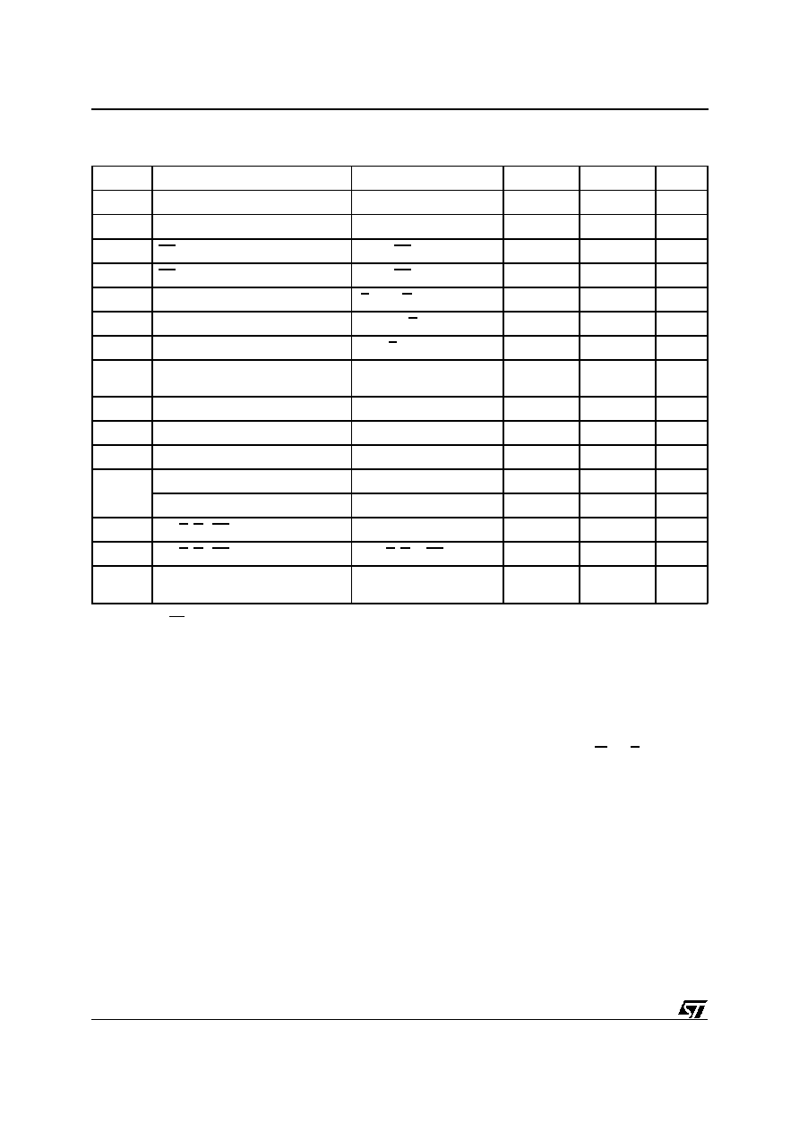
M29F002T, M29F002NT, M29F002B
Mne.
Instr.
Cyc.
1st Cyc. 2nd Cyc. 3rd Cyc. 4th Cyc. 5th Cyc. 6th Cyc. 7th Cyc.
RD
(2,4)
Read/Reset
Memory Array
1+
Addr.
(3,7)
X
Read Memory Array until a new write cycle is initiated.
Data
F0h
3+
Addr.
(3,7)
555h
AAAh
555h
Read Memory Array until a new write
cycle is initiated.
Data
AAh
55h
F0h
AS
(4)
Auto Select
3+
Addr.
(3,7)
555h
AAAh
555h
Read Electronic Signature or Block
Protection Status until a new write cycle
is initiated. See Note 5 and 6.
Data
AAh
55h
90h
PG
Program
4
Addr.
(3,7)
555h
AAAh
555h
Program
Address Read Data Polling or Toggle
Bit until Program completes.
Data
AAh
55h
A0h
Program
Data
BE
Block Erase
6
Addr.
(3,7)
555h
AAAh
555h
555h
AAAh
Block
Address
Additional
Block
(8)
Data
AAh
55h
80h
AAh
55h
30h
30h
CE
Chip Erase
6
Addr.
(3,7)
555h
AAAh
555h
555h
AAAh
555h
Note 9
Data
AAh
55h
80h
AAh
55h
10h
ES
(10)
Erase
Suspend
1
Addr.
(3,7)
X
Read until Toggle stops, then read all the data needed from
any Block(s) not being erased then Resume Erase.
Data
B0h
ER
Erase
Resume
1
Addr.
(3,7)
X
Read Data Polling or Toggle Bits until Erase completes or
Erase is suspended another time
Data
30h
Notes: 1. Commands not interpreted in this table will default to read array mode.
2. A wait of t
PLYH
is necessary after a Read/Reset command if the memory was in an Erase or Program mode
before starting any new operation (see Table 14 and Figure 9).
3. X = Don't Care.
4. The first cycles of the RD or AS instructions are followed by read operations. Any number of read cycles can occur after
the command cycles.
5. Signature Address bits A0, A1 at V
IL
will output Manufacturer code (20h). Address bits A0 at V
IH
and A1 at V
IL
will output
Device code.
6. Block Protection Address: A0 at V
IL
, A1 at V
IH
and A13-A17 within the Block will output the Block Protection status.
7. For Coded cycles address inputs A12-A17 are don't care.
8. Optional, additional Blocks addresses must be entered within the erase timeout delay after last write entry,
timeout status can be verified through DQ3 value (see Erase Timer Bit DQ3 description).
When full command is entered, read Data Polling or Toggle bit until Erase is completed or suspended.
9. Read Data Polling, Toggle bits or RB until Erase completes.
10.During Erase Suspend, Read and Data Program functions are allowed in blocks not being erased.
Table 8. Instructions
(1)
The instructions require from 1 to 6 cycles, the first
or first three of which are always write operations
used to initiate the instruction.They are followed by
either further write cycles to confirm the first com-
mand or execute the command immediately. Com-
mand sequencing must be followed exactly. Any
invalid combination of commands will reset the
device to Read Array. The increased number of
cycles has been chosen to assure maximum data
security. Instructions are initialised by two initial
Coded cycles which unlock the Command Inter-
face. In addition, for Erase, instruction confirmation
is again preceded by the two Coded cycles.
Status Register Bits
P/E.C. status is indicated during execution by Data
Polling on DQ7, detection of Toggle on DQ6 and
DQ2, or Error on DQ5 and Erase Timer DQ3 bits.
Any read attempt during Program or Erase com-
mand execution will automatically output these five
Status Register bits. The P/E.C. automatically sets
bits DQ2, DQ3, DQ5, DQ6 and DQ7. Other bits
(DQ0, DQ1 and DQ4) are reserved for future use
and should be masked. See Tables 9 and 10.
8/29
M29F002T, M29F002NT, M29F002B
DQ
Name
Logic Level
Definition
Note
7
Data
Polling
'1'
Erase Complete or erase
block in Erase Suspend
Indicates the P/E.C. status, check during
Program or Erase, and on completion
before checking bits DQ5 for Program or
Erase Success.
'0'
Erase On-going
DQ
Program Complete or data
of non erase block during
Erase Suspend
DQ
Program On-going
6
Toggle Bit
'-1-0-1-0-1-0-1-'
Erase or Program On-going
Successive reads output complementary
data on DQ6 while Programming or Erase
operations are on-going. DQ6 remains at
constant level when P/E.C. operations are
completed or Erase Suspend is
acknowledged.
DQ
Program Complete
'-1-1-1-1-1-1-1-'
Erase Complete or Erase
Suspend on currently
addressed block
5
Error Bit
'1'
Program or Erase Error
This bit is set to '1' in the case of
Programming or Erase failure.
'0'
Program or Erase On-going
4
Reserved
3
Erase
Time Bit
'1'
Erase Timeout Period Expired
P/E.C. Erase operation has started. Only
possible command entry is Erase Suspend
(ES).
'0'
Erase Timeout Period
On-going
An additional block to be erased in parallel
can be entered to the P/E.C.
2
Toggle Bit
'-1-0-1-0-1-0-1-'
Chip Erase, Erase or Erase
Suspend on the currently
addressed block.
Erase Error due to the
currently addressed block
(when DQ5 = '1').
Indicates the erase status and allows to
identify the erased block
1
Program on-going, Erase
on-going on another block or
Erase Complete
DQ
Erase Suspend read on
non Erase Suspend block
1
Reserved
0
Reserved
Notes: Logic level '1' is High, '0' is Low. -0-1-0-0-0-1-1-1-0- represent bit value in successive Read operations.
Table 9. Status Register Bits
Data Polling Bit (DQ7). When Programming op-
erations are in progress, this bit outputs the com-
plement of the bit being programmed on DQ7.
During Erase operation, it outputs a '0'. After com-
pletion of the operation, DQ7 will output the bit last
programmed or a '1' after erasing. Data Polling is
valid and only effective during P/E.C. operation,
that is after the fourth W pulse for programming or
after the sixth W pulse for erase. It must be per-
formed at the address being programmed or at an
address within the block being erased. If all the
blocks selected for erasure are protected, DQ7 will
be set to '0' for about 100
µ
s, and then return to the
previous addressed memory data value.
9/29
M29F002T, M29F002NT, M29F002B
See Figure 11 for the Data Polling flowchart and
Figure 10 for the Data Polling waveforms. DQ7 will
also flag the Erase Suspend mode by switching
from '0' to '1' at the start of the Erase Suspend. In
order to monitor DQ7 in the Erase Suspend mode
an address within a block being erased must be
provided. For a Read Operationin Erase Suspend
mode, DQ7 will output '1' if the read is attempted
on a blockbeing erased and the datavalue on other
blocks. During Program operation in Erase Sus-
pend Mode, DQ7 will have the same behaviour as
in the normal program execution outside of the
suspend mode.
Toggle Bit (DQ6). When Programming or Erasing
operations are in progress, successive attempts to
read DQ6 will output complementarydata. DQ6 will
toggle following toggling of either G, or E when G
is low. The operation is completed when two suc-
cessive reads yield the same output data. The next
read will output the bit last programmed or a '1' after
erasing. The toggle bit DQ6 is valid only during
P/E.C. operations, that is after the fourth W pulse
for programming or after the sixth W pulse for
Erase. If the blocks selected for erasure are pro-
tected, DQ6 will toggle for about 100
µ
s and then
return back to Read. DQ6 will be set to '1' if a Read
operationis attemptedon an Erase Suspendblock.
When erase is suspended DQ6 will toggle during
programming operations in a block different to the
block in Erase Suspend. Either E or G toggling will
cause DQ6 to toggle. See Figure 12 for Toggle Bit
flowchart and Figure 13 for Toggle Bit waveforms.
Toggle Bit (DQ2). This toggle bit, together with
DQ6, can be used to determine the device status
during the Erase operations. It can also be used to
identify the block being erased. During Erase or
Erase Suspend a read from a block being erased
will cause DQ2 to toggle. A read from a block not
being erased will set DQ2 to '1' during erase and
to DQ2 during Erase Suspend. During Chip Erase
a read operation will cause DQ2 to toggle as all
blocks are being erased. DQ2 will be set to '1'
during program operation and when erase is com-
plete. After erase completion and if the error bit
DQ5 is set to '1', DQ2 will toggle if the faulty block
is addressed.
Error Bit (DQ5). This bit is set to '1' by the P/E.C.
when there is a failure of programming, block
erase, or chip erase that results in invalid data in
the memory block. In case of an error in block erase
or program, the block in which the error occured or
to which the programmed data belongs, must be
discarded. The DQ5 failure condition will also ap-
pear if a user tries to program a '1' to a location that
is previously programmed to '0'. Other Blocks may
stillbe used.The error bit resets after a Read/Reset
(RD) instruction. In case of success of Program or
Erase, the error bit will be set to '0' .
Erase Timer Bit (DQ3). This bit is set to '0' by the
P/E.C. when the last block Erase command has
been entered to the Command Interface and it is
awaiting the Erase start. When the erase timeout
period is finished, after 50
µ
s to 120
µ
s, DQ3 returns
to '1'.
Coded Cycles
The two Coded cycles unlock the Command Inter-
face. They are followed by an input command or a
confirmation command. The Coded cycles consist
of writing the data AAh at address 555h during the
first cycle. During the second cycle the Coded
cycles consist of writing the data 55h at address
AAAh. The address lines A0 to A11 are valid, other
address lines are 'don't care'. The Coded cycles
happen on first and second cycles of the command
write or on the fourth and fifth cycles.
Instructions
See Table 8.
Read/Reset (RD) Instruction. The Read/Reset
instruction consists of one write cycle giving the
command F0h. It can be optionallypreceded by the
two Coded cycles. Subsequentread operationswill
read the memory array addressed and output the
data read. A wait state of 10
µ
s is necessary after
Read/Reset prior to any valid read if the memory
was in an Erase mode when the RD instruction is
given.
Mode
DQ7
DQ6
DQ2
Program
DQ7
Toggle
1
Erase
0
Toggle
Note 1
Erase Suspend Read
(in Erase Suspend
block)
1
1
Toggle
Erase Suspend Read
(outside Erase Suspend
block)
DQ7
DQ6
DQ2
Erase Suspend Program
DQ7
Toggle
N/A
Note: 1. Toggle if the address is within a block being erased.
'1' if the address is within a block not being erased.
Table 10. Polling and Toggle Bits
10/29
M29F002T, M29F002NT, M29F002B

AI01275B
3V
High Speed
0V
1.5V
2.4V
Standard
0.45V
2.0V
0.8V
Figure 4. AC Testing Input Output Waveform
AI01276B
1.3V
OUT
CL
CL = 30pF for High Speed
CL = 100pF for Standard
CL includes JIG capacitance
3.3k
1N914
DEVICE
UNDER
TEST
Figure 5. AC Testing Load Circuit
Symbol
Parameter
Test Condition
Min
Max
Unit
C
IN
Input Capacitance
V
IN
= 0V
6
pF
C
OUT
Output Capacitance
V
OUT
= 0V
12
pF
Note: 1. Sampled only, not 100% tested.
Table 12. Capacitance
(1)
(T
A
= 25
∞
C, f = 1 MHz )
Auto Select (AS) Instruction. This instruction
uses the two Coded cycles followed by one write
cycle giving the command 90h to address 555h for
command set-up. Asubsequentread will output the
manufacturer code and the device code or the
block protection status depending on the levels of
A0 and A1. The manufacturer code, 20h, is output
when the addresses lines A0 and A1 are Low, the
device code is output when A0 is High with A1 Low.
The AS instruction also allows access to the block
protectionstatus. After giving the AS instruction, A0
is set to V
IL
with A1 at V
IH
, while A13-A17 define
the address of the block to be verified. A read in
these conditions will output a 01h if the block is
protected and a 00h if the block is not protected.
Program (PG) Instruction. This instruction uses
four write cycles. The Program command A0h is
written to address 555h on the third cycle after two
Coded cycles. A fourth write operation latches the
Address on the falling edge of W or E and the Data
to be written on the rising edge and starts the
P/E.C. Read operations output the Status Register
bits after the programming has started. Memory
programming is made only by writing '0' in place of
'1'. Status bits DQ6 and DQ7 determine if program-
ming is on-goingand DQ5 allows verification of any
possible error. Programming at an address not in
blocks being erased is also possible during erase
suspend. In this case, DQ2 will toggle at the ad-
dress being programmed.
High Speed
Standard
Input Rise and Fall Times
10ns
10ns
Input Pulse Voltages
0 to 3V
0.45V to 2.4V
Input and Output Timing Ref. Voltages
1.5V
0.8V and 2V
Table 11. AC Measurement Conditions
11/29
M29F002T, M29F002NT, M29F002B
Symbol
Parameter
Test Condition
Min
Max
Unit
I
LI
(2)
Input Leakage Current
0V
V
IN
V
CC
±
1
µ
A
I
LO
Output Leakage Current
0V
V
OUT
V
CC
±
1
µ
A
I
LR1
RPNC Leakage Current High
RPNC = V
CC
±
1
µ
A
I
LR2
RPNC Leakage Current Low
RPNC = V
SS
≠0.2
≠10
µ
A
I
CC1
Supply Current (Read) TTL Byte
E = V
IL
, G = V
IH
, f = 6MHz
20
mA
I
CC2
Supply Current (Standby) TTL
E = V
IH
1
mA
I
CC3
Supply Current (Standby) CMOS
E = V
CC
±
0.2V
100
µ
A
I
CC4
(1)
Supply Current (Program or Erase)
Byte program, Block or
Chip Erase in progress
20
mA
V
IL
Input Low Voltage
≠0.5
0.8
V
V
IH
Input High Voltage
2
V
CC
+ 0.5
V
V
OL
Output Low Voltage
I
OL
= 5.8mA
0.45
V
V
OH
Output High Voltage TTL
I
OH
= ≠2.5mA
2.4
V
Output High Voltage CMOS
I
OH
= ≠100
µ
A
V
CC
≠0.4V
V
V
ID
A9, E, G, RPNC High Voltage
11.5
12.5
V
I
ID
A9, E, G, RPNC High Current
A9, E, G or RPNC = V
ID
100
µ
A
V
LKO
Supply Voltage (Erase and
Program lock-out)
3.2
4.2
V
Note: 1. Sampled only, not 100% tested.
2. Except RPNC.
Table 13. DC Characteristics
(T
A
= 0 to 70
∞
C or ≠40 to 85
∞
C; V
CC
= 5V
±
10%)
Block Erase (BE) Instruction. This instruction
uses a minimum of six write cycles. The Erase
Set-up command 80h is written to address 555h on
third cycle after the two Coded cycles. The Block
Erase Confirm command 30h is similarly written on
the sixth cycle after another two Coded cycles.
During the input of the second command an ad-
dress within the block to be erased is given and
latched into the memory. Additional block Erase
Confirm commands and block addresses can be
written subsequently to erase other blocks in par-
allel, without further Coded cycles. The erase will
start after the erase timeout period (see Erase
Timer Bit DQ3 description). Thus, additional Erase
Confirm commands for other blocks must be given
within this delay. The input of a new Erase Confirm
command will restart the timeout period. The status
of the internal timer can be monitored through the
level of DQ3, if DQ3 is '0' the Block Erase Com-
mand has been given and the timeout is running, if
DQ3 is '1', the timeout has expired and the P/E.C.
is erasing the Block(s). If the second command
given is not an erase confirm or if the Coded cycles
are wrong, the instruction aborts, and the device is
reset to Read Array. It is not necessary to program
the block with 00h as the P/E.C. will do this auto-
matically before to erasingto FFh. Read operations
after the sixth rising edge of W or E output the
status register status bits.
During the executionof the erase by the P/E.C.,the
memory accepts only the Erase Suspend ES and
Read/Reset RD instructions. Data Polling bit DQ7
returns '0' while the erasure is in progress and '1'
when it has completed. The Toggle bit DQ2 and
DQ6 toggle during the erase operation. They stop
when erase is completed. After completion the
Status Register bit DQ5 returns '1' if there has been
an erase failure. In such a situation, the Toggle bit
DQ2 can be used to determine which block is not
correctly erased. In the case of erase failure, a
Read/Reset RD instruction is necessary in order to
reset the P/E.C.
12/29
M29F002T, M29F002NT, M29F002B
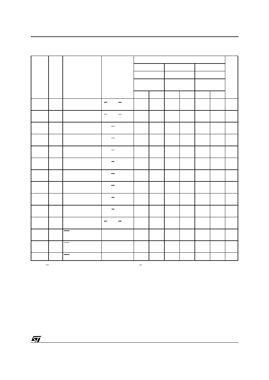
Symbol
Alt
Parameter
Test Condition
M29F002T / M29F002NT / M29F002B
Unit
-70
-90
-120
V
CC
= 5V
±
10% V
CC
= 5V
±
10% V
CC
= 5V
±
10%
Standard
Interface
Standard
Interface
Standard
Interface
Min
Max
Min
Max
Min
Max
t
AVAV
t
RC
Address Valid to
Next Address Valid
E = V
IL
, G = V
IL
70
90
120
ns
t
AVQV
t
ACC
Address Valid to
Output Valid
E = V
IL
, G = V
IL
70
90
120
ns
t
ELQX
(1)
t
LZ
Chip Enable Low to
Output Transition
G = V
IL
0
0
0
ns
t
ELQV
(2)
t
CE
Chip Enable Low to
Output Valid
G = V
IL
70
90
120
ns
t
GLQX
(1)
t
OLZ
Output Enable Low
to Output Transition
E = V
IL
0
0
0
ns
t
GLQV
(2)
t
OE
Output Enable Low
to Output Valid
E = V
IL
30
35
50
ns
t
EHQX
t
OH
Chip Enable High to
Output Transition
G = V
IL
0
0
0
ns
t
EHQZ
(1)
t
HZ
Chip Enable High to
Output Hi-Z
G = V
IL
20
20
30
ns
t
GHQX
t
OH
Output Enable High
to Output Transition
E = V
IL
0
0
0
ns
t
GHQZ
(1)
t
DF
Output Enable High
to Output Hi-Z
E = V
IL
20
20
30
ns
t
AXQX
t
OH
Address Transition
to Output Transition
E = V
IL
, G = V
IL
0
0
0
ns
t
PLEL
(1,3)
t
READY
RPNC Low to Read
Mode
10
10
10
µ
s
t
PHEL
t
RSP
RPNC High to Chip
Enable Low
50
50
50
ns
t
PLPX
t
RP
RPNC Pulse Width
500
500
500
ns
Notes: 1. Sampled only, not 100% tested.
2. G may be delayed by up to t
ELQV
- t
GLQV
after the falling edge of E without increasing t
ELQV
.
3. To be considered only if the Reset pulse is given while the memory is in Erase mode.
Table 14. Read AC Characteristics
(T
A
= 0 to 70
∞
C or ≠40 to 85
∞
C)
13/29
M29F002T, M29F002NT, M29F002B
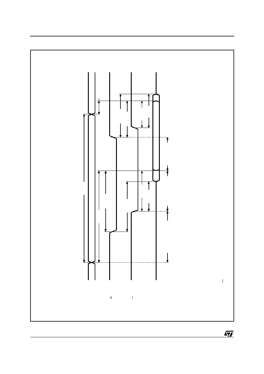
AI02082
tAVAV
tAVQV
tAXQX
tELQX
tEHQX
tGLQV
tGLQX
tGHQX
VALID
A0-A17
E
G
DQ0-DQ7
tELQV
VALID
ADDRESS
VALID
AND
CHIP
ENABLE
OUTPUT
ENABLE
DATA
VALID
tEHQZ
tGHQZ
Figure 6. Read Mode AC Waveforms
No
t
e
:
Wr
i
t
e
E
n
abl
e
(
W)
=
H
i
g
h
14/29
M29F002T, M29F002NT, M29F002B
Symbol
Alt
Parameter
M29F002T / M29F002NT / M29F002B
Unit
-70
-90
-120
V
CC
= 5V
±
10%
V
CC
= 5V
±
10% V
CC
= 5V
±
10%
Standard
Interface
Standard
Interface
Standard
Interface
Min
Max
Min
Max
Min
Max
t
AVAV
t
WC
Address Valid to Next Address
Valid
70
90
120
ns
t
ELWL
t
CS
Chip Enable Low to Write Enable
Low
0
0
0
ns
t
WLWH
t
WP
Write Enable Low to Write Enable
High
35
45
50
ns
t
DVWH
t
DS
Input Valid to Write Enable High
30
45
50
ns
t
WHDX
t
DH
Write Enable High to Input
Transition
0
0
0
ns
t
WHEH
t
CH
Write Enable High to Chip Enable
High
0
0
0
ns
t
WHWL
t
WPH
Write Enable High to Write Enable
Low
20
20
20
ns
t
AVWL
t
AS
Address Valid to Write Enable Low
5
5
5
ns
t
WLAX
t
AH
Write Enable Low to Address
Transition
45
45
50
ns
t
GHWL
Output Enable High to Write
Enable Low
0
0
0
ns
t
VCHEL
t
VCS
V
CC
High to Chip Enable Low
50
50
50
µ
s
t
WHGL
t
OEH
Write Enable High to Output
Enable Low
0
0
0
ns
t
PHPHH
(1,2)
t
VIDR
RPNC Rise Time to V
ID
500
500
500
ns
t
PLPX
t
RP
RPNC Pulse Width
500
500
500
ns
Notes: 1. Sample only, not 100% tested.
2. This timing is for Temporary Block Unprotection operation.
Table 15. Write AC Characteristics, Write Enable Controlled
(T
A
= 0 to 70
∞
C or ≠40 to 85
∞
C)
Chip Erase (CE) Instruction. This instruction uses
six write cycles. The Erase Set-up command 80h
is written to address 555h on the third cycle after
the two Coded cycles. The Chip Erase Confirm
command 10h is similarly written on the sixth cycle
after another two Coded cycles. If the second
command given is not an erase confirm or if the
Coded cycles are wrong, the instruction aborts and
the device is reset to Read Array. It is not necessary
to program the array with 00h first as the P/E.C. will
automatically do this before erasing it to FFh. Read
operations after the sixth rising edge of W or E
output the Status Register bits. During the execu-
tion of theerase by the P/E.C.,Data Polling bit DQ7
returns '0', then '1' on completion. The Toggle bits
DQ2 and DQ6 toggle during erase operation and
stop when erase is completed. After completionthe
Status Register bit DQ5 returns '1' if there has been
an Erase Failure.
15/29
M29F002T, M29F002NT, M29F002B
AI02083
E
G
W
A0-A17
DQ0-DQ7
VALID
VALID
VCC
tVCHEL
tWHEH
tWHWL
tELWL
tAVWL
tWHGL
tWLAX
tWHDX
tAVAV
tDVWH
tWLWH
tGHWL
Figure 7. Write AC Waveforms, W Controlled
Note: Address are latched on the falling edge of W, Data is latched on the rising edge of W.
Erase Suspend (ES) Instruction. The Block
Erase operation may be suspended by this instruc-
tion which consists of writing the command B0h
without any specific address. No Coded cycles are
required. It permits reading of data from another
block and programming in another block while an
erase operation is in progress. Erase suspend is
accepted only during the Block Erase instruction
execution. Writing this command during Erase
timeout will, in addition to suspending the erase,
terminate the timeout. The Toggle bit DQ6 stops
togglingwhen the P/E.C. is suspended.The Toggle
bits will stop toggling between 0.1
µ
s and 15
µ
s after
the Erase Suspend (ES) command has been writ-
ten. The device will then automatically be set to
Read Memory Array mode. When erase is sus-
pended, a Read from blocks being erased will
output DQ2 toggling and DQ6 at '1'. A Read from
a block not being erased returns valid data. During
suspension the memory will respond only to the
Erase Resume ER and the Program PG instruc-
tions. A Program operation can be initiated during
erase suspend in one of the blocks not being
erased. It will result in both DQ2 and DQ6 toggling
when the data is beingprogrammed. ARead/Reset
command will definitively abort erasure and result
in invalid data in the blocks being erased.
Erase Resume (ER) Instruction. If an Erase Sus-
pend instruction was previously executed, the
erase operation may be resumed by giving the
command 30h, at any address, and without any
Coded cycles.
POWER SUPPLY
Power Up
The memory Command Interface is reset on power
up to Read Array. Either E or W must be tied to V
IH
during Power Up to allow maximum security and
the possibility to write a command on the first rising
edge of E and W. Any write cycle initiation is
blocked when Vcc is below V
LKO
.
Supply Rails
Normal precautions must be taken for supply volt-
age decoupling; each device in a system should
have the V
CC
rail decoupledwith a 0.1
µ
F capacitor
close to the V
CC
and V
SS
pins. The PCB trace
widths should be sufficient to carry the V
CC
pro-
gram and erase currents required.
16/29
M29F002T, M29F002NT, M29F002B
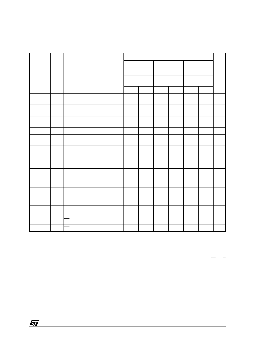
Symbol
Alt
Parameter
M29F002T / M29F002NT / M29F002B
Unit
-70
-90
-120
V
CC
= 5V
±
10%
V
CC
= 5V
±
10%
V
CC
= 5V
±
10%
Standard
Interface
Standard
Interface
Standard
Interface
Min
Max
Min
Max
Min
Max
t
AVAV
t
WC
Address Valid to Next Address
Valid
70
90
120
ns
t
WLEL
t
WS
Write Enable Low to Chip
Enable Low
0
0
0
ns
t
ELEH
t
CP
Chip Enable Low to Chip
Enable High
35
45
50
ns
t
DVEH
t
DS
Input Valid to Chip Enable High
30
45
50
ns
t
EHDX
t
DH
Chip Enable High to Input
Transition
5
5
5
ns
t
EHWH
t
WH
Chip Enable High to Write
Enable High
0
0
0
ns
t
EHEL
t
CPH
Chip Enable High to Chip
Enable Low
20
20
20
ns
t
AVEL
t
AS
Address Valid to Chip Enable
Low
0
0
0
ns
t
ELAX
t
AH
Chip Enable Low to Address
Transition
45
45
50
ns
t
GHEL
Output Enable High Chip
Enable Low
0
0
0
ns
t
VCHWL
t
VCS
V
CC
High to Write Enable Low
50
50
50
µ
s
t
EHGL
t
OEH
Chip Enable High to Output
Enable Low
0
0
0
ns
t
PHPHH
(1,2)
t
VIDR
RPNC Rise TIme to V
ID
500
500
500
ns
t
PLPX
t
RP
RPNC Pulse Width
500
500
500
ns
Notes: 1. Sample only, not 100% tested.
2. This timing is for Temporary Block Unprotection operation.
Table 16. Write AC Characteristics, Chip Enable Controlled
(T
A
= 0 to 70
∞
C or ≠40 to 85
∞
C)
17/29
M29F002T, M29F002NT, M29F002B
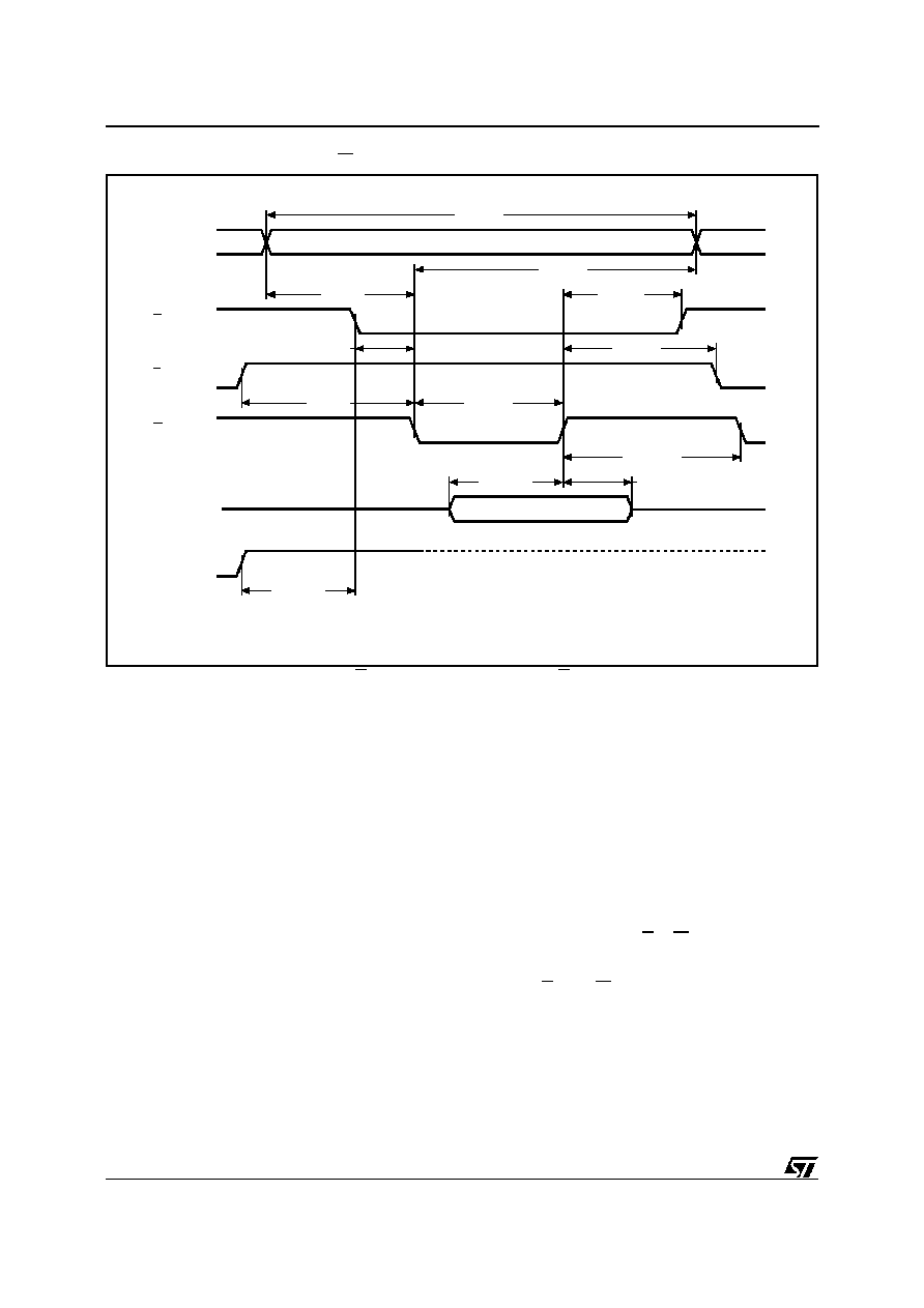
AI02084
E
G
W
A0-A17
DQ0-DQ7
VALID
VALID
VCC
tVCHWL
tEHWH
tEHEL
tWLEL
tAVEL
tEHGL
tELAX
tEHDX
tAVAV
tDVEH
tELEH
tGHEL
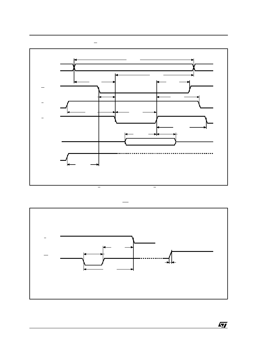
Figure 8. Write AC Waveforms, E Controlled
Note: Address are latched on the falling edge of E, Data is latched on the rising edge of E.
AI02085
E
RPNC
tPLPX
tPHEL
tPLEL
tPHPHH
Figure 9. Read and Write AC Characteristics, RP Related
18/29
M29F002T, M29F002NT, M29F002B
Sym-
bol
Alt
Parameter
M29F002T / M29F002NT / M29F002B
Unit
-70
-90
-120
V
CC
= 5V
±
10%
V
CC
= 5V
±
10%
V
CC
= 5V
±
10%
Standard
Interface
Standard
Interface
Standard
Interface
Min
Max
Min
Max
Min
Max
t
WHQ7V
Write Enable High to DQ7 Valid
(Program, W Controlled)
10
2400
10
2400
10
2400
µ
s
Write Enable High to DQ7 Valid
(Chip Erase, W Controlled)
1.0
30
1.0
30
1.0
30
sec
t
EHQ7V
Chip Enable High to DQ7 Valid
(Program, E Controlled)
10
2400
10
2400
10
2400
µ
s
Chip Enable High to DQ7 Valid
(Chip Erase, E Controlled)
1.0
30
1.0
30
1.0
30
sec
t
Q7VQV
Q7 Valid to Output Valid (Data
Polling)
30
35
50
ns
t
WHQV
Write Enable High to Output
Valid (Program)
10
2400
10
2400
10
2400
µ
s
Write Enable High to Output
Valid (Chip Erase)
1.0
30
1.0
30
1.0
30
sec
t
EHQV
Chip Enable High to Output
Valid (Program)
10
2400
10
2400
10
2400
µ
s
Chip Enable High to Output
Valid (Chip Erase)
1.0
30
1.0
30
1.0
30
sec
Note: 1. All other timings are defined in Read AC Characteristics table.
Table 17. Data Polling and Toggle Bit AC Characteristics
(1)
(T
A
= 0 to 70
∞
C or ≠40 to 85
∞
C)
19/29
M29F002T, M29F002NT, M29F002B
AI02086
E
G
W
A0-A17
DQ7
IGNORE
VALID
DQ0-DQ6
ADDRESS
(WITHIN
BLOCKS)
DATA
OUTPUT
VALID
tAVQV
tEHQ7V
tGLQV
tWHQ7V
VALID
tQ7VQV
DQ7
DATA
POLLING
(LAST)
CYCLE
MEMORY
ARRAY
READ
CYCLE
DATA
POLLING
READ
CYCLES
LAST
WRITE
CYCLE
OF
PROGRAM
OR
ERASE
INSTRUCTION
tELQV
Figure 10. Data Polling DQ7 AC Waveforms
20/29
M29F002T, M29F002NT, M29F002B
READ DQ5 & DQ7
at VALID ADDRESS
START
READ DQ7
FAIL
PASS
AI01369
DQ7
=
DATA
YES
NO
YES
NO
DQ5
= 1
DQ7
=
DATA
YES
NO
Figure 11. Data Polling Flowchart
READ
DQ2, DQ5 & DQ6
START
READ DQ2, DQ6
FAIL
PASS
AI01873
DQ2, DQ6
=
TOGGLE
NO
NO
YES
YES
DQ5
= 1
NO
YES
DQ2, DQ6
=
TOGGLE
Figure 12. Data Toggle Flowchart
Parameter
M29F002T / M29F002NT / M29F002B
Unit
Min
Typ
Typical after
100k W/E Cycles
Chip Erase (Preprogrammed)
0.7
0.9
sec
Chip Erase
2.4
2.5
sec
Boot Block Erase
0.6
sec
Parameter Block Erase
0.5
sec
Main Block (32Kb) Erase
0.9
sec
Main Block (64Kb) Erase
1.0
sec
Chip Program (Byte)
3.2
3.2
sec
Byte Program
11
11
µ
s
Program/Erase Cycles (per Block)
100,000
cycles
Table 18. Program, Erase Times and Program, Erase Endurance Cycles
(T
A
= 0 to 70
∞
C)
21/29
M29F002T, M29F002NT, M29F002B
AI02087
E
G
W
A0-A17
DQ6,DQ2
tAVQV
STOP
TOGGLE
LAST
WRITE
CYCLE
OF
PROGRAM
OF
ERASE
INSTRUCTION
VALID
VALID
VALID
IGNORE
DATA
TOGGLE
READ
CYCLE
MEMORY
ARRAY
READ
CYCLE
tWHQV
tEHQV
tELQV
tGLQV
DATA
TOGGLE
READ
CYCLE
DQ0-DQ1,DQ3-DQ5,DQ7
Figure 13. Data Toggle DQ6, DQ2 AC Waveforms
No
t
e
:
A
l
l
o
t
h
e
r
t
i
m
i
ng
s
a
r
e
as
a
nor
m
a
l
R
ea
d
c
y
c
l
e
.
22/29
M29F002T, M29F002NT, M29F002B
BLOCK ADDRESS
on A13-A17
AI02088B
G, A9 = VID,
E = VIL
n = 0
Wait 4
µ
s
Wait 100
µ
s
W = VIL
W = VIH
E, G = VIH
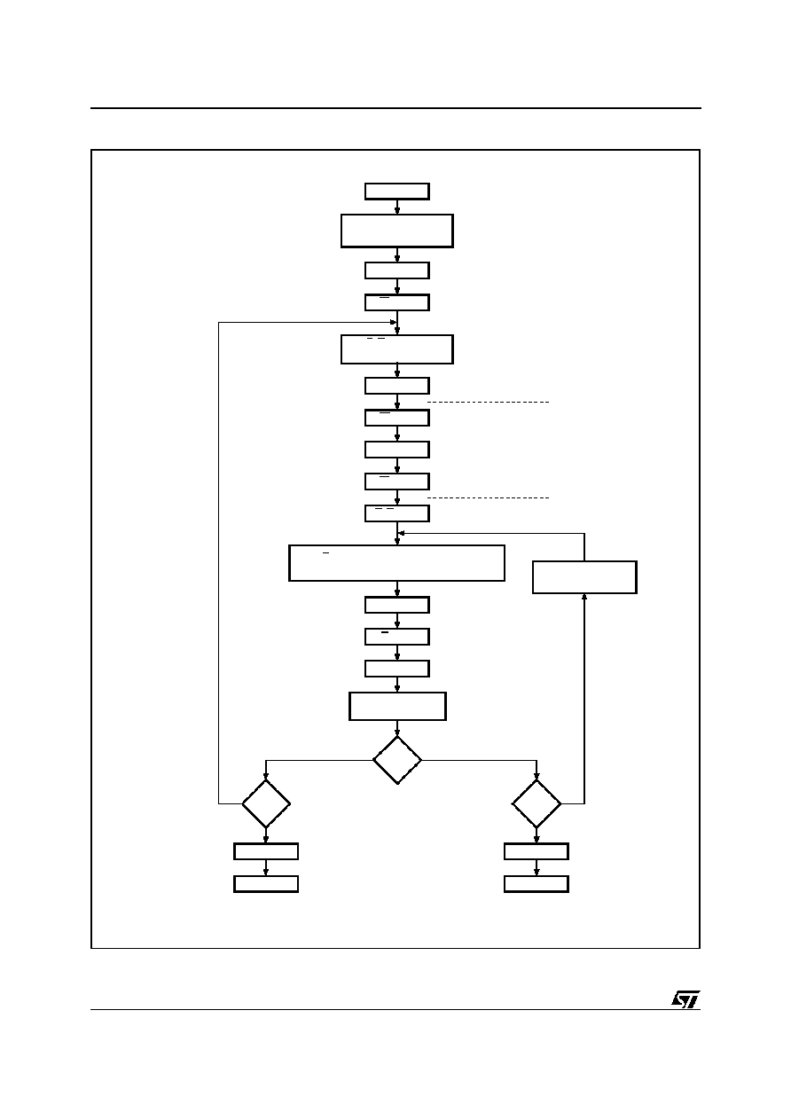
VERIFY BLOCK PROTECTION
A0, A6 = VIL; A1 = VIH; A9 = VID
A13-A17 IDENTIFY BLOCK
A9 = VIH
++n
= 25
START
FAIL
PASS
YES
NO
DATA
=
01h
YES
NO
A9 = VIH
Set-up
Protect
Verify
W = VIH
Wait 4
µ
s
Wait 60ns
G = VIL
VERIFY BLOCK
PROTECT STATUS
E = VIL
Figure 14. Block Protection Flowchart
23/29
M29F002T, M29F002NT, M29F002B
PROTECT
ALL BLOCKS
AI02089C
DATA
E, G, A9 = VID
A12, A15 = VIH
Wait 4
µ
s
W = VIH
E, G = VIH
Wait 10ms
=
00h
NEXT
BLOCK
W = VIL
++n
= 1000
START
A9 = VIH
YES
YES
NO
A9 = VIH
NO
LAST
BLK.
YES
NO
n = 0
Set-up
Unprotect
Verify
W = VIH
E, A0 = VIL; A1, A6 = VIH; A9 = VID
A13-A17 IDENTIFY BLOCK
Wait 4
µ
s
Wait 60ns
G = VIL
VERIFY BLOCK
PROTECT STATUS
FAIL
PASS
Figure 15. All Blocks Unprotecting Flowchart
24/29
M29F002T, M29F002NT, M29F002B
ORDERING INFORMATION SCHEME
Devices are shipped from the factory with the memory content erased (to FFh).
For a list of available options (Speed, Package, etc...) or for further informationon any aspect of this device,
please contact the STMicroelectronics Sales Office nearest to you.
Operating Voltage
F
5V
Array Matrix
T
Top Boot
B
Bottom Boot
NT
Top Boot
without
RPNC function
Speed
-70
70ns
-90
90ns
-120 120ns
Power Supplies
blank V
CC
±
10%
X
V
CC
±
5%
Package
P
PDIP32
K
PLCC32
N
TSOP32
(8 x 20 mm)
Option
TR
Tape & Reel
Packing
Temp. Range
1
0 to 70
∞
C
6
≠40 to 85
∞
C
Example:
M29F002T
-70
X
K
1
TR
25/29
M29F002T, M29F002NT, M29F002B
PDIP
A2
A1
A
L
B1
B
e1
D
S
E1
E
N
1
C
eA
eB
D2
Symb
mm
inches
Typ
Min
Max
Typ
Min
Max
A
≠
5.08
≠
0.200
A1
0.38
≠
0.015
≠
A2
3.56
4.06
0.140
0.160
B
0.38
0.51
0.015
0.020
B1
1.52
≠
≠
0.060
≠
≠
C
0.20
0.30
0.008
0.012
D
41.78
42.04
1.645
1.655
D2
38.10
≠
≠
1.500
≠
≠
E
15.24
≠
≠
0.600
≠
≠
E1
13.59
13.84
0.535
0.545
e1
2.54
≠
≠
0.100
≠
≠
eA
15.24
≠
≠
0.600
≠
≠
eB
15.24
17.78
0.600
0.700
L
3.18
3.43
0.125
0.135
S
1.78
2.03
0.070
0.080
0
∞
10
∞
0
∞
10
∞
N
32
32
Drawing is not to scale.
PDIP32 - 32 pin Plastic DIP, 600 mils width
26/29
M29F002T, M29F002NT, M29F002B
PLCC
D
Ne
E1 E
1 N
D1
Nd
CP
B
D2/E2
e
B1
A1
A
R
0.51 (.020)
1.14 (.045)
F
A2
Symb
mm
inches
Typ
Min
Max
Typ
Min
Max
A
2.54
3.56
0.100
0.140
A1
1.52
2.41
0.060
0.095
A2
≠
0.38
≠
0.015
B
0.33
0.53
0.013
0.021
B1
0.66
0.81
0.026
0.032
D
12.32
12.57
0.485
0.495
D1
11.35
11.56
0.447
0.455
D2
9.91
10.92
0.390
0.430
E
14.86
15.11
0.585
0.595
E1
13.89
14.10
0.547
0.555
E2
12.45
13.46
0.490
0.530
e
1.27
≠
≠
0.050
≠
≠
F
0.00
0.25
0.000
0.010
R
0.89
≠
≠
0.035
≠
≠
N
32
32
Nd
7
7
Ne
9
9
CP
0.10
0.004
Drawing is not to scale.
PLCC32 - 32 lead Plastic Leaded Chip Carrier, rectangular
27/29
M29F002T, M29F002NT, M29F002B
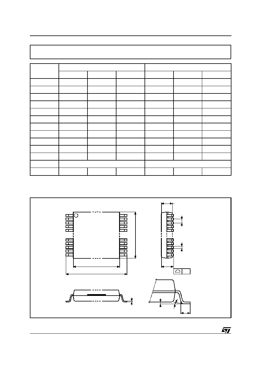
TSOP32 - 32 lead Plastic Thin Small Outline, 8 x 20mm
TSOP-a
D1
E
1
N
CP
B
e
A2
A
N/2
D
DIE
C
L
A1
Symb
mm
inches
Typ
Min
Max
Typ
Min
Max
A
1.20
0.047
A1
0.05
0.15
0.002
0.007
A2
0.95
1.05
0.037
0.041
B
0.15
0.27
0.006
0.011
C
0.10
0.21
0.004
0.008
D
19.80
20.20
0.780
0.795
D1
18.30
18.50
0.720
0.728
E
7.90
8.10
0.311
0.319
e
0.50
-
-
0.020
-
-
L
0.50
0.70
0.020
0.028
0
∞
5
∞
0
∞
5
∞
N
32
32
CP
0.10
0.004
Drawing is not to scale.
28/29
M29F002T, M29F002NT, M29F002B

Information furnished is believed to be accurate and reliable. However, STMicroelectronics assumes no responsibility for the consequences
of use of such information nor for any infringement of patents or other rights of third parties which may result from its use. No license is granted
by implication or otherwise under any patent or patent rights of STMicroelectronics. Spec ifications mentioned in this publication are subject to
change without notice. This publication supersedes and replaces all information previously supplied. STMicroelectronics products are not
authorized for use as critical components in life support devices or systems without express written approval of STMicroelectronics.
The ST logo is a registered trademark of STMicroelectronics.
©
1998 STMicroelectronics - All Rights Reserved
STMicroelectronics GROUP OF COMPANIES
Australia - Brazil - Canada - China - France - Germany - Italy - Japan - Korea - Malaysia - Malta - Mexico - Morocco - The Netherlands -
Singapore - Spain - Sweden - Switzerland - Taiwan - Thailand - United Kingdom - U.S.A.
29/29
M29F002T, M29F002NT, M29F002B