
1/21
PRELIMINARY DATA
September 1999
This is preliminary information on a new product now in development or undergoing evaluation. Details are subject to change without notice.
M29F040B
4 Mbit (512Kb x8, Uniform Block) Single Supply Flash Memory
s
SINGLE 5V
±
10% SUPPLY VOLTAGE for
PROGRAM, ERASE and READ OPERATIONS
s
ACCESS TIME: 45ns
s
PROGRAMMING TIME
≠ 8
µ
s per Byte typical
s
8 UNIFORM 64 Kbytes MEMORY BLOCKS
s
PROGRAM/ERASE CONTROLLER
≠ Embedded Byte Program algorithm
≠ Embedded Multi-Block/Chip Erase algorithm
≠ Status Register Polling and Toggle Bits
s
ERASE SUSPEND and RESUME MODES
≠ Read and Program another Block during
Erase Suspend
s
UNLOCK BYPASS PROGRAM COMMAND
≠ Faster Production/Batch Programming
s
LOW POWER CONSUMPTION
≠ Standby and Automatic Standby
s
100,000 PROGRAM/ERASE CYCLES per
BLOCK
s
20 YEARS DATA RETENTION
≠ Defectivity below 1 ppm/year
s
ELECTRONIC SIGNATURE
≠ Manufacturer Code: 20h
≠ Device Code: E2h
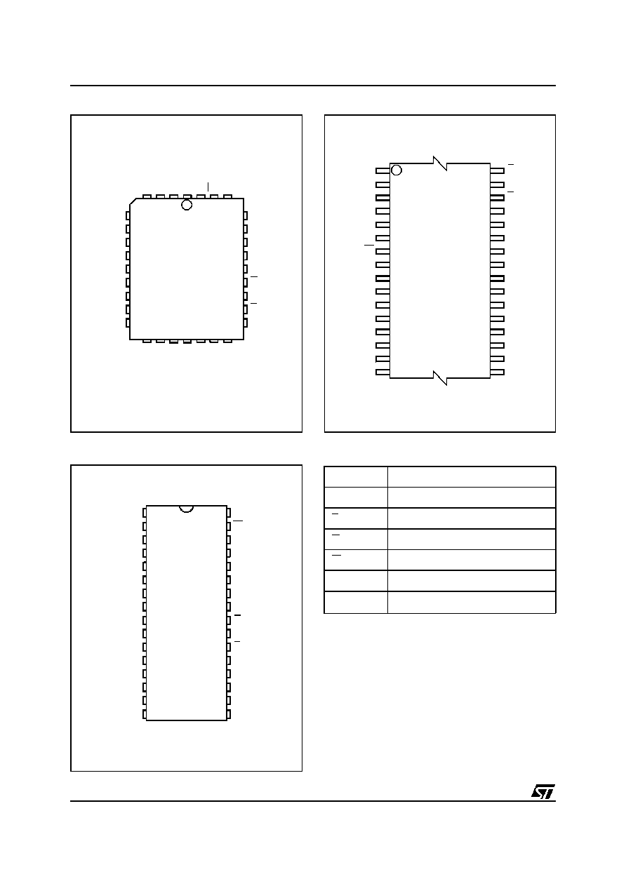
32
1
TSOP32 (N)
8 x 20mm
PLCC32 (K)
PDIP32 (P)
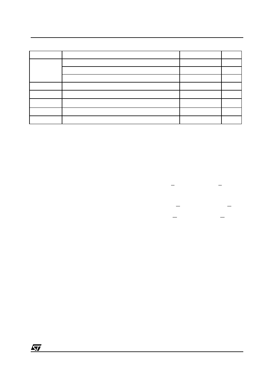
Figure 1. Logic Diagram
AI02900
19
A0-A18
W
DQ0-DQ7
VCC
M29F040B
G
E
VSS
8
M29F040B
2/21
Figure 2A. PLCC Connections
AI02901
A17
A13
A10
DQ5
17
A1
A0
DQ0
DQ1
DQ2
DQ3
DQ4
A7
A4
A3
A2
A6
A5
9
W
A8
1
A16
A9
DQ7
A12
A14
32
A18
V
CC
M29F040B
A15
A11
DQ6
G
E
25
V
SS
Figure 2B. TSOP Connections
A1
A0
DQ0
A7
A4
A3
A2
A6
A5
A13
A10
A8
A9
DQ7
A14
A11
G
E
DQ5
DQ1
DQ2
DQ3
DQ4
DQ6
A17
W
A16
A12
A18
VCC
A15
AI02902
M29F040B
8
1
9
16
17
24
25
32
VSS
Figure 2C. PDIP Connections
A1
A0
DQ0
A7
A4
A3
A2
A6
A5
A13
A10
A8
A9
DQ7
A14
A11
G
E
DQ5
DQ1
DQ2
DQ3
VSS
DQ4
DQ6
A17
W
A16
A12
A18
VCC
A15
AI02910
M29F040B
8
1
2
3
4
5
6
7
9
10
11
12
13
14
15
16
32
31
30
29
28
27
26
25
24
23
22
21
20
19
18
17
Table 1. Signal Names
A0-A18
Address Inputs
DQ0-DQ7
Data Inputs/Outputs
E
Chip Enable
G
Output Enable
W
Write Enable
V
CC
Supply Voltage
V
SS
Ground
SUMMARY DESCRIPTION
The M29F040B is a 4 Mbit (512Kb x8) non-volatile
memory that can be read, erased and repro-
grammed. These operations can be performed us-
ing a single 5V supply. On power-up the memory
defaults to its Read mode where it can be read in
the same way as a ROM or EPROM. The
M29F040B is fully backward compatible with the
M29F040.
The memory is divided into blocks that can be
erased independently so it is possible to preserve
3/21
M29F040B
valid data while old data is erased. Each block can
be protected independently to prevent accidental
Program or Erase commands from modifying the
memory. Program and Erase commands are writ-
ten to the Command Interface of the memory. An
on-chip Program/Erase Controller simplifies the
process of programming or erasing the memory by
taking care of all of the special operations that are
required to update the memory contents. The end
of a program or erase operation can be detected
and any error conditions identified. The command
set required to control the memory is consistent
with JEDEC standards.
Chip Enable, Output Enable and Write Enable sig-
nals control the bus operation of the memory.
They allow simple connection to most micropro-
cessors, often without additional logic.
The memory is offered in TSOP32 (8 x 20mm),
PLCC32 and PDIP32 packages. Access times of
45ns, 55ns, 70ns and 90ns are available. The
memory is supplied with all the bits erased (set to
`1').
SIGNAL DESCRIPTIONS
See Figure 1, Logic Diagram, and Table 1, Signal
Names, for a brief overview of the signals connect-
ed to this device.
Address Inputs (A0-A18). The Address Inputs
select the cells in the memory array to access dur-
ing Bus Read operations. During Bus Write opera-
tions they control the commands sent to the
Command Interface of the internal state machine.
Data Inputs/Outputs (DQ0-DQ7). The Data In-
puts/Outputs output the data stored at the selected
address during a Bus Read operation. During Bus
Write operations they represent the commands
sent to the Command Interface of the internal state
machine.
Chip Enable (E). The Chip Enable, E, activates
the memory, allowing Bus Read and Bus Write op-
erations to be performed. When Chip Enable is
High, V
IH
, all other pins are ignored.
Output Enable (G). The Output Enable, G, con-
trols the Bus Read operation of the memory.
Write Enable (W). The Write Enable, W, controls
the Bus Write operation of the memory's Com-
mand Interface.
V
CC
Supply Voltage. The V
CC
Supply Voltage
supplies the power for all operations (Read, Pro-
gram, Erase etc.).
The Command Interface is disabled when the V
CC
Supply Voltage is less than the Lockout Voltage,
V
LKO
. This prevents Bus Write operations from ac-
cidentally damaging the data during power up,
power down and power surges. If the Program/
Erase Controller is programming or erasing during
this time then the operation aborts and the memo-
ry contents being altered will be invalid.
A 0.1
µ
F capacitor should be connected between
the V
CC
Supply Voltage pin and the V
SS
Ground
pin to decouple the current surges from the power
supply. The PCB track widths must be sufficient to
carry the currents required during program and
erase operations, I
CC4
.
V
SS
Ground. The V
SS
Ground is the reference for
all voltage measurements.
Table 2. Absolute Maximum Ratings
(1)
Note: 1. Except for the rating "Operating Temperature Range", stresses above those listed in the Table "Absolute Maximum Ratings" may
cause permanent damage to the device. These are stress ratings only and operation of the device at these or any other conditions
above those indicated in the Operating sections of this specification is not implied. Exposure to Absolute Maximum Rating condi-
tions for extended periods may affect device reliability. Refer also to the STMicroelectronics SURE Program and other relevant qual-
ity documents.
2. Minimum Voltage may undershoot to ≠2V during transition and for less than 20ns during transitions.
Symbol
Parameter
Value
Unit
T
A
Ambient Operating Temperature (Temperature Range Option 1)
0 to 70
∞
C
Ambient Operating Temperature (Temperature Range Option 6)
≠40 to 85
∞
C
Ambient Operating Temperature (Temperature Range Option 3)
≠40 to 125
∞
C
T
BIAS
Temperature Under Bias
≠50 to 125
∞
C
T
STG
Storage Temperature
≠65 to 150
∞
C
V
IO
(2)
Input or Output Voltage
≠0.6 to 6
V
V
CC
Supply Voltage
≠0.6 to 6
V
V
ID
Identification Voltage
≠0.6 to 13.5
V

M29F040B
4/21
Table 3. Block Addresses
Size (Kbytes)
Address Range
64
70000h-7FFFFh
64
60000h-6FFFFh
64
50000h-5FFFFh
64
40000h-4FFFFh
64
30000h-3FFFFh
64
20000h-2FFFFh
64
10000h-1FFFFh
64
00000h-0FFFFh
BUS OPERATIONS
There are five standard bus operations that control
the device. These are Bus Read, Bus Write, Out-
put Disable, Standby and Automatic Standby. See
Table 4, Bus Operations, for a summary. Typically
glitches of less than 5ns on Chip Enable or Write
Enable are ignored by the memory and do not af-
fect bus operations.
Bus Read. Bus Read operations read from the
memory cells, or specific registers in the Com-
mand Interface. A valid Bus Read operation in-
volves setting the desired address on the Address
Inputs, applying a Low signal, V
IL
, to Chip Enable
and Output Enable and keeping Write Enable
High, V
IH
. The Data Inputs/Outputs will output the
value, see Figure 7, Read Mode AC Waveforms,
and Table 11, Read AC Characteristics, for details
of when the output becomes valid.
Bus Write. Bus Write operations write to the
Command Interface. A valid Bus Write operation
begins by setting the desired address on the Ad-
dress Inputs. The Address Inputs are latched by
the Command Interface on the falling edge of Chip
Enable or Write Enable, whichever occurs last.
The Data Inputs/Outputs are latched by the Com-
mand Interface on the rising edge of Chip Enable
or Write Enable, whichever occurs first. Output En-
able must remain High, V
IH
, during the whole Bus
Write operation. See Figures 8 and 9, Write AC
Waveforms, and Tables 12 and 13, Write AC
Characteristics, for details of the timing require-
ments.
Output Disable. The Data Inputs/Outputs are in
the high impedance state when Output Enable is
High, V
IH
.
Standby. When Chip Enable is High, V
IH
, the
Data Inputs/Outputs pins are placed in the high-
impedance state and the Supply Current is re-
duced to the Standby level.
When Chip Enable is at V
IH
the Supply Current is
reduced to the TTL Standby Supply Current, I
CC2
.
To further reduce the Supply Current to the CMOS
Standby Supply Current, I
CC3
, Chip Enable should
be held within V
CC
±
0.2V. For Standby current
levels see Table 10, DC Characteristics.
During program or erase operations the memory
will continue to use the Program/Erase Supply
Current, I
CC4
, for Program or Erase operations un-
til the operation completes.
5/21
M29F040B
Table 4. Bus Operations
Note: X = V
IL
or V
IH
.
Operation
E
G
W
Address Inpu ts
Data
Inputs/Outpu ts
Bus Read
V
IL
V
IL
V
IH
Cell Address
Data Output
Bus Write
V
IL
V
IH
V
IL
Command Address
Data Input
Output Disable
X
V
IH
V
IH
X
Hi-Z
Standby
V
IH
X
X
X
Hi-Z
Read Manufacturer
Code
V
IL
V
IL
V
IH
A0 = V
IL
, A1 = V
IL
, A9 = V
ID
,
Others V
IL
or V
IH
20h
Read Device Code
V
IL
V
IL
V
IH
A0 = V
IH
, A1 = V
IL
, A9 = V
ID
,
Others V
IL
or V
IH
E2h
Automatic Standby. If CMOS levels (V
CC
±
0.2V)
are used to drive the bus and the bus is inactive for
150ns or more the memory enters Automatic
Standby where the internal Supply Current is re-
duced to the CMOS Standby Supply Current, I
CC3
.
The Data Inputs/Outputs will still output data if a
Bus Read operation is in progress.
Special Bus Operations
Additional bus operations can be performed to
read the Electronic Signature and also to apply
and remove Block Protection. These bus opera-
tions are intended for use by programming equip-
ment and are not usually used in applications.
They require V
ID
to be applied to some pins.
Electronic Signature. The
memory
has
two
codes, the manufacturer code and the device
code, that can be read to identify the memory.
These codes can be read by applying the signals
listed in Table 4, Bus Operations.
Block Protection and Blocks Unprotection. Each
block can be separately protected against acci-
dental Program or Erase. Protected blocks can be
unprotected to allow data to be changed. Block
Protection and Blocks Unprotection operations
must only be performed on programming equip-
ment. For further information refer to Application
Note AN1122, Applying Protection and Unprotec-
tion to M29 Series Flash.