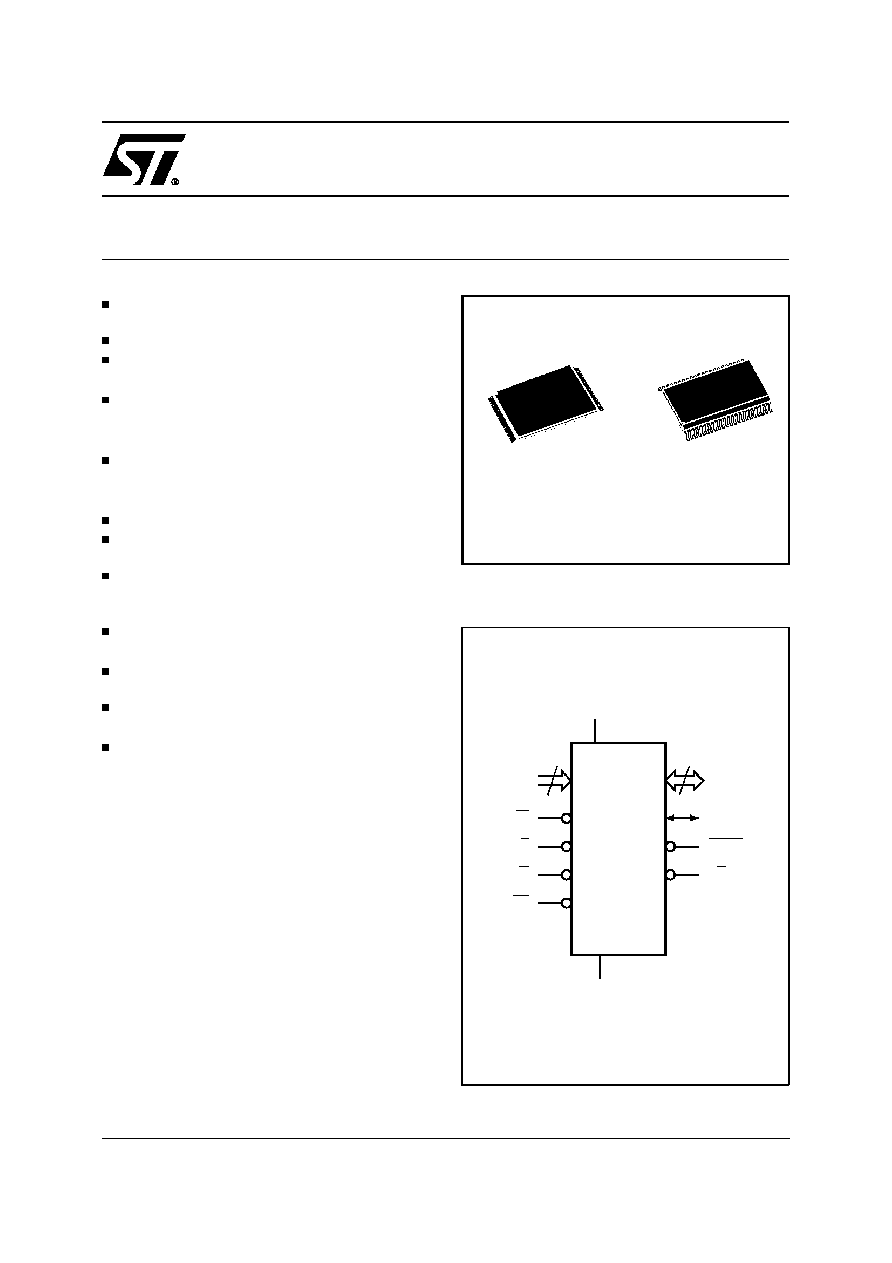
AI01986
17
A0-A16
W
DQ0-DQ14
VCC
M29F200T
M29F200B
E
VSS
15
G
RP
DQ15A≠1
BYTE
RB
Figure 1. Logic Diagram
M29F200T
M29F200B
2 Mbit (256Kb x8 or 128Kb x16, Boot Block)
Single Supply Flash Memory
5V
±
10% SUPPLY VOLTAGE for PROGRAM,
ERASE and READ OPERATIONS
FAST ACCESS TIME: 55ns
FAST PROGRAMMING TIME
≠ 10
µ
s by Byte / 16
µ
s by Word typical
PROGRAM/ERASE CONTROLLER (P/E.C.)
≠ Program Byte-by-Byte or Word-by-Word
≠ Status Register bits and Ready/Busy Output
MEMORY BLOCKS
≠ Boot Block (Top or Bottom location)
≠ Parameter and Main blocks
BLOCK, MULTI-BLOCK and CHIP ERASE
MULTI-BLOCK PROTECTION/TEMPORARY
UNPROTECTION MODES
ERASE SUSPEND and RESUME MODES
≠ Read and Program another Block during
Erase Suspend
LOW POWER CONSUMPTION
≠ Stand-by and Automatic Stand-by
100,000 PROGRAM/ERASE CYCLES per
BLOCK
20 YEARS DATA RETENTION
≠ Defectivity below 1ppm/year
ELECTRONIC SIGNATURE
≠ Manufacturer Code: 0020h
≠ Device Code, M29F200T: 00D3h
≠ Device Code, M29F200B: 00D4h
DESCRIPTION
The M29F200 is a non-volatile memory that may
be erased electrically at the block or chip level and
programmed in-system on a Byte-by-Byteor Word-
by-Word basis using only a single 5V V
CC
supply.
For Program and Erase operations the necessary
high voltages are generated internally. The device
can also be programmed in standard program-
mers.
The array matrix organisation allows each block to
be erased and reprogrammed without affecting
other blocks. Blocks can be protected against pro-
graming and erase on programming equipment,
and temporarily unprotected to make changes in
the application.
July 1998
1/33
44
1
SO44 (M)
TSOP48 (N)
12 x 20 mm
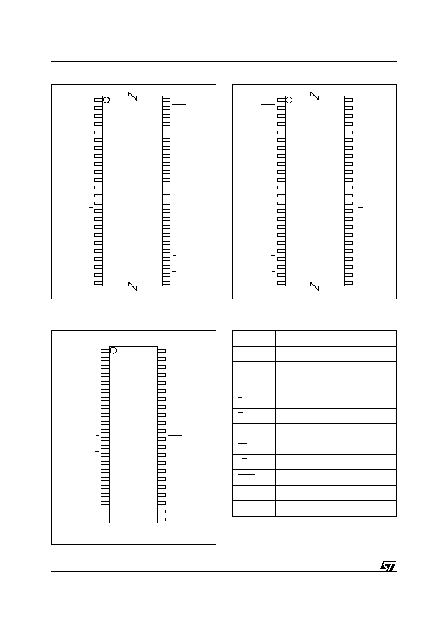
DQ3
DQ9
DQ2
A6
DQ0
W
A3
RB
DQ6
A8
A9
DQ13
NC
A10
DQ14
A2
DQ12
DQ10
DQ15A≠1
VCC
DQ4
DQ5
A7
DQ7
NC
NC
AI01987
M29F200T
M29F200B
(Normal)
12
1
13
24
25
36
37
48
DQ8
NC
NC
A1
NC
A4
A5
DQ1
DQ11
G
A12
A13
A16
A11
BYTE
A15
A14
VSS
E
A0
RP
VSS
Figure 2A. TSOP Pin Connections
G
DQ0
DQ8
A3
A0
E
VSS
A2
A1
A13
VSS
A14
A15
DQ7
A12
A16
BYTE
DQ15A≠1
DQ5
DQ2
DQ3
VCC
DQ11
DQ4
DQ14
A9
W
RB
A4
NC
RP
A7
AI01989
M29F200T
M29F200B
8
2
3
4
5
6
7
9
10
11
12
13
14
15
16
32
31
30
29
28
27
26
25
24
23
22
20
19
18
17
DQ1
DQ9
A6
A5
DQ6
DQ13
44
39
38
37
36
35
34
33
A11
A10
DQ10
21
DQ12
40
43
1
42
41
NC
A8
Figure 2C. SO Pin Connections
DQ3
DQ9
DQ2
DQ0
DQ6
DQ13
DQ14
DQ12
DQ10
DQ15A≠1
VCC
DQ4
DQ5
DQ7
AI01988
M29F200T
M29F200B
(Reverse)
12
1
13
24
25
36
37
48
DQ8
DQ1
DQ11
A16
BYTE
VSS
A0
VSS
A6
A3
A8
A9
NC
A10
A2
A7
NC
NC
NC
NC
A1
NC
A4
A5
A12
A13
A11
A15
A14
RP
W
RB
G
E
Figure 2B. TSOP Reverse Pin Connections
A0-A16
Address Inputs
DQ0-DQ7
Data Input/Outputs, Command Inputs
DQ8-DQ14
Data Input/Outputs
DQ15A≠1
Data Input/Output or Address Input
E
Chip Enable
G
Output Enable
W
Write Enable
RP
Reset / Block Temporary Unprotect
RB
Ready/Busy Output
BYTE
Byte/Word Organisation
V
CC
Supply Voltage
V
SS
Ground
Table 1. Signal Names
Warning: NC = Not Connected.
Warning: NC = Not Connected.
Warning: NC = Not Connected.
2/33
M29F200T, M29F200B

Symbol
Parameter
Value
Unit
T
A
Ambient Operating Temperature
(3)
≠40 to 125
∞
C
T
BIAS
Temperature Under Bias
≠50 to 125
∞
C
T
STG
Storage Temperature
≠65 to 150
∞
C
V
IO
(2)
Input or Output Voltages
≠0.6 to 7
V
V
CC
Supply Voltage
≠0.6 to 7
V
V
(A9, E, G, RP)
(2)
A9, E, G, RP Voltage
≠0.6 to 13.5
V
Notes: 1. Except for the rating "Operating Temperature Range", stresses above those listed in the Table "Absolute Maximum Ratings"
may cause permanent damage to the device. These are stress ratings only and operation of the device at these or any other
conditions above those indicated in the Operating sections of this specification is not i mplied. Exposure to Absolute Maximum
Rating conditions for extended periods may affect device reliability. Refer also to the STMicroelectronics SURE Program and other
relevant quality documents.
2. Minimum Voltage may undershoot to ≠2V during transition and for less than 20ns.
3. Depends on range.
Table 2. Absolute Maximum Ratings
(1)
Instructions for Read/Reset, Auto Select for read-
ing the Electronic Signature or Block Protection
status, Programming, Block and Chip Erase, Erase
Suspend and Resume are written to the device in
cycles of commandsto a Command Interfaceusing
standard microprocessor write timings.
The device is offered in TSOP48 (12 x 20mm) and
SO44 packages. Both normal and reverse pinouts
are available for the TSOP48 package.
Organisation
The M29F200 is organisedas 256Kx8 or 128K x16
bits selectable by the BYTE signal. When BYTE is
Low the Byte-wide x8 organisation is selected and
the address lines are DQ15A≠1 and A0-A16. The
Data Input/Output signal DQ15A≠1 acts as ad-
dress line A≠1 which selects the lower or upper
Byte of the memory word for output on DQ0-DQ7,
DQ8-DQ14 remain at High impedan ce. When
BYTE is High the memory uses the address inputs
A0-A16 and the Data Input/Outputs DQ0-DQ15.
Memory control is provided by Chip Enable E,
Output Enable G and Write Enable W inputs.
AReset/Block TemporaryUnprotection RP tri-level
input provides a hardware reset when pulled Low,
and when held High (at V
ID
) temporarily unprotects
blocks previously protected allowing them to be
programed and erased. Erase and Program opera-
tions are controlled by an internal Program/Erase
Controller (P/E.C.). Status Register data output on
DQ7 provides a Data Polling signal, and DQ6 and
DQ2 provide Toggle signals to indicate the state of
the P/E.C operations. A Ready/Busy RB output
indicates the completion of the internal algorithms.
Memory Blocks
The devices feature asymmetrically blocked archi-
tecture providing system memory integration. Both
M29F200T and M29F200B devices have an array
of 7 blocks, one Boot Block of 16 KBytes or 8
KWords, two Parameter Blocks of 8 KBytes or 4
KWords, one Main Block of 32 KBytes or 16
KWords and three Main Blocks of 64 KBytes or 32
KWords. The M29F200T has the Boot Block at the
top of the memory address space and the
M29F200B locates the Boot Block starting at the
bottom. The memory maps are showed in Figure
3. Each block can be erased separately, any com-
bination of blocks can be specified for multi-block
erase or the entire chip may be erased. The Erase
operations are managed automatically by the
P/E.C. The block erase operation can be sus-
pended in order to read from or program to any
block not being ersased, and then resumed.
Block protection provides additional data security.
Each block can be separately protected or unpro-
tected against Program or Erase on programming
equipment. All previously protected blocks can be
temporarily unprotected in the application.
Bus Operations
The following operations can be performed using
the appropriate bus cycles: Read (Array, Electronic
Signature, Block Protection Status), Write com-
mand, Output Disable, Standby, Reset, Block Pro-
t ec t i o n , U np r o t e ct i o n, P ro t e cti on Ver i f y,
Unprotection Verify and Block Temporary Unpro-
tection. See Tables 4 and 5.
DESCRIPTION (Cont'd)
3/33
M29F200T, M29F200B
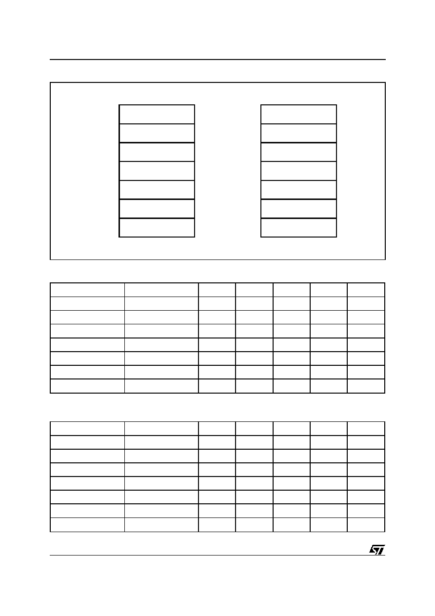
16K BOOT BLOCK
AI01990
3FFFFh
3C000h
3BFFFh
3A000h
39FFFh
00000h
8K PARAMETER BLOCK
8K PARAMETER BLOCK
32K MAIN BLOCK
64K MAIN BLOCK
64K MAIN BLOCK
64K MAIN BLOCK
M29F200T
38000h
37FFFh
30000h
2FFFFh
20000h
1FFFFh
10000h
0FFFFh
M29F200B
16K BOOT BLOCK
8K PARAMETER BLOCK
8K PARAMETER BLOCK
32K MAIN BLOCK
64K MAIN BLOCK
64K MAIN BLOCK
64K MAIN BLOCK
3FFFFh
30000h
2FFFFh
20000h
1FFFFh
10000h
0FFFFh
08000h
07FFFh
04000h
03FFFh
00000h
06000h
05FFFh
Figure 3. Memory Map and Block Address Table (x8)
Address Range (x8)
Address Range (x16)
A16
A15
A14
A13
A12
00000h-03FFFh
00000h-01FFFh
0
0
0
0
X
04000h-05FFFh
02000h-02FFFh
0
0
0
1
0
06000h-07FFFh
03000h-03FFFh
0
0
0
1
1
08000h-0FFFFh
04000h-07FFFh
0
0
1
X
X
10000h-1FFFFh
08000h-0FFFFh
0
1
X
X
X
20000h-2FFFFh
10000h-17FFFh
1
0
X
X
X
30000h-3FFFFh
18000h-1FFFFh
1
1
X
X
X
Table 3B. M29F200B Block Address Table
Address Range (x8)
Address Range (x16)
A16
A15
A14
A13
A12
00000h-0FFFFh
00000h-07FFFh
0
0
X
X
X
10000h-1FFFFh
08000h-0FFFFh
0
1
X
X
X
20000h-2FFFFh
10000h-17FFFh
1
0
X
X
X
30000h-37FFFh
18000h-1BFFFh
1
1
0
X
X
38000h-39FFFh
1C000h-1CFFFh
1
1
1
0
0
3A000h-3BFFFh
1D000h-1DFFFh
1
1
1
0
1
3C000h-3FFFFh
1E000h-1FFFFh
1
1
1
1
X
Table 3A. M29F200T Block Address Table
4/33
M29F200T, M29F200B

Command Interface
Instructions, made up of commands written in cy-
cles, can be given to the Program/Erase Controller
through a Command Interface (C.I.). For added
data protection, program or erase execution starts
after 4 or 6 cycles. The first, second, fourth and fifth
cycles are used to input Coded cycles to the C.I.
This Coded sequence is the same for all Pro-
gram/Erase Controller instructions. The 'Com-
mand' itself and its confirmation, when applicable,
are given on the third, fourth or sixth cycles. Any
incorrect command or any improper command se-
quence will reset the device to Read Array mode.
Instructions
Seven instructions are defined to perform Read
Array, Auto Select (to read the ElectronicSignature
or Block Protection Status), Program, Block Erase,
Chip Erase, Erase Suspend and Erase Resume.
The internal P/E.C. automatically handles all tim-
ing and verification of the Program and Erase
operations. The Status Register Data Polling, Tog-
gle, Error bits and the RB output may be read at
any time, during programming or erase, to monitor
the progress of the operation.
Instructions are composed of up to six cycles. The
first two cycles input a Coded sequence to the
Command Interfacewhich is common to all instruc-
tions (see Table 8). The third cycle inputs the
instruction set-up command. Subsequent cycles
output the addressed data, Electronic Signature or
Block Protection Status for Read operations. In
order to give additional data protection, the instruc-
tions for Program and Block or Chip Erase require
further command inputs. For a Program instruction,
the fourth command cycle inputs the address and
data to be programmed. For an Erase instruction
(Block or Chip), the fourth and fifth cycles input a
further Coded sequence before the Erase confirm
command on the sixth cycle. Erasure of a memory
block may be suspended,in orderto read data from
another block or to program data in another block,
and then resumed.
When power is first applied or if V
CC
falls below
V
LKO
, the command interface is reset to Read
Array.
SIGNAL DESCRIPTIONS
See Figure 1 and Table 1.
Address Inputs (A0-A16). The address inputs for
the memory array are latched during a write opera-
tion on the falling edge of Chip Enable E or Write
Enable W. In Word-wide organisation the address
lines are A0-A16, in Byte-wide organisation
DQ15A≠1 acts as an additional LSB address line.
When A9 is raised to V
ID
, either a Read Electronic
Signature Manufacturer or Device Code, Block
Protection Status or a Write Block Protection or
Block Unprotection is enabled depending on the
combination of levels on A0, A1, A6, A12 and A15.
Data Input/Outputs (DQ0-DQ7). T h e s e I n-
puts/Outputsare used in the Byte-wide and Word-
wide organisations. The input is data to be
programmed in the memory array or a command
to be written to the C.I. Both are latched on the
rising edge of Chip Enable E or Write Enable W.
The output is data from the Memory Array, the
Electronic Signature Manufacturer or Device
codes, the Block Protection Status or the Status
register Data Polling bit DQ7, the Toggle Bits DQ6
and DQ2, the Error bit DQ5 or the Erase Timer bit
DQ3. Outputs are valid when Chip Enable E and
Output Enable G are active. The output is high
impedance when the chip is deselected or the
outputsare disabled and when RP is at a Low level.
Data Input/Outputs (DQ8-DQ14 and DQ15A≠1).
These Inputs/Outputs are additionally used in the
Word-wide organisation. When BYTEis High DQ8-
DQ14 and DQ15A≠1 act as the MSB of the Data
Input or Output, functioning as described for DQ0-
DQ7 above, and DQ8-DQ15 are 'don't care' for
command inputs or status outputs. When BYTE is
Low, DQ8-DQ14 are high impedance, DQ15A≠1 is
the Address A≠1 input.
Chip Enable (E). The Chip Enable input activates
the memory control logic, input buffers, decoders
and sense amplifiers. E High deselectsthe memory
and reduces the power consumption to the standby
level. E can also be used to control writing to the
command register and to the memory array, while
W remains at a low level. The Chip Enable must be
forced to V
ID
during the Block Unprotection opera-
tion.
Output Enable (G). The Output Enable gates the
outputs through the data buffers during a read
operation. When G is High the outputs are High
impedance. G must be forced to V
ID
level during
Block Protection and Unprotection operations.
Write Enable (W). This input controls writing to the
Command Registerand Addressand Data latches.
Byte/Word Organization Select (BYTE) . The
BYTE input selects the output configuration for the
device: Byte-wide (x8) mode or Word-wide (x16)
mode. When BYTE is Low, the Byte-wide mode is
selected and the data is read and programmed on
DQ0-DQ7. In this mode, DQ8-DQ14 are at high
impedance and DQ15A≠1 is the LSB address.
When BYTE is High, the Word-wide mode is se-
lected and the data is read and programmed on
DQ0-DQ15.
5/33
M29F200T, M29F200B