1/22
PRELIMINARY DATA
March 2000
This is preliminary information on a new product now in development or undergoing evaluation. Details are subject to change without notice.
M29F160BT
M29F160BB
16 Mbit (2Mb x8 or 1Mb x16, Boot Block)
Single Supply Flash Memory
s
SINGLE 5V±10% SUPPLY VOLTAGE for
PROGRAM, ERASE and READ OPERATIONS
s
ACCESS TIME: 55ns
s
PROGRAMMING TIME
≠ 8µs per Byte/Word typical
s
35 MEMORY BLOCKS
≠ 1 Boot Block (Top or Bottom Location)
≠ 2 Parameter and 32 Main Blocks
s
PROGRAM/ERASE CONTROLLER
≠ Embedded Byte/Word Program algorithm
≠ Embedded Multi-Block/Chip Erase algorithm
≠ Status Register Polling and Toggle Bits
≠ Ready/Busy Output Pin
s
ERASE SUSPEND and RESUME MODES
≠ Read and Program another Block during
Erase Suspend
s
UNLOCK BYPASS PROGRAM COMMAND
≠ Faster Production/Batch Programming
s
TEMPORARY BLOCK UNPROTECTION
MODE
s
LOW POWER CONSUMPTION
≠ Standby and Automatic Standby
s
100,000 PROGRAM/ERASE CYCLES per
BLOCK
s
20 YEARS DATA RETENTION
≠ Defectivity below 1 ppm/year
s
ELECTRONIC SIGNATURE
≠ Manufacturer Code: 0020h
≠ Top Device Code M29F160BT: 22CCh
≠ Bottom Device Code M29F160BB: 224Bh
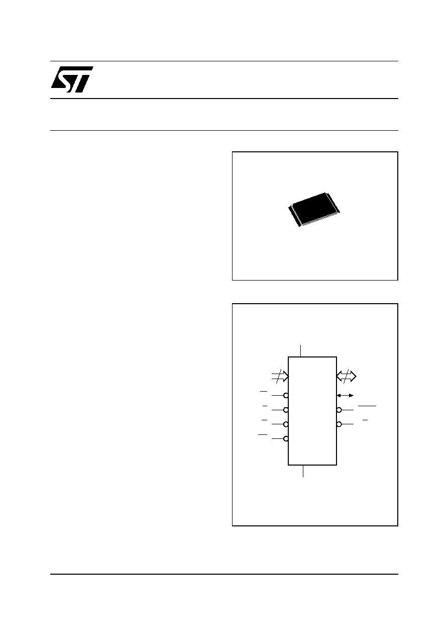
TSOP48 (N)
12 x 20mm
Figure 1. Logic Diagram
AI02920
20
A0-A19
W
DQ0-DQ14
VCC
M29F160BT
M29F160BB
E
VSS
15
G
RP
DQ15A≠1
BYTE
RB
M29F160BT, M29F160BB
2/22
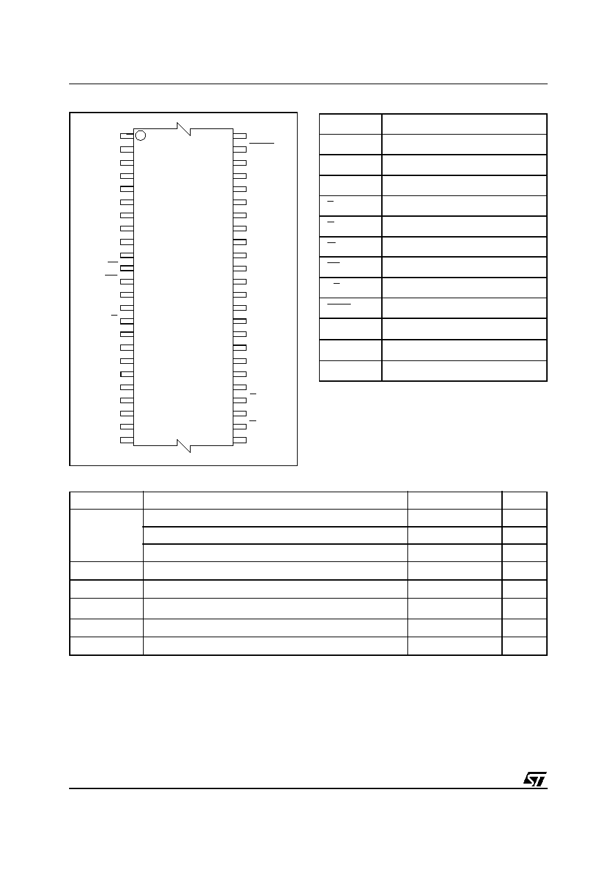
Figure 2. TSOP Connections
DQ3
DQ9
DQ2
A6
DQ0
W
A3
RB
DQ6
A8
A9
DQ13
A17
A10
DQ14
A2
DQ12
DQ10
DQ15A≠1
VCC
DQ4
DQ5
A7
DQ7
NC
NC
AI02921
M29F160BT
M29F160BB
12
1
13
24
25
36
37
48
DQ8
NC
A19
A1
A18
A4
A5
DQ1
DQ11
G
A12
A13
A16
A11
BYTE
A15
A14
VSS
E
A0
RP
VSS
Table 1. Signal Names
A0-A19
Address Inputs
DQ0-DQ7
Data Inputs/Outputs
DQ8-DQ14
Data Inputs/Outputs
DQ15A≠1
Data Input/Output or Address Input
E
Chip Enable
G
Output Enable
W
Write Enable
RP
Reset/Block Temporary Unprotect
RB
Ready/Busy Output
BYTE
Byte/Word Organization Select
V
CC
Supply Voltage
V
SS
Ground
NC
Not Connected Internally
Table 2. Absolute Maximum Ratings
(1)
Note: 1. Except for the rating "Operating Temperature Range", stresses above those listed in the Table "Absolute Maximum Ratings" may
cause permanent damage to the device. These are stress ratings only and operation of the device at these or any other conditions
above those indicated in the Operating sections of this specification is not implied. Exposure to Absolute Maximum Rating condi-
tions for extended periods may affect device reliability. Refer also to the STMicroelectronics SURE Program and other relevant qual-
ity documents.
2. Minimum Voltage may undershoot to ≠2V during transition and for less than 20ns during transitions.
Symbol
Parameter
Value
Unit
T
A
Ambient Operating Temperature (Temperature Range Option 1)
0 to 70
∞C
Ambient Operating Temperature (Temperature Range Option 6)
≠40 to 85
∞C
Ambient Operating Temperature (Temperature Range Option 3)
≠40 to 125
∞C
T
BIAS
Temperature Under Bias
≠50 to 125
∞C
T
STG
Storage Temperature
≠65 to 150
∞C
V
IO
(2)
Input or Output Voltage
≠0.6 to 6
V
V
CC
Supply Voltage
≠0.6 to 6
V
V
ID
Identification Voltage
≠0.6 to 13.5
V

5/22
M29F160BT, M29F160BB
SIGNAL DESCRIPTIONS
See Figure 1, Logic Diagram, and Table 1, Signal
Names, for a brief overview of the signals connect-
ed to this device.
Address Inputs (A0-A19). The Address Inputs
select the cells in the memory array to access dur-
ing Bus Read operations. During Bus Write opera-
tions they control the commands sent to the
Command Interface of the internal state machine.
Data Inputs/Outputs (DQ0-DQ7). The Data In-
puts/Outputs output the data stored at the selected
address during a Bus Read operation. During Bus
Write operations they represent the commands
sent to the Command Interface of the internal state
machine.
Data Inputs/Outputs (DQ8-DQ14). The Data In-
puts/Outputs output the data stored at the selected
address during a Bus Read operation when BYTE
is High, V
IH
. When BYTE is Low, V
IL
, these pins
are not used and are high impedance. During Bus
Write operations the Command Register does not
use these bits. When reading the Status Register
these bits should be ignored.
Data Input/Output or Address Input (DQ15A-1).
When BYTE is High, V
IH
, this pin behaves as a
Data Input/Output pin (as DQ8-DQ14). When
BYTE is Low, V
IL
, this pin behaves as an address
pin; DQ15A≠1 Low will select the LSB of the Word
on the other addresses, DQ15A≠1 High will select
the MSB. Throughout the text consider references
to the Data Input/Output to include this pin when
BYTE is High and references to the Address In-
puts to include this pin when BYTE is Low except
when stated explicitly otherwise.
Chip Enable (E). The Chip Enable, E, activates
the memory, allowing Bus Read and Bus Write op-
erations to be performed. When Chip Enable is
High, V
IH
, all other pins are ignored.
Output Enable (G). The Output Enable, G, con-
trols the Bus Read operation of the memory.
Write Enable (W). The Write Enable, W, controls
the Bus Write operation of the memory's Com-
mand Interface.
Reset/Block Temporary Unprotect (RP). The Re-
set/Block Temporary Unprotect pin can be used to
apply a Hardware Reset to the memory or to tem-
porarily unprotect all blocks that have been pro-
tected.
A Hardware Reset is achieved by holding Reset/
Block Temporary Unprotect Low, V
IL
, for at least
t
PLPX
. After Reset/Block Temporary Unprotect
goes High, V
IH
, the memory will be ready for Bus
Read and Bus Write operations after t
PHEL
or
t
RHEL
, whichever occurs last. See the Ready/Busy
Output section, Table 17 and Figure 10, Reset/
Temporary Unprotect AC Characteristics for more
details.
Holding RP at V
ID
will temporarily unprotect the
protected blocks in the memory. Program and
Erase operations on all blocks will be possible.
The transition from V
IH
to V
ID
must be slower than
t
PHPHH
.
Ready/Busy Output (RB). The Ready/Busy pin
is an open-drain output that can be used to identify
when the memory array can be read. Ready/Busy
is high-impedance during Read mode, Auto Select
mode and Erase Suspend mode.
After a Hardware Reset, Bus Read and Bus Write
operations cannot begin until Ready/Busy be-
comes high-impedance. See Table 17 and Figure
10, Reset/Temporary Unprotect AC Characteris-
tics.
During Program or Erase operations Ready/Busy
is Low, V
OL
. Ready/Busy will remain Low during
Read/Reset commands or Hardware Resets until
the memory is ready to enter Read mode.
The use of an open-drain output allows the Ready/
Busy pins from several memories to be connected
to a single pull-up resistor. A Low will then indicate
that one, or more, of the memories is busy.
Byte/Word Organization Select (BYTE). The Byte/
Word Organization Select pin is used to switch be-
tween the 8-bit and 16-bit Bus modes of the mem-
ory. When Byte/Word Organization Select is Low,
V
IL
, the memory is in 8-bit mode, when it is High,
V
IH
, the memory is in 16-bit mode.
V
CC
Supply Voltage. The V
CC
Supply Voltage
supplies the power for all operations (Read, Pro-
gram, Erase etc.).
The Command Interface is disabled when the V
CC
Supply Voltage is less than the Lockout Voltage,
V
LKO
. This prevents Bus Write operations from ac-
cidentally damaging the data during power up,
power down and power surges. If the Program/
Erase Controller is programming or erasing during
this time then the operation aborts and the memo-
ry contents being altered will be invalid.
A 0.1µF capacitor should be connected between
the V
CC
Supply Voltage pin and the V
SS
Ground
pin to decouple the current surges from the power
supply. The PCB track widths must be sufficient to
carry the currents required during program and
erase operations, I
CC4
.
Vss Ground. The V
SS
Ground is the reference
for all voltage measurements.