 | –≠–ª–µ–∫—Ç—Ä–æ–Ω–Ω—ã–π –∫–æ–º–ø–æ–Ω–µ–Ω—Ç: M29W010 | –°–∫–∞—á–∞—Ç—å:  PDF PDF  ZIP ZIP |
1/19
PRELIMINARY DATA
March 2000
This is preliminary information on a new product now in development or undergoing evaluation. Details are subject to change without notice.
M29W010B
1 Mbit (128Kb x8, Uniform Block)
Low Voltage Single Supply Flash Memory
s
SINGLE 2.7 to 3.6V SUPPLY VOLTAGE for
PROGRAM, ERASE and READ OPERATIONS
s
ACCESS TIME: 45ns
s
PROGRAMMING TIME
≠ 10µs by Byte typical
s
8 UNIFORM 16 Kbyte MEMORY BLOCKS
s
PROGRAM/ERASE CONTROLLER
≠ Embedded Byte Program algorithm
≠ Embedded Multi-Block/Chip Erase algorithm
≠ Status Register Polling and Toggle Bits
s
ERASE SUSPEND and RESUME MODES
≠ Read and Program another Block during
Erase Suspend
s
UNLOCK BYPASS PROGRAM COMMAND
≠ Faster Production/Batch Programming
s
LOW POWER CONSUMPTION
≠ Standby and Automatic Standby
s
100,000 PROGRAM/ERASE CYCLES per
BLOCK
s
20 YEARS DATA RETENTION
≠ Defectivity below 1 ppm/year
s
ELECTRONIC SIGNATURE
≠ Manufacturer Code: 20h
≠ Device Code: 23h
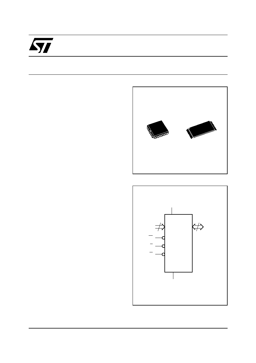
TSOP32 (N)
8 x 20mm
PLCC32 (K)
Figure 1. Logic Diagram
AI02747
17
A0-A16
W
DQ0-DQ7
VCC
M29W010B
E
VSS
8
G
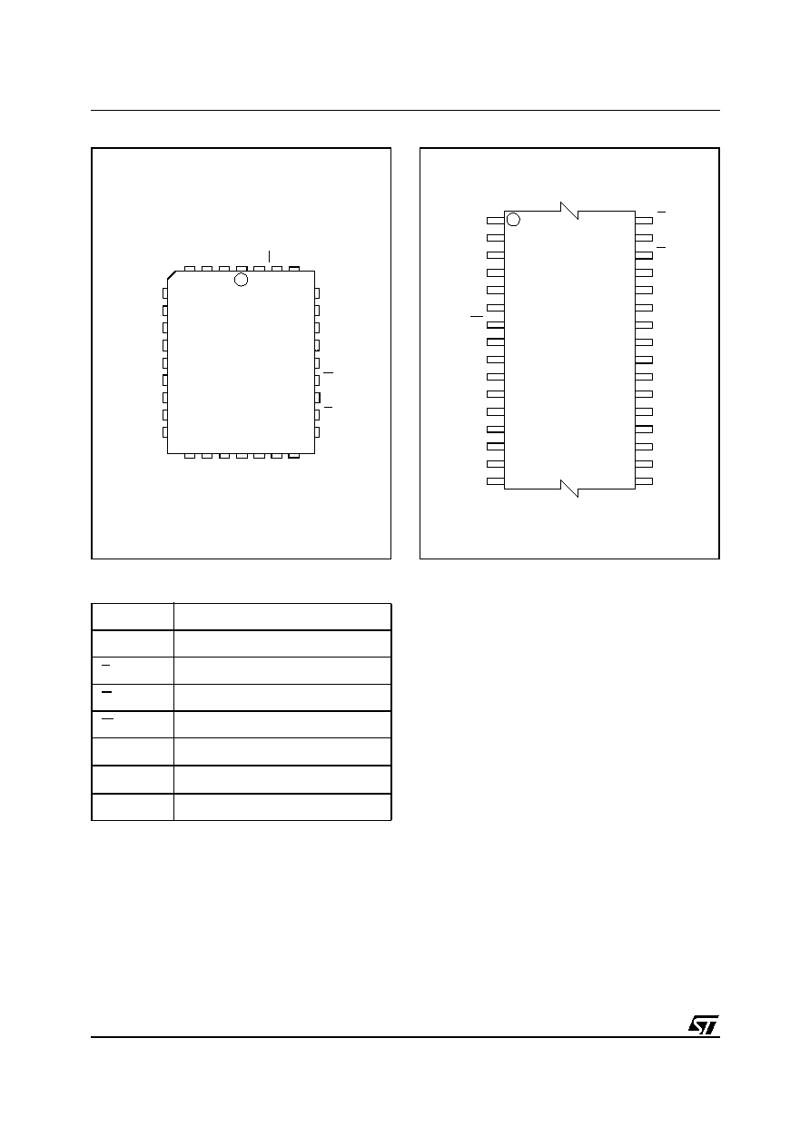
M29W010B
2/19
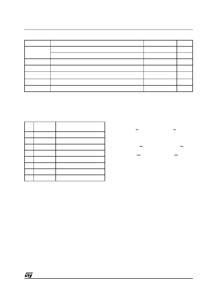
Figure 2. PLCC Connections
AI02748
NC
A13
A10
DQ5
17
A1
A0
DQ0
DQ1
DQ2
DQ3
DQ4
A7
A4
A3
A2
A6
A5
9
W
A8
1
A16
A9
DQ7
A12
A14
32
NC
V
CC
M29W010B
A15
A11
DQ6
G
E
25
V
SS
Table 1. Signal Names
A0-A16
Address Inputs
DQ0-DQ7
Data Inputs/Outputs
E
Chip Enable
G
Output Enable
W
Write Enable
V
CC
Supply Voltage
V
SS
Ground
NC
Not Connected Internally
SUMMARY DESCRIPTION
The M29W010B is a 1 Mbit (128Kb x8) non-vola-
tile memory that can be read, erased and repro-
grammed. These operations can be performed
using a single low voltage (2.7 to 3.6V) supply. On
power-up the memory defaults to its Read mode
where it can be read in the same way as a ROM or
EPROM.
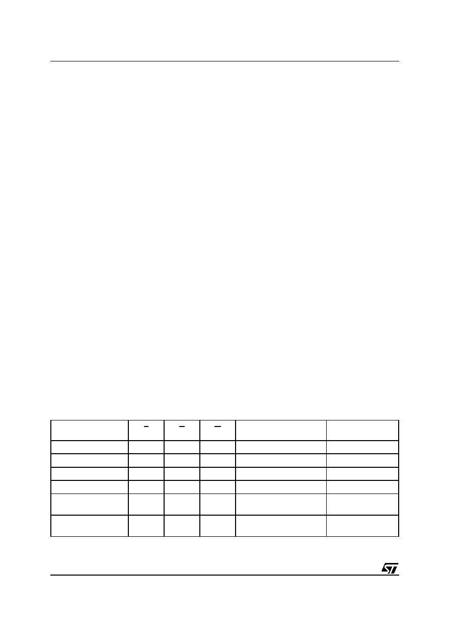
Figure 3. TSOP Connections
A1
A0
DQ0
A7
A4
A3
A2
A6
A5
A13
A10
A8
A9
DQ7
A14
A11
G
E
DQ5
DQ1
DQ2
DQ3
DQ4
DQ6
NC
W
A16
A12
NC
VCC
A15
AI02754
M29W010B
8
1
9
16
17
24
25
32
VSS
The memory is divided into blocks that can be
erased independently so it is possible to preserve
valid data while old data is erased. Each block can
be protected independently to prevent accidental
Program or Erase commands from modifying the
memory. Program and Erase commands are writ-
ten to the Command Interface of the memory. An
on-chip Program/Erase Controller simplifies the
process of programming or erasing the memory by
taking care of all of the special operations that are
required to update the memory contents. The end
of a program or erase operation can be detected
and any error conditions identified. The command
set required to control the memory is consistent
with JEDEC standards.
Chip Enable, Output Enable and Write Enable sig-
nals control the bus operation of the memory.
They allow simple connection to most micropro-
cessors, often without additional logic.
The memory is offered in PLCC32 or TSOP32 (8 x
20mm) packages and it is supplied with all the bits
erased (set to '1').
3/19
M29W010B
SIGNAL DESCRIPTIONS
See Figure 1, Logic Diagram, and Table 1, Signal
Names, for a brief overview of the signals connect-
ed to this device.
Address Inputs (A0-A16). The Address Inputs
select the cells in the memory array to access dur-
ing Bus Read operations. During Bus Write opera-
tions they control the commands sent to the
Command Interface of the internal state machine.
Data Inputs/Outputs (DQ0-DQ7). The Data In-
puts/Outputs output the data stored at the selected
address during a Bus Read operation. During Bus
Write operations they represent the commands
sent to the Command Interface of the internal state
machine.
Chip Enable (E). The Chip Enable, E, activates
the memory, allowing Bus Read and Bus Write op-
erations to be performed. When Chip Enable is
High, V
IH
, all other pins are ignored.
Output Enable (G). The Output Enable, G, con-
trols the Bus Read operation of the memory.
Write Enable (W). The Write Enable, W, controls
the Bus Write operation of the memory's Com-
mand Interface.
V
CC
Supply Voltage. The V
CC
Supply Voltage
supplies the power for all operations (Read, Pro-
gram, Erase etc.).
The Command Interface is disabled when the V
CC
Supply Voltage is less than the Lockout Voltage,
V
LKO
. This prevents Bus Write operations from ac-
cidentally damaging the data during power-up,
power-down and power surges. If the Program/
Erase Controller is programming or erasing during
this time then the operation aborts and the memo-
ry contents being altered will be invalid.
A 0.1µF capacitor should be connected between
the V
CC
Supply Voltage pin and the V
SS
Ground
pin to decouple the current surges from the power
supply. The PCB track widths must be sufficient to
carry the currents required during program and
erase operations, I
CC3
.
V
SS
Ground. The V
SS
Ground is the reference for
all voltage measurements.
Table 2. Absolute Maximum Ratings
(1)
Note: 1. Except for the rating "Operating Temperature Range", stresses above those listed in the Table "Absolute Maximum Ratings" may
cause permanent damage to the device. These are stress ratings only and operation of the device at these or any other conditions
above those indicated in the Operating sections of this specification is not implied. Exposure to Absolute Maximum Rating condi-
tions for extended periods may affect device reliability. Refer also to the STMicroelectronics SURE Program and other relevant qual-
ity documents.
2. Minimum Voltage may undershoot to ≠2V during transition and for less than 20ns during transitions.
Symbol
Parameter
Value
Unit
T
A
Ambient Operating Temperature (Temperature Range Option 1)
0 to 70
∞C
Ambient Operating Temperature (Temperature Range Option 6)
≠40 to 85
∞C
T
BIAS
Temperature Under Bias
≠50 to 125
∞C
T
STG
Storage Temperature
≠65 to 150
∞C
V
IO
(2)
Input or Output Voltage
≠0.6 to 4
V
V
CC
Supply Voltage
≠0.6 to 4
V
V
ID
Identification Voltage
≠0.6 to 13.5
V
Table 3. Uniform Block Addresses, M29W010B
#
Size
(Kbytes)
Address Range
7
16
1C000h-1FFFFh
6
16
18000h-1BFFFh
5
16
14000h-17FFFh
4
16
10000h-13FFFh
3
16
0C000h-0FFFFh
2
16
08000h-0BFFFh
1
16
04000h-07FFFh
0
16
00000h-03FFFh
M29W010B
4/19
BUS OPERATIONS
There are five standard bus operations that control
the device. These are Bus Read, Bus Write, Out-
put Disable, Standby and Automatic Standby. See
Table 4, Bus Operations, for a summary. Typically
glitches of less than 5ns on Chip Enable or Write
Enable are ignored by the memory and do not af-
fect bus operations.
Bus Read. Bus Read operations read from the
memory cells, or specific registers in the Com-
mand Interface. A valid Bus Read operation in-
volves setting the desired address on the Address
Inputs, applying a Low signal, V
IL
, to Chip Enable
and Output Enable and keeping Write Enable
High, V
IH
. The Data Inputs/Outputs will output the
value, see Figure 8, Read Mode AC Waveforms,
and Table 11, Read AC Characteristics, for details
of when the output becomes valid.
Bus Write. Bus Write operations write to the
Command Interface. A valid Bus Write operation
begins by setting the desired address on the Ad-
dress Inputs. The Address Inputs are latched by
the Command Interface on the falling edge of Chip
Enable or Write Enable, whichever occurs last.
The Data Inputs/Outputs are latched by the Com-
mand Interface on the rising edge of Chip Enable
or Write Enable, whichever occurs first. Output En-
able must remain High, V
IH
, during the whole Bus
Write operation. See Figures 9 and 10, Write AC
Waveforms, and Tables 12 and 13, Write AC
Characteristics, for details of the timing require-
ments.
Output Disable. The Data Inputs/Outputs are in
the high impedance state when Output Enable is
High, V
IH
.
Standby. When Chip Enable is High, V
IH
, the
memory enters Standby mode and the Data In-
puts/Outputs pins are placed in the high-imped-
ance state. To reduce the Supply Current to the
Standby Supply Current, I
CC2
, Chip Enable should
be held within V
CC
± 0.2V. For the Standby current
level see Table 10, DC Characteristics.
During program or erase operations the memory
will continue to use the Program/Erase Supply
Current, I
CC3
, for Program or Erase operations un-
til the operation completes.
Automatic Standby. If CMOS levels (V
CC
± 0.2V)
are used to drive the bus and the bus is inactive for
150ns or more the memory enters Automatic
Standby where the internal Supply Current is re-
duced to the Standby Supply Current, I
CC2
. The
Data Inputs/Outputs will still output data if a Bus
Read operation is in progress.
Special Bus Operations
Additional bus operations can be performed to
read the Electronic Signature and also to apply
and remove Block Protection. These bus opera-
tions are intended for use by programming equip-
ment and are not usually used in applications.
They require V
ID
to be applied to some pins.
Electronic Signature. The memory has two
codes, the manufacturer code and the device
code, that can be read to identify the memory.
These codes can be read by applying the signals
listed in Table 4, Bus Operations.
Block Protection and Blocks Unprotection. Each
block can be separately protected against acci-
dental Program or Erase. Protected blocks can be
unprotected to allow data to be changed. Block
Protection and Blocks Unprotection operations
must only be performed on programming equip-
ment. For further information refer to Application
Note AN1122, Applying Protection and Unprotec-
tion to M29 Series Flash.
Table 4. Bus Operations
Note: X = V
IL
or V
IH
.
Operation
E
G
W
Address Inputs
Data
Inputs/Outputs
Bus Read
V
IL
V
IL
V
IH
Cell Address
Data Output
Bus Write
V
IL
V
IH
V
IL
Command Address
Data Input
Output Disable
X
V
IH
V
IH
X
Hi-Z
Standby
V
IH
X
X
X
Hi-Z
Read Manufacturer
Code
V
IL
V
IL
V
IH
A0 = V
IL
, A1 = V
IL
, A9 = V
ID
,
Others V
IL
or V
IH
20h
Read Device Code
V
IL
V
IL
V
IH
A0 = V
IH
, A1 = V
IL
, A9 = V
ID
,
Others V
IL
or V
IH
23h

5/19
M29W010B
COMMAND INTERFACE
All Bus Write operations to the memory are inter-
preted by the Command Interface. Commands
consist of one or more sequential Bus Write oper-
ations. Failure to observe a valid sequence of Bus
Write operations will result in the memory return-
ing to Read mode. The long command sequences
are imposed to maximize data security.
The commands are summarized in Table 5, Com-
mands. Refer to Table 5 in conjunction with the
text descriptions below.
Read/Reset Command. The Read/Reset com-
mand returns the memory to its Read mode where
it behaves like a ROM or EPROM. It also resets
the errors in the Status Register. Either one or
three Bus Write operations can be used to issue
the Read/Reset command.
If the Read/Reset command is issued during a
Block Erase operation or following a Programming
or Erase error then the memory will take upto 10
µs
to abort. During the abort period no valid data can
be read from the memory. Issuing a Read/Reset
command during a Block Erase operation will
leave invalid data in the memory.
Auto Select Command. The Auto Select com-
mand is used to read the Manufacturer Code, the
Device Code and the Block Protection Status.
Three consecutive Bus Write operations are re-
quired to issue the Auto Select command. Once
the Auto Select command is issued the memory
remains in Auto Select mode until another com-
mand is issued.
From the Auto Select mode the Manufacturer
Code can be read using a Bus Read operation
with A0 = V
IL
and A1 = V
IL
. The other address bits
may be set to either V
IL
or V
IH
. The Manufacturer
Code for STMicroelectronics is 20h.
The Device Code can be read using a Bus Read
operation with A0 = V
IH
and A1 = V
IL
. The other
address bits may be set to either V
IL
or V
IH
. The
Device Code for the M29W010B is 23h.
The Block Protection Status of each block can be
read using a Bus Read operation with A0 = V
IL
,
A1 = V
IH
, and A14-A16 specifying the address of
the block. The other address bits may be set to ei-
ther V
IL
or V
IH
. If the addressed block is protected
then 01h is output on the Data Inputs/Outputs, oth-
erwise 00h is output.
Program Command. The Program command
can be used to program a value to one address in
the memory array at a time. The command re-
quires four Bus Write operations, the final write op-
eration latches the address and data in the internal
state machine and starts the Program/Erase Con-
troller.
If the address falls in a protected block then the
Program command is ignored, the data remains
unchanged. The Status Register is never read and
no error condition is given.
During the program operation the memory will ig-
nore all commands. It is not possible to issue any
command to abort or pause the operation. Typical
program times are given in Table 6. Bus Read op-
erations during the program operation will output
the Status Register on the Data Inputs/Outputs.
See the section on the Status Register for more
details.
After the program operation has completed the
memory will return to the Read mode, unless an
error has occurred. When an error occurs the
memory will continue to output the Status Regis-
ter. A Read/Reset command must be issued to re-
set the error condition and return to Read mode.
Note that the Program command cannot change a
bit set at '0' back to '1'. One of the Erase Com-
mands must be used to set all the bits in a block or
in the whole memory from '0' to '1'.
Unlock Bypass Command. The Unlock Bypass
command is used in conjunction with the Unlock
Bypass Program command to program the memo-
ry. When the access time to the device is long (as
with some EPROM programmers) considerable
time saving can be made by using these com-
mands. Three Bus Write operations are required
to issue the Unlock Bypass command.
Once the Unlock Bypass command has been is-
sued the memory will only accept the Unlock By-
pass Program command and the Unlock Bypass
Reset command. The memory can be read as if in
Read mode.
Unlock Bypass Program Command. The Un-
lock Bypass Program command can be used to
program one address in memory at a time. The
command requires two Bus Write operations, the
final write operation latches the address and data
in the internal state machine and starts the Pro-
gram/Erase Controller.
The Program operation using the Unlock Bypass
Program command behaves identically to the Pro-
gram operation using the Program command. A
protected block cannot be programmed; the oper-
ation cannot be aborted and the Status Register is
read. Errors must be reset using the Read/Reset
command, which leaves the device in Unlock By-
pass Mode. See the Program command for details
on the behavior.
Unlock Bypass Reset Command. The Unlock
Bypass Reset command can be used to return to
Read/Reset mode from Unlock Bypass Mode.
Two Bus Write operations are required to issue the
Unlock Bypass Reset command.