
AI02074
19
A0-A18
W
DQ0-DQ7
VCC
M29W040
G
E
VSS
8
Figure 1. Logic Diagram
M29W040
4 Mbit (512Kb x8, Uniform Block)
Low Voltage Single Supply Flash Memory
NOT FOR NEW DESIGN
M29W040 is replaced by the M29W040B
2.7V to 3.6V SUPPLY VOLTAGE for
PROGRAM, ERASE and READ OPERATIONS
FAST ACCESS TIME: 100ns
BYTE PROGRAMMING TIME: 12
µ
s typical
ERASE TIME
≠ Block: 1.5 sec typical
≠ Chip: 2.5 sec typical
PROGRAM/ERASE CONTROLLER (P/E.C.)
≠ Program Byte-by-Byte
≠ Data Polling and Toggle bits Protocol for
P/E.C. Status
MEMORY ERASE in BLOCKS
≠ 8 Uniform Blocks of 64 KBytes each
≠ Block Protection
≠ Multiblock Erase
ERASE SUSPEND and RESUME MODES
LOW POWER CONSUMPTION
≠ Read mode: 8mA typical (at 12MHz)
≠ Stand-by mode: 20
µ
A typical
≠ Automatic Stand-by mode
POWER DOWN SOFTWARE COMMAND
≠ Power-down mode: 1
µ
A typical
100,000 PROGRAM/ERASE CYCLES per
BLOCK
20 YEARS DATA RETENTION
≠ Defectivity below 1ppm/year
ELECTRONIC SIGNATURE
≠ Manufacturer Code: 20h
≠ Device Code: E3h
A0-A18
Address Inputs
DQ0-DQ7
Data Input / Outputs
E
Chip Enable
G
Output Enable
W
Write Enable
V
CC
Supply Voltage
V
SS
Ground
Table 1. Signal Names
PLCC32 (K)
TSOP32 (N)
8 x 20mm
November 1999
1/31
This is information on a product still in productionbut not recommended for new designs.
TSOP32 (NZ)
8 x 14mm

A1
A0
DQ0
A7
A4
A3
A2
A6
A5
A13
A10
A8
A9
DQ7
A14
A11
G
E
DQ5
DQ1
DQ2
DQ3
DQ4
DQ6
A17
W
A16
A12
A18
VCC
A15
AI02076
M29W040
(Normal)
8
1
9
16
17
24
25
32
VSS
Figure 2B. TSOP Pin Connections
AI02075
A17
A13
A10
DQ5
17
A1
A0
DQ0
DQ1
DQ2
DQ3
DQ4
A7
A4
A3
A2
A6
A5
9
W
A8
1
A16
A9
DQ7
A12
A14
32
A18
V
CC
M29W040
A15
A11
DQ6
G
E
25
V
SS
Figure 2A. LCC Pin Connections
A1
A0
DQ0
A7
A4
A3
A2
A6
A5
A13
A10
A8
A9
DQ7
A14
A11
G
E
DQ5
DQ1
DQ2
DQ3
DQ4
DQ6
A17
W
A16
A12
A18
VCC
A15
AI02077
M29W040
(Reverse)
8
1
9
16
17
24
25
32
VSS
Figure 2C. TSOP Reverse Pin Connections
DESCRIPTION
The M29W040 is a non-volatile memory that may
be erased electrically at the block level, and pro-
grammed Byte-by-Byte.
The interface is directly compatible with most mi-
croprocessors. PLCC32, TSOP32 (8 x 20mm) and
TSOP32 (8 x 14mm) packages are available. Both
normal and reverse pin outs are available for the
TSOP32 (8 x 20mm) package.
Organisation
The FlashMemory organisation is 512K x8 bits with
Address lines A0-A18 and Data Inputs/Outputs
DQ0-DQ7. Memory control is provided by Chip
Enable, Output Enable and Write Enable Inputs.
Erase and Program are performed through the
internal Program/Erase Controller (P/E.C.).
Data Outputs bits DQ7 and DQ6 provide polling or
toggle signals during Automatic Program or Erase
to indicate the Ready/Busy state of the internal
Program/Erase Controller.
Memory Blocks
Erasure of the memory is in blocks. There are 8
uniform blocks of 64 Kbytes each in the memory
address space. Each block can be programmed
and erased over 100,000 cycles. Each uniform
2/31
M29W040
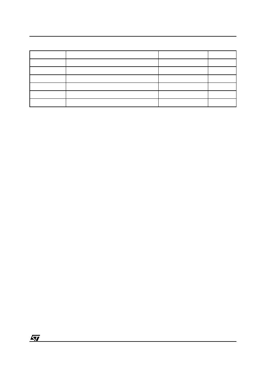
Symbol
Parameter
Value
Unit
T
A
Ambient Operating Temperature
(3)
≠40 to 85
∞
C
T
BIAS
Temperature Under Bias
≠50 to 125
∞
C
T
STG
Storage Temperature
≠65 to 150
∞
C
V
IO
(2)
Input or Output Voltages
≠0.6 to 5
V
V
CC
Supply Voltage
≠0.6 to 5
V
V
A9
(2)
A9 Voltage
≠0.6 to 13.5
V
Notes: 1. Except for the rating "Operating Temperature Range", stresses above those listed in the Table "Absolute Maximum Ratings"
may cause permanent damage to the device. These are stress ratings only and operation of the device at these or any other
conditions above those indicated in the Operating sections of this specification is not implied. Exposure to Absolute Maximum
Rating conditions for extended periods may affect device reliability. Refer also to the STMicroelectronics SURE Program and other
relevant quality documents.
2. Minimum Voltage may undershoot to ≠2V during transition and for less than 20ns.
3. Depends on range.
Table 2. Absolute Maximum Ratings
(1)
block may separately be protected and unpro-
tected against program and erase. Block erasure
may be suspended, while data is read from other
blocks of the memory, and then resumed.
Bus Operations
Seven operations can be performed by the appro-
priate bus cycles, Read Array, Read Electronic
Signature, Output Disable, Standby,Protect Block,
Unprotect Block, and Write the Command of an
Instruction.
Command Interface
Command Bytes can be written to a Command
Interface (C.I.) latch to perform Reading (from the
Array or Electronic Signature), Erasure or Pro-
gramming. For added data protection, command
execution starts after 4 or 6 command cycles. The
first, second, fourth and fifth cycles are used to
input a code sequence to the Command Interface
(C.I.). This sequence is equal for all P/E.C. instruc-
tions. Command itself and its confirmation - if it
applies - are given on the third and fourth or sixth
cycles.
Instructions
Eight instructions are defined to perform Reset,
Read Electronic Signature, Auto Program, Block
Auto Erase, Chip Auto Erase, Block Erase Sus-
pend, Block Erase Resume and Power Down. The
internal Program/EraseController (P/E.C.) handles
all timing and verification of the Program and Erase
instructions and provides Data Polling, Toggle, and
Status data to indicate completion of Program and
Erase Operations.
Instructions are composed of up to six cycles. The
first two cycles input a code sequence to the Com-
mand Interface which is common to all P/E.C.
instructions (see Table 7 for Command Descrip-
tions). The third cycle inputs the instruction set up
command instruction to the Command Interface.
Subsequentcycles output Signature, Block Protec-
tion or the addressed data for Read operations.
For added data protection, the instructions for pro-
gram, and block or chip erase require further com-
mand inputs. For a Program instruction, the fourth
command cycle inputs the address and data to be
programmed. For an Erase instruction (block or
chip), the fourth and fifth cycles input a further code
sequence before the Erase confirm command on
the sixth cycle. Byte programming takes typically
12
µ
s while erase is performed in typically 1.5 sec-
ond.
Erasure of a memory block may be suspended, in
order to read data from another block, and then
resumed. Data Polling, Toggle and Error data may
be read at any time, including during the program-
ming or erase cycles, to monitor the progress of
the operation. When power is first applied or if V
CC
falls below V
LKO
, the command interface is reset to
Read Array.
3/31
M29W040

Operation
E
G
W
DQ0 - DQ7
Read
V
IL
V
IL
V
IH
Data Output
Write
V
IL
V
IH
V
IL
Data Input
Output Disable
V
IL
V
IH
V
IH
Hi-Z
Standby
V
IH
X
X
Hi-Z
Note: X = V
IL
or V
IH
Table 3. Operations
Code
E
G
W
A0
A1
A6
A9
Other
Addresses
DQ0 - DQ7
Manufact. Code
V
IL
V
IL
V
IH
V
IL
V
IL
V
IL
V
ID
Don't Care
20h
Device Code
V
IL
V
IL
V
IH
V
IH
V
IL
V
IL
V
ID
Don't Care
E3h
Table 4. Electronic Signature
Code
E
G
W
A0
A1
A6
A16
A17
A18
Other
Addresses
DQ0 - DQ7
Protected Block
V
IL
V
IL
V
IH
V
IL
V
IH
V
IL
SA
SA
SA
Don't Care
01h
Unprotected Block
V
IL
V
IL
V
IH
V
IL
V
IH
V
IL
SA
SA
SA
Don't Care
00h
Note: SA = Address of block being checked
Table 5. Block Protection Status
DEVICE OPERATION
Signal Descriptions
Address Inputs (A0-A18). The address inputs for
the memory array are latched during a write opera-
tion. The A9 address input is used also for the
Electronic Signature read and Block Protect veri-
fication. When A9 is raised to V
ID
, either a Read
Manufacturer Code, Read Device Code or Verify
Block Protection is enabled depending on the com-
bination of levels on A0, A1 and A6. When A0, A1
and A6 are Low, the ElectronicSignature Manufac-
turer code is read, when A0 is High and A1 and A6
are Low, the Device code is read, and when A1 is
High and A0 and A6 are low, the Block Protection
Status with protect/unprotect algorithm is read for
the block addressed by A16, A17, A18.
Data Input/Outputs (DQ0-DQ7). The data input is
a byte to be programmed or a command written to
the C.I. Both are latched when Chip Enable E and
Write Enable W are active. The data output is from
the memory Array, the Electronic Signature, the
Data Polling bit (DQ7), the Toggle Bit (DQ6), the
Error bit (DQ5) or the Erase Timer bit (DQ3). Ou-
puts are valid when Chip Enable E and Output
Enable G are active. The output is high impedance
when the chip is deselected or the outputs are
disabled.
Chip Enable (E). The Chip Enable activates the
memory control logic, input buffers, decoders and
sense amplifiers. E High deselectsthe memory and
reduces the power consumption to the standby
level. E can also be used to control writing to the
command register and to the memory array, while
W remains at a low level. Addresses are then
latchedon the falling edge of E while data is latched
on the rising edge of E. The Chip Enable must be
forced to V
ID
during Block Unprotect operations.
Output Enable (G). The Output Enable gates the
outputs through the data buffers during a read
operation. G must be forced to V
ID
level during
Block Protect and Block Unprotect operations.
Write Enable (W). This input controls writing to the
Command Register and Address and Data latches.
Addressesare latchedon the falling edge of W, and
Data Inputs are latched on the rising edge of W.
V
CC
Supply Voltage. The power supply for all
operations (Read, Program and Erase).
V
SS
Ground. V
SS
is the reference for all voltage
measurements.
4/31
M29W040
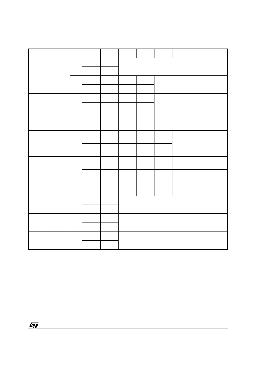
Mne.
Instr.
Cyc.
1st Cyc. 2nd Cyc. 3rd Cyc. 4th Cyc. 5th Cyc. 6th Cyc.
7th Cyc.
RST
(3,9)
Read Array/
Reset
1+
Addr.
(2,6)
X
Read Memory Array until a new write cycle is initiated.
Data
F0h
3+
Addr.
(2,6)
5555h
2AAAh
5555h
Read Memory Array until a new write
cycle is initiated.
Data
AAh
55h
F0h
RSIG
(3)
Read
Electronic
Signature
3+
Addr.
(2,6)
5555h
2AAAh
5555h
Read Electronic Signature until a new
write cycle is initiated. See Note 4.
Data
AAh
55h
90h
RBP
(3)
Read Block
Protection
3+
Addr.
(2,6)
5555h
2AAAh
5555h
Read Block Protection until a new write
cycle is initiated. See Note 5.
Data
AAh
55h
90h
PG
Program
4
Addr.
(2,6)
5555h
2AAAh
5555h
Program
Address Read Data Polling or Toggle Bit
until Program completes.
Data
AAh
55h
A0h
Program
Data
BE
Block Erase
6
Addr.
(2,6)
5555h
2AAAh
5555h
5555h
2AAAh
Block
Address
Additional
Block
(7)
Data
AAh
55h
80h
AAh
55h
30h
30h
CE
Chip Erase
6
Addr.
(2,6)
5555h
2AAAh
5555h
5555h
2AAAh
5555h
Note 8
Data
AAh
55h
80h
AAh
55h
10h
ES
Erase
Suspend
1
Addr.
(2,6)
X
Read until Toggle stops, then read all the data needed from any
uniform block(s) not being erased then Resume Erase.
Data
B0h
ER
Erase
Resume
1
Addr.
(2,6)
X
Read Data Polling or Toggle Bit until Erase completes or Erase
is suspended another time
Data
30h
PD
(10)
Power
Down
1
Addr.
(2,6)
5555h
Puts the memory in Power Down mode where power
consumption is reduced to typically less than 1
µ
A
Data
20h
Notes: 1. Command not interpreted in this table will default to read array mode.
2. X = Don't Care.
3. The first cycle of the RST, RBP or RSIG instruction is followed by read operations to read memory array, Status Register or
Electronic Signature codes. Any number of read cycles can occur after one command cycle.
4. Signature Address bits A0, A1, A6 at V
IL
will output Manufacturer code (20h). Address bits A0 at V
IH
and A1, A6 at V
IL
will output
Device code.
5. Protection Address: A0, A6 at V
IL
, A1 at V
IH
and A16, A17, A18 within the uniform block to be checked, will output the
Block Protection status.
6. Address bits A15-A18 are don't care for coded address inputs.
7. Optional, additional blocks addresses must be entered within a 80
µ
s delay after last write entry, timeout status can be verified
through DQ3 value. When full command is entered, read Data Polling or Toggle bit until Erase is completed or suspended.
8. Read Data Polling or Toggle bit until Erase completes.
9. A wait time of 5
µ
s is necessary after a Reset command, if the memory is in a Block Erase or Power Down status, before
starting any operation.
10. Writing an RST command to the P/E.C. is mandatory prior to any new operation when the memory is in Power Down mode.
Table 6. Instructions
(1)
5/31
M29W040