1/25
PRELIMINARY DATA
February 2000
This is preliminary information on a new product now in development or undergoing evaluation. Details are subject to change without notice.
M29W160BT
M29W160BB
16 Mbit (2Mb x8 or 1Mb x16, Boot Block)
Low Voltage Single Supply Flash Memory
s
SINGLE 2.7 to 3.6V SUPPLY VOLTAGE for
PROGRAM, ERASE and READ OPERATIONS
s
ACCESS TIME: 70ns
s
PROGRAMMING TIME
≠ 10
µ
s per Byte/Word typical
s
35 MEMORY BLOCKS
≠ 1 Boot Block (Top or Bottom Location)
≠ 2 Parameter and 32 Main Blocks
s
PROGRAM/ERASE CONTROLLER
≠ Embedded Byte/Word Program algorithm
≠ Embedded Multi-Block/Chip Erase algorithm
≠ Status Register Polling and Toggle Bits
≠ Ready/Busy Output Pin
s
ERASE SUSPEND and RESUME MODES
≠ Read and Program another Block during
Erase Suspend
s
UNLOCK BYPASS PROGRAM COMMAND
≠ Faster Production/Batch Programming
s
TEMPORARY BLOCK UNPROTECTION
MODE
s
SECURITY MEMORY BLOCK
s
LOW POWER CONSUMPTION
≠ Standby and Automatic Standby
s
100,000 PROGRAM/ERASE CYCLES per
BLOCK
s
20 YEARS DATA RETENTION
≠ Defectivity below 1 ppm/year
s
ELECTRONIC SIGNATURE
≠ Manufacturer Code: 0020h
≠ Top Device Code M29W160BT: 22C4h
≠ Bottom Device Code M29W160BB: 2249h
44
1
TSOP48 (N)
12 x 20mm
SO44 (M)
LFBGA48 (ZA)
8 x 6 solder balls
FBGA
Figure 1. Logic Diagram
Note: RB not available on SO44 package.
AI00981
20
A0-A19
W
DQ0-DQ14
VCC
M29W160BT
M29W160BB
E
VSS
15
G
RP
DQ15A≠1
BYTE
RB
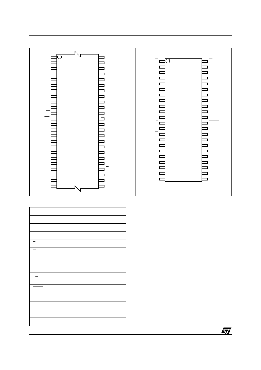
M29W160BT, M29W160BB
2/25
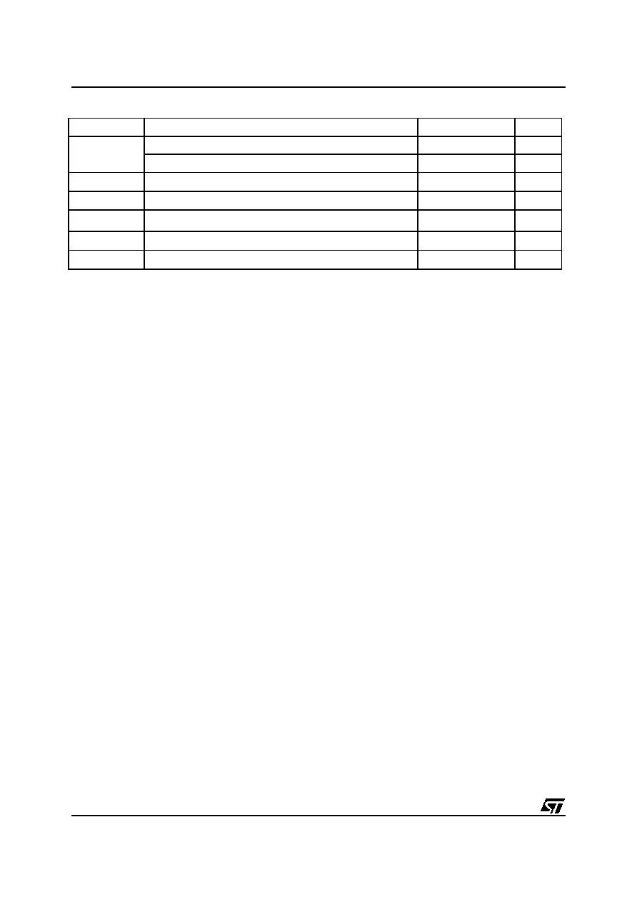
Figure 2. TSOP Connections
DQ3
DQ9
DQ2
A6
DQ0
W
A3
RB
DQ6
A8
A9
DQ13
A17
A10
DQ14
A2
DQ12
DQ10
DQ15A≠1
VCC
DQ4
DQ5
A7
DQ7
NC
NC
AI02994
M29W160BT
M29W160BB
12
1
13
24
25
36
37
48
DQ8
NC
A19
A1
A18
A4
A5
DQ1
DQ11
G
A12
A13
A16
A11
BYTE
A15
A14
VSS
E
A0
RP
VSS
Figure 3. SO Connections
G
DQ0
DQ8
A3
A0
E
VSS
A2
A1
A13
VSS
A14
A15
DQ7
A12
A16
BYTE
DQ15A≠1
DQ5
DQ2
DQ3
VCC
DQ11
DQ4
DQ14
A9
A19
RP
A4
W
A7
AI00978
M29W160BT
M29W160BB
8
2
3
4
5
6
7
9
10
11
12
13
14
15
16
32
31
30
29
28
27
26
25
24
23
22
20
19
18
17
DQ1
DQ9
A6
A5
DQ6
DQ13
44
39
38
37
36
35
34
33
A11
A10
DQ10
21
DQ12
40
43
1
42
41
A17
A8
A18
Table 1. Signal Names
A0-A19
Address Inputs
DQ0-DQ7
Data Inputs/Outputs
DQ8-DQ14
Data Inputs/Outputs
DQ15A≠1
Data Input/Output or Address Input
E
Chip Enable
G
Output Enable
W
Write Enable
RP
Reset/Block Temporary Unprotect
RB
Ready/Busy Output
(Not available on SO44 package)
BYTE
Byte/Word Organization Select
V
CC
Supply Voltage
V
SS
Ground
NC
Not Connected Internally
DU
Don't Use as internally connected
M29W160BT, M29W160BB
4/25
SUMMARY DESCRIPTION
The M29W160B is a 16 Mbit (2Mb x8 or 1Mb x16)
non-volatile memory that can be read, erased and
reprogrammed. These operations can be per-
formed using a single low voltage (2.7 to 3.6V)
supply. On power-up the memory defaults to its
Read mode where it can be read in the same way
as a ROM or EPROM.
The memory is divided into blocks that can be
erased independently so it is possible to preserve
valid data while old data is erased. Each block can
be protected independently to prevent accidental
Program or Erase commands from modifying the
memory. Program and Erase commands are writ-
ten to the Command Interface of the memory. An
on-chip Program/Erase Controller simplifies the
process of programming or erasing the memory by
taking care of all of the special operations that are
required to update the memory contents.
Table 2. Absolute Maximum Ratings
(1)
Note: 1. Except for the rating "Operating Temperature Range", stresses above those listed in the Table "Absolute Maximum Ratings" may
cause permanent damage to the device. These are stress ratings only and operation of the device at these or any other conditions
above those indicated in the Operating sections of this specification is not implied. Exposure to Absolute Maximum Rating condi-
tions for extended periods may affect device reliability. Refer also to the STMicroelectronics SURE Program and other relevant qual-
ity documents.
2. Minimum Voltage may undershoot to ≠2V during transition and for less than 20ns during transitions.
Symbol
Parameter
Value
Unit
T
A
Ambient Operating Temperature (Temperature Range Option 1)
0 to 70
∞
C
Ambient Operating Temperature (Temperature Range Option 6)
≠40 to 85
∞
C
T
BIAS
Temperature Under Bias
≠50 to 125
∞
C
T
STG
Storage Temperature
≠65 to 150
∞
C
V
IO
(2)
Input or Output Voltage
≠0.6 to 4
V
V
CC
Supply Voltage
≠0.6 to 4
V
V
ID
Identification Voltage
≠0.6 to 13.5
V
The end of a program or erase operation can be
detected and any error conditions identified. The
command set required to control the memory is
consistent with JEDEC standards.
The blocks in the memory are asymmetrically ar-
ranged, see Tables 3 and 4, Block Addresses. The
first or last 64 Kbytes have been divided into four
additional blocks. The 16 Kbyte Boot Block can be
used for small initialization code to start the micro-
processor, the two 8 Kbyte Parameter Blocks can
be used for parameter storage and the remaining
32K is a small Main Block where the application
may be stored.
Chip Enable, Output Enable and Write Enable sig-
nals control the bus operation of the memory.
They allow simple connection to most micropro-
cessors, often without additional logic.
The memory is offered in TSOP48 (12 x 20mm),
SO44 and LFBGA48 (0.8mm pitch) packages and
it is supplied with all the bits erased (set to '1').

5/25
M29W160BT, M29W160BB
Table 3. Top Boot Block Addresses,
M29W160BT
#
Size
(Kbytes)
Address Range
(x8)
Address Range
(x16)
34
16
1FC000h-1FFFFFh
FE000h-FFFFF h
33
8
1FA000h-1FBFFFh
FD000h-FDFFFh
32
8
1F8000h-1F9FFFh
FC000h-FCFFFh
31
32
1F0000h-1F7FFFh
F8000h-FBFFFh
30
64
1E0000h-1EFFFFh
F0000h-F7FFFh
29
64
1D0000h-1DFFFFh
E8000h-EFFFFh
28
64
1C0000h-1CFFFFh
E0000h-E7FFFh
27
64
1B0000h-1BFFFFh
D8000h-DFFFFh
26
64
1A0000h-1AFFFFh
D0000h-D7FFFh
25
64
190000h-19FFFFh
C8000h-CFFFFh
24
64
180000h-18FFFFh
C0000h-C7FFFh
23
64
170000h-17FFFFh
B8000h-BFFFFh
22
64
160000h-16FFFFh
B0000h-B7FFFh
21
64
150000h-15FFFFh
A8000h-AFFFFh
20
64
140000h-14FFFFh
A0000h-A7FFFh
19
64
130000h-13FFFFh
98000h-9FFFFh
18
64
120000h-12FFFFh
90000h-97FFFh
17
64
110000h-11FFFFh
88000h-8FFFFh
16
64
100000h-10FFFFh
80000h-87FFFh
15
64
0F0000h-0FFFFFh
78000h-7FFFFh
14
64
0E0000h-0EFFFFh
70000h-77FFFh
13
64
0D0000h-0DFFFFh
68000h-6FFFFh
12
64
0C0000h-0CFFFFh
60000h-67FFFh
11
64
0B0000h-0BFFFFh
58000h-5FFFFh
10
64
0A0000h-0AFFFFh
50000h-57FFFh
9
64
090000h-09FFFFh
48000h-4FFFFh
8
64
080000h-08FFFFh
40000h-47FFFh
7
64
070000h-07FFFFh
38000h-3FFFFh
6
64
060000h-06FFFFh
30000h-37FFFh
5
64
050000h-05FFFFh
28000h-2FFFFh
4
64
040000h-04FFFFh
20000h-27FFFh
3
64
030000h-03FFFFh
18000h-1FFFFh
2
64
020000h-02FFFFh
10000h-17FFFh
1
64
010000h-01FFFFh
08000h-0FFFFh
0
64
000000h-00FFFFh
00000h-07FFFh
Table 4. Bottom Boot Block Addresses,
M29W160BB
#
Size
(Kbytes)
Address Range
(x8)
Address Range
(x16)
34
64
1F0000h-1FFFFFh
F8000h-FFFFFh
33
64
1E0000h-1EFFFFh
F0000h-F7FFFh
32
64
1D0000h-1DFFFFh
E8000h-EFFFFh
31
64
1C0000h-1CFFFFh
E0000h-E7FFFh
30
64
1B0000h-1BFFFFh
D8000h-DFFFF h
29
64
1A0000h-1AFFFFh
D0000h-D7FFFh
28
64
190000h-19FFFFh
C8000h-CFFFF h
27
64
180000h-18FFFFh
C0000h-C7FFFh
26
64
170000h-17FFFFh
B8000h-BFFFFh
25
64
160000h-16FFFFh
B0000h-B7FFFh
24
64
150000h-15FFFFh
A8000h-AFFFFh
23
64
140000h-14FFFFh
A0000h-A7FFFh
22
64
130000h-13FFFFh
98000h-9FFFF h
21
64
120000h-12FFFFh
90000h-97FFFh
20
64
110000h-11FFFFh
88000h-8FFFF h
19
64
100000h-10FFFFh
80000h-87FFFh
18
64
0F0000h-0FFFFFh
78000h-7FFFF h
17
64
0E0000h-0EFFFFh
70000h-77FFFh
16
64
0D0000h-0DFFFFh
68000h-6FFFF h
15
64
0C0000h-0CFFFFh
60000h-67FFFh
14
64
0B0000h-0BFFFFh
58000h-5FFFF h
13
64
0A0000h-0AFFFFh
50000h-57FFFh
12
64
090000h-09FFFFh
48000h-4FFFF h
11
64
080000h-08FFFFh
40000h-47FFFh
10
64
070000h-07FFFFh
38000h-3FFFF h
9
64
060000h-06FFFFh
30000h-37FFFh
8
64
050000h-05FFFFh
28000h-2FFFF h
7
64
040000h-04FFFFh
20000h-27FFFh
6
64
030000h-03FFFFh
18000h-1FFFF h
5
64
020000h-02FFFFh
10000h-17FFFh
4
64
010000h-01FFFFh
08000h-0FFFF h
3
32
008000h-00FFFFh
04000h-07FFFh
2
8
006000h-007FFFh
03000h-03FFFh
1
8
004000h-005FFFh
02000h-02FFFh
0
16
000000h-003FFFh
00000h-01FFFh
