Äîêóìåíòàöèÿ è îïèñàíèÿ www.docs.chipfind.ru
1/36
PRELIMINARY DATA
February 2003
This is preliminary information on a new product now in development or undergoing evaluation. Details are subject to change without notice.
M29W400DT
M29W400DB
4 Mbit (512Kb x8 or 256Kb x16, Boot Block)
3V Supply Flash Memory
FEATURES SUMMARY
s
SUPPLY VOLTAGE
V
CC
=
2.7V to 3.6V for Program, Erase and
Read
s
ACCESS TIME: 45, 55, 70ns
s
PROGRAMMING TIME
10µs per Byte/Word typical
s
11 MEMORY BLOCKS
1 Boot Block (Top or Bottom Location)
2 Parameter and 8 Main Blocks
s
PROGRAM/ERASE CONTROLLER
Embedded Byte/Word Program algorithms
s
ERASE SUSPEND and RESUME MODES
Read and Program another Block during
Erase Suspend
s
UNLOCK BYPASS PROGRAM COMMAND
Faster Production/Batch Programming
s
TEMPORARY BLOCK UNPROTECTION
MODE
s
LOW POWER CONSUMPTION
Standby and Automatic Standby
s
100,000 PROGRAM/ERASE CYCLES per
BLOCK
s
ELECTRONIC SIGNATURE
Manufacturer Code: 0020h
Top Device Code M29W400DT: 00EEh
Bottom Device Code M29W400DB: 00EFh
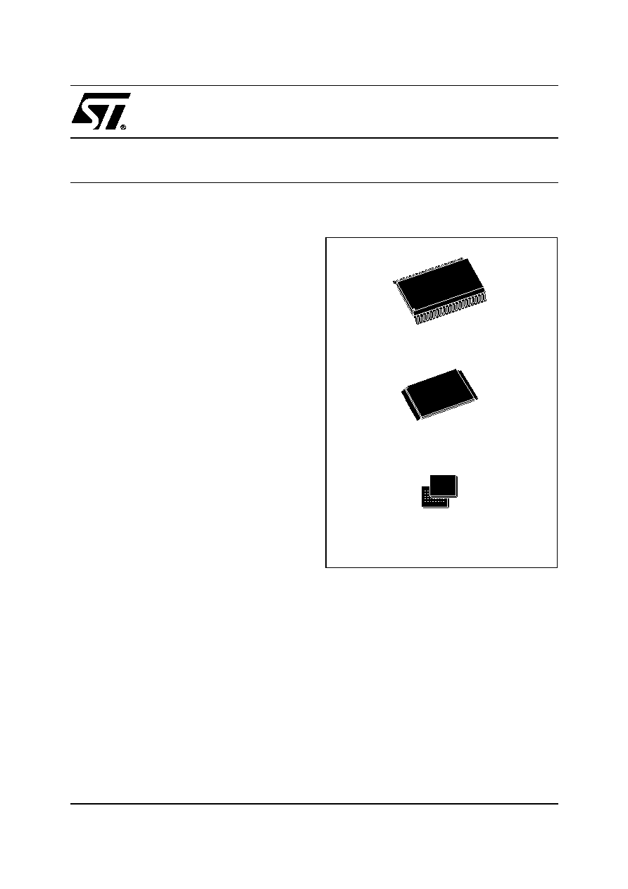
Figure 1. Packages
TSOP48 (N)
12 x 20mm
TFBGA48 (ZA)
6 x 9mm
FBGA
SO44 (M)

M29W400DT, M29W400DB
2/36
TABLE OF CONTENTS
SUMMARY DESCRIPTION . . . . . . . . . . . . . . . . . . . . . . . . . . . . . . . . . . . . . . . . . . . . . . . . . . . . . . . . . . . 5
Figure 2. Logic Diagram . . . . . . . . . . . . . . . . . . . . . . . . . . . . . . . . . . . . . . . . . . . . . . . . . . . . . . . . . . 5
Table 1. Signal Names . . . . . . . . . . . . . . . . . . . . . . . . . . . . . . . . . . . . . . . . . . . . . . . . . . . . . . . . . . . 5
Figure 3. SO Connections . . . . . . . . . . . . . . . . . . . . . . . . . . . . . . . . . . . . . . . . . . . . . . . . . . . . . . . . . 6
Figure 4. TSOP Connections. . . . . . . . . . . . . . . . . . . . . . . . . . . . . . . . . . . . . . . . . . . . . . . . . . . . . . . 6
Figure 5. TFBGA Connections (Top view through package) . . . . . . . . . . . . . . . . . . . . . . . . . . . . . . . 7
Figure 6. Block Addresses (x8) . . . . . . . . . . . . . . . . . . . . . . . . . . . . . . . . . . . . . . . . . . . . . . . . . . . . . 8
Figure 7. Block Addresses (x16) . . . . . . . . . . . . . . . . . . . . . . . . . . . . . . . . . . . . . . . . . . . . . . . . . . . . 9
SIGNAL DESCRIPTIONS . . . . . . . . . . . . . . . . . . . . . . . . . . . . . . . . . . . . . . . . . . . . . . . . . . . . . . . . . . . 10
Address Inputs (A0-A17). . . . . . . . . . . . . . . . . . . . . . . . . . . . . . . . . . . . . . . . . . . . . . . . . . . . . . . . . 10
Data Inputs/Outputs (DQ0-DQ7). . . . . . . . . . . . . . . . . . . . . . . . . . . . . . . . . . . . . . . . . . . . . . . . . . . 10
Data Inputs/Outputs (DQ8-DQ14). . . . . . . . . . . . . . . . . . . . . . . . . . . . . . . . . . . . . . . . . . . . . . . . . . 10
Data Input/Output or Address Input (DQ15A-1). . . . . . . . . . . . . . . . . . . . . . . . . . . . . . . . . . . . . . . . 10
Chip Enable (E). . . . . . . . . . . . . . . . . . . . . . . . . . . . . . . . . . . . . . . . . . . . . . . . . . . . . . . . . . . . . . . . 10
Output Enable (G). . . . . . . . . . . . . . . . . . . . . . . . . . . . . . . . . . . . . . . . . . . . . . . . . . . . . . . . . . . . . . 10
Write Enable (W). . . . . . . . . . . . . . . . . . . . . . . . . . . . . . . . . . . . . . . . . . . . . . . . . . . . . . . . . . . . . . . 10
Reset/Block Temporary Unprotect (RP). . . . . . . . . . . . . . . . . . . . . . . . . . . . . . . . . . . . . . . . . . . . . . 10
Ready/Busy Output (RB). . . . . . . . . . . . . . . . . . . . . . . . . . . . . . . . . . . . . . . . . . . . . . . . . . . . . . . . . 10
Byte/Word Organization Select (BYTE). . . . . . . . . . . . . . . . . . . . . . . . . . . . . . . . . . . . . . . . . . . . . . 10
V
CC
Supply Voltage. . . . . . . . . . . . . . . . . . . . . . . . . . . . . . . . . . . . . . . . . . . . . . . . . . . . . . . . . . . . . 10
VSS Ground. . . . . . . . . . . . . . . . . . . . . . . . . . . . . . . . . . . . . . . . . . . . . . . . . . . . . . . . . . . . . . . . . . . 10
BUS OPERATIONS. . . . . . . . . . . . . . . . . . . . . . . . . . . . . . . . . . . . . . . . . . . . . . . . . . . . . . . . . . . . . . . . 11
Bus Read. . . . . . . . . . . . . . . . . . . . . . . . . . . . . . . . . . . . . . . . . . . . . . . . . . . . . . . . . . . . . . . . . . . . . 11
Bus Write. . . . . . . . . . . . . . . . . . . . . . . . . . . . . . . . . . . . . . . . . . . . . . . . . . . . . . . . . . . . . . . . . . . . . 11
Output Disable. . . . . . . . . . . . . . . . . . . . . . . . . . . . . . . . . . . . . . . . . . . . . . . . . . . . . . . . . . . . . . . . . 11
Standby. . . . . . . . . . . . . . . . . . . . . . . . . . . . . . . . . . . . . . . . . . . . . . . . . . . . . . . . . . . . . . . . . . . . . . 11
Automatic Standby. . . . . . . . . . . . . . . . . . . . . . . . . . . . . . . . . . . . . . . . . . . . . . . . . . . . . . . . . . . . . . 11
Special Bus Operations . . . . . . . . . . . . . . . . . . . . . . . . . . . . . . . . . . . . . . . . . . . . . . . . . . . . . . . . . . 11
Electronic Signature. . . . . . . . . . . . . . . . . . . . . . . . . . . . . . . . . . . . . . . . . . . . . . . . . . . . . . . . . . . . . 11
Block Protection and Blocks Unprotection. . . . . . . . . . . . . . . . . . . . . . . . . . . . . . . . . . . . . . . . . . . . 11
Table 2. Bus Operations, BYTE = V
IL
. . . . . . . . . . . . . . . . . . . . . . . . . . . . . . . . . . . . . . . . . . . . . . . 11
Table 3. Bus Operations, BYTE = V
IH
. . . . . . . . . . . . . . . . . . . . . . . . . . . . . . . . . . . . . . . . . . . . . . . 12
COMMAND INTERFACE . . . . . . . . . . . . . . . . . . . . . . . . . . . . . . . . . . . . . . . . . . . . . . . . . . . . . . . . . . . 12
Read/Reset Command. . . . . . . . . . . . . . . . . . . . . . . . . . . . . . . . . . . . . . . . . . . . . . . . . . . . . . . . . . . 12
Auto Select Command. . . . . . . . . . . . . . . . . . . . . . . . . . . . . . . . . . . . . . . . . . . . . . . . . . . . . . . . . . . 12
Program Command. . . . . . . . . . . . . . . . . . . . . . . . . . . . . . . . . . . . . . . . . . . . . . . . . . . . . . . . . . . . . 12
Unlock Bypass Command. . . . . . . . . . . . . . . . . . . . . . . . . . . . . . . . . . . . . . . . . . . . . . . . . . . . . . . . 13
Unlock Bypass Program Command. . . . . . . . . . . . . . . . . . . . . . . . . . . . . . . . . . . . . . . . . . . . . . . . . 13
Unlock Bypass Reset Command. . . . . . . . . . . . . . . . . . . . . . . . . . . . . . . . . . . . . . . . . . . . . . . . . . . 13
Chip Erase Command. . . . . . . . . . . . . . . . . . . . . . . . . . . . . . . . . . . . . . . . . . . . . . . . . . . . . . . . . . . 13
Block Erase Command. . . . . . . . . . . . . . . . . . . . . . . . . . . . . . . . . . . . . . . . . . . . . . . . . . . . . . . . . . . 13
Erase Suspend Command. . . . . . . . . . . . . . . . . . . . . . . . . . . . . . . . . . . . . . . . . . . . . . . . . . . . . . . . 13

3/36
M29W400DT, M29W400DB
Erase Resume Command. . . . . . . . . . . . . . . . . . . . . . . . . . . . . . . . . . . . . . . . . . . . . . . . . . . . . . . . 14
Block Protect and Chip Unprotect Commands. . . . . . . . . . . . . . . . . . . . . . . . . . . . . . . . . . . . . . . . . 14
Table 5. Commands, 16-bit mode, BYTE = V
IH
. . . . . . . . . . . . . . . . . . . . . . . . . . . . . . . . . . . . . . . 15
Table 6. Commands, 8-bit mode, BYTE = V
IL
. . . . . . . . . . . . . . . . . . . . . . . . . . . . . . . . . . . . . . . . . 15
Table 4. Program, Erase Times and Program, Erase Endurance Cycles . . . . . . . . . . . . . . . . . . . . 14
STATUS REGISTER . . . . . . . . . . . . . . . . . . . . . . . . . . . . . . . . . . . . . . . . . . . . . . . . . . . . . . . . . . . . . . . 16
Data Polling Bit (DQ7). . . . . . . . . . . . . . . . . . . . . . . . . . . . . . . . . . . . . . . . . . . . . . . . . . . . . . . . . . . 16
Toggle Bit (DQ6).. . . . . . . . . . . . . . . . . . . . . . . . . . . . . . . . . . . . . . . . . . . . . . . . . . . . . . . . . . . . . . . 16
Error Bit (DQ5). . . . . . . . . . . . . . . . . . . . . . . . . . . . . . . . . . . . . . . . . . . . . . . . . . . . . . . . . . . . . . . . . 16
Erase Timer Bit (DQ3). . . . . . . . . . . . . . . . . . . . . . . . . . . . . . . . . . . . . . . . . . . . . . . . . . . . . . . . . . . 16
Alternative Toggle Bit (DQ2).. . . . . . . . . . . . . . . . . . . . . . . . . . . . . . . . . . . . . . . . . . . . . . . . . . . . . . 16
Table 7. Status Register Bits . . . . . . . . . . . . . . . . . . . . . . . . . . . . . . . . . . . . . . . . . . . . . . . . . . . . . . 17
Figure 8. Data Polling Flowchart . . . . . . . . . . . . . . . . . . . . . . . . . . . . . . . . . . . . . . . . . . . . . . . . . . . 17
Figure 9. Data Toggle Flowchart . . . . . . . . . . . . . . . . . . . . . . . . . . . . . . . . . . . . . . . . . . . . . . . . . . . 17
MAXIMUM RATING. . . . . . . . . . . . . . . . . . . . . . . . . . . . . . . . . . . . . . . . . . . . . . . . . . . . . . . . . . . . . . . . 18
Table 8. Absolute Maximum Ratings . . . . . . . . . . . . . . . . . . . . . . . . . . . . . . . . . . . . . . . . . . . . . . . . 18
DC and AC PARAMETERS . . . . . . . . . . . . . . . . . . . . . . . . . . . . . . . . . . . . . . . . . . . . . . . . . . . . . . . . . 19
Table 9. Operating and AC Measurement Conditions . . . . . . . . . . . . . . . . . . . . . . . . . . . . . . . . . . . 19
Figure 10. AC Measurement I/O Waveform . . . . . . . . . . . . . . . . . . . . . . . . . . . . . . . . . . . . . . . . . . 19
Figure 11. AC Measurement Load Circuit . . . . . . . . . . . . . . . . . . . . . . . . . . . . . . . . . . . . . . . . . . . . 19
Table 10. Device Capacitance. . . . . . . . . . . . . . . . . . . . . . . . . . . . . . . . . . . . . . . . . . . . . . . . . . . . . 19
Table 11. DC Characteristics. . . . . . . . . . . . . . . . . . . . . . . . . . . . . . . . . . . . . . . . . . . . . . . . . . . . . . 20
Figure 12. Read Mode AC Waveforms . . . . . . . . . . . . . . . . . . . . . . . . . . . . . . . . . . . . . . . . . . . . . . 21
Table 12. Read AC Characteristics . . . . . . . . . . . . . . . . . . . . . . . . . . . . . . . . . . . . . . . . . . . . . . . . . 21
Figure 13. Write AC Waveforms, Write Enable Controlled . . . . . . . . . . . . . . . . . . . . . . . . . . . . . . . 22
Table 13. Write AC Characteristics, Write Enable Controlled . . . . . . . . . . . . . . . . . . . . . . . . . . . . . 22
Figure 14. Write AC Waveforms, Chip Enable Controlled . . . . . . . . . . . . . . . . . . . . . . . . . . . . . . . . 23
Table 14. Write AC Characteristics, Chip Enable Controlled . . . . . . . . . . . . . . . . . . . . . . . . . . . . . 23
Figure 15. Reset/Block Temporary Unprotect AC Waveforms . . . . . . . . . . . . . . . . . . . . . . . . . . . . 24
Table 15. Reset/Block Temporary Unprotect AC Characteristics . . . . . . . . . . . . . . . . . . . . . . . . . . 24
PACKAGE MECHANICAL . . . . . . . . . . . . . . . . . . . . . . . . . . . . . . . . . . . . . . . . . . . . . . . . . . . . . . . . . . 25
Figure 16. SO44 - 44 lead Plastic Small Outline, 525 mils body width, Package Outline . . . . . . . . 25
Table 16. SO44 44 lead Plastic Small Outline, 525 mils body width, Package Mechanical Data 25
Figure 17. TSOP48 48 lead Plastic Thin Small Outline, 12 x 20mm, Package Outline . . . . . . . . 26
Table 17. TSOP48 48 lead Plastic Thin Small Outline, 12 x 20mm, Package Mechanical Data . 26
Figure 18. TFBGA48 6x9mm 6x8 ball array 0.80mm pitch, Bottom View Package Outline . . . 27
Table 18. TFBGA48 6x9mm 6x8 active ball array 0.80mm pitch, Package Mechanical Data. . 27
PART NUMBERING . . . . . . . . . . . . . . . . . . . . . . . . . . . . . . . . . . . . . . . . . . . . . . . . . . . . . . . . . . . . . . . 28
Table 19. Ordering Information Scheme . . . . . . . . . . . . . . . . . . . . . . . . . . . . . . . . . . . . . . . . . . . . . 28

M29W400DT, M29W400DB
4/36
APPENDIX A. BLOCK ADDRESS TABLE. . . . . . . . . . . . . . . . . . . . . . . . . . . . . . . . . . . . . . . . . . . . . . 29
Table 20. Top Boot Block Addresses M29W400DT . . . . . . . . . . . . . . . . . . . . . . . . . . . . . . . . . . . . 29
Table 21. Bottom Boot Block Addresses M29W400DB. . . . . . . . . . . . . . . . . . . . . . . . . . . . . . . . . . 29
APPENDIX B. BLOCK PROTECTION . . . . . . . . . . . . . . . . . . . . . . . . . . . . . . . . . . . . . . . . . . . . . . . . . 30
Programmer Technique . . . . . . . . . . . . . . . . . . . . . . . . . . . . . . . . . . . . . . . . . . . . . . . . . . . . . . . . 30
In-System Technique . . . . . . . . . . . . . . . . . . . . . . . . . . . . . . . . . . . . . . . . . . . . . . . . . . . . . . . . . . 30
Table 22. Programmer Technique Bus Operations, BYTE = V
IH
or V
IL
. . . . . . . . . . . . . . . . . . . . . 30
Figure 19. Programmer Equipment Block Protect Flowchart . . . . . . . . . . . . . . . . . . . . . . . . . . . . . 31
Figure 20. Programmer Equipment Chip Unprotect Flowchart . . . . . . . . . . . . . . . . . . . . . . . . . . . . 32
Figure 21. In-System Equipment Block Protect Flowchart . . . . . . . . . . . . . . . . . . . . . . . . . . . . . . . 33
Figure 22. In-System Equipment Chip Unprotect Flowchart . . . . . . . . . . . . . . . . . . . . . . . . . . . . . . 34
REVISION HISTORY . . . . . . . . . . . . . . . . . . . . . . . . . . . . . . . . . . . . . . . . . . . . . . . . . . . . . . . . . . . . . . . 35
Table 23. Document Revision History . . . . . . . . . . . . . . . . . . . . . . . . . . . . . . . . . . . . . . . . . . . . . . . 35
5/36
M29W400DT, M29W400DB
SUMMARY DESCRIPTION
The M29W400D is a 4 Mbit (512Kb x8 or 256Kb
x16) non-volatile memory that can be read, erased
and reprogrammed. These operations can be per-
formed using a single low voltage (2.7 to 3.6V)
supply. On power-up the memory defaults to its
Read mode where it can be read in the same way
as a ROM or EPROM.
The memory is divided into blocks that can be
erased independently so it is possible to preserve
valid data while old data is erased. Each block can
be protected independently to prevent accidental
Program or Erase commands from modifying the
memory. Program and Erase commands are writ-
ten to the Command Interface of the memory. An
on-chip Program/Erase Controller simplifies the
process of programming or erasing the memory by
taking care of all of the special operations that are
required to update the memory contents.
The end of a program or erase operation can be
detected and any error conditions identified. The
command set required to control the memory is
consistent with JEDEC standards.
The blocks in the memory are asymmetrically ar-
ranged, see Figures 6 and 7, Block Addresses.
The first or last 64 Kbytes have been divided into
four additional blocks. The 16 Kbyte Boot Block
can be used for small initialization code to start the
microprocessor, the two 8 Kbyte Parameter
Blocks can be used for parameter storage and the
remaining 32K is a small Main Block where the ap-
plication may be stored.
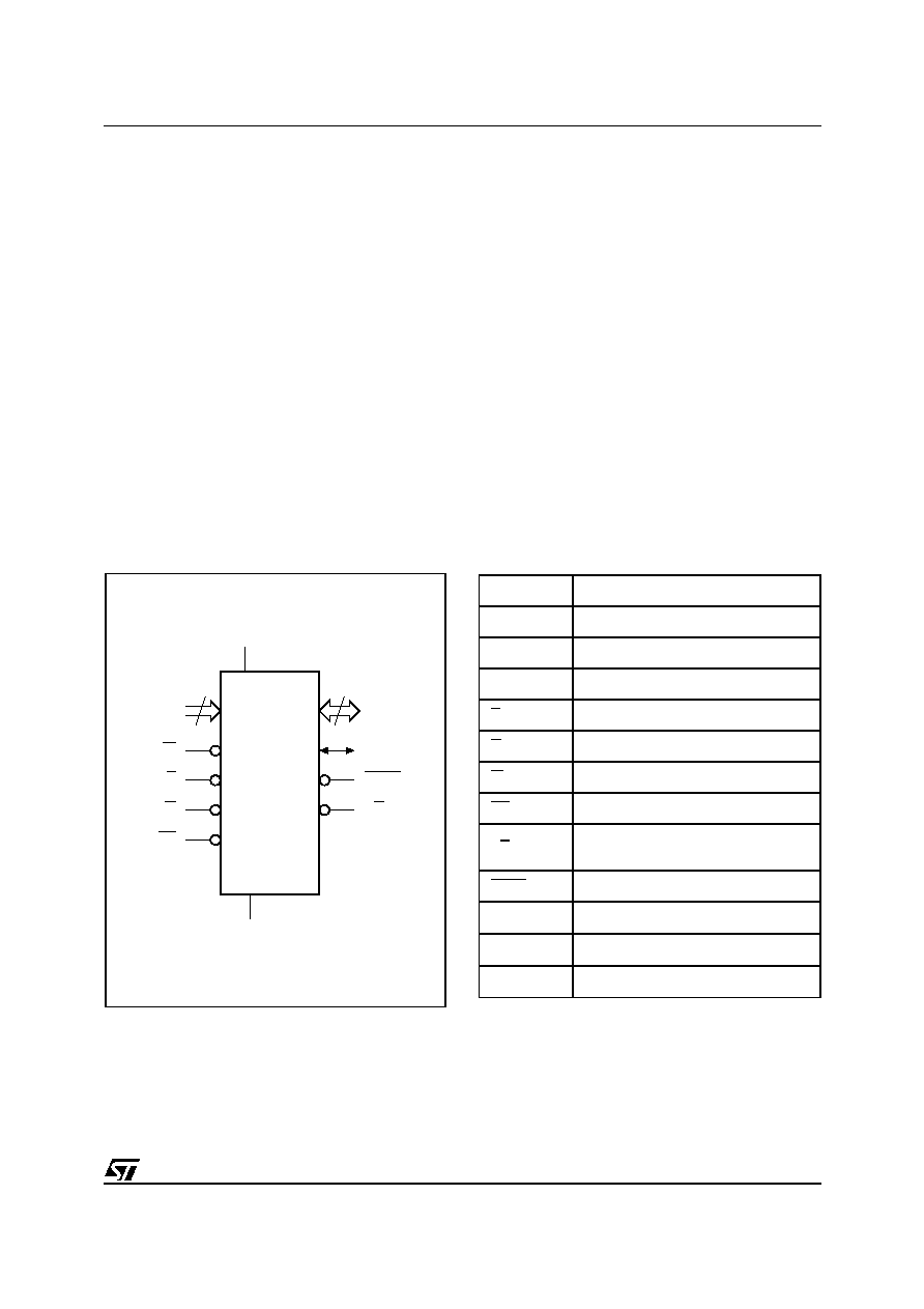
Chip Enable, Output Enable and Write Enable sig-
nals control the bus operation of the memory.
They allow simple connection to most micropro-
cessors, often without additional logic.
The memory is offered in SO44, TSOP48 (12 x
20mm) and TFBGA48 (0.8mm pitch) packages.
The memory is supplied with all the bits erased
(set to '1').
Figure 2. Logic Diagram
Table 1. Signal Names
AI06853
18
A0-A17
W
DQ0-DQ14
VCC
M29W400DT
M29W400DB
E
VSS
15
G
RP
DQ15A1
BYTE
RB
A0-A17
Address Inputs
DQ0-DQ7
Data Inputs/Outputs
DQ8-DQ14
Data Inputs/Outputs
DQ15A1
Data Input/Output or Address Input
E
Chip Enable
G
Output Enable
W
Write Enable
RP
Reset/Block Temporary Unprotect
RB
Ready/Busy Output
(not available on SO44 package)
BYTE
Byte/Word Organization Select
V
CC
Supply Voltage
V
SS
Ground
NC
Not Connected Internally
Document Outline
- FEATURES SUMMARY
- TABLE OF CONTENTS
- SUMMARY DESCRIPTION
- SIGNAL DESCRIPTIONS
- BUS OPERATIONS
- COMMAND INTERFACE
- STATUS REGISTER
- MAXIMUM RATING
- DC and AC PARAMETERS
- PACKAGE MECHANICAL
- Figure 16. SO44 - 44 lead Plastic Small Outline, 525 mils body width, Package Outline
- Table 16. SO44
44 lead Plastic Small Outline, 525 mils body width, Package Mechanical Data
- Figure 17. TSOP48
48 lead Plastic Thin Small Outline, 12 x 20mm, Package Outline
- Table 17. TSOP48
48 lead Plastic Thin Small Outline, 12 x 20mm, Package Mechanical Data
- Figure 18. TFBGA48 6x9mm
6x8 ball array
0.80mm pitch, Bottom View Package Outline
- Table 18. TFBGA48 6x9mm
6x8 active ball array
0.80mm pitch, Package Mechanical Data
- PART NUMBERING
- APPENDIX A. BLOCK ADDRESS TABLE
- APPENDIX B. BLOCK PROTECTION
- REVISION HISTORY