AI02065
18
A0-A17
W
DQ0-DQ14
VCC
M29W400T
M29W400B
E
VSS
15
G
RP
DQ15A≠1
BYTE
RB
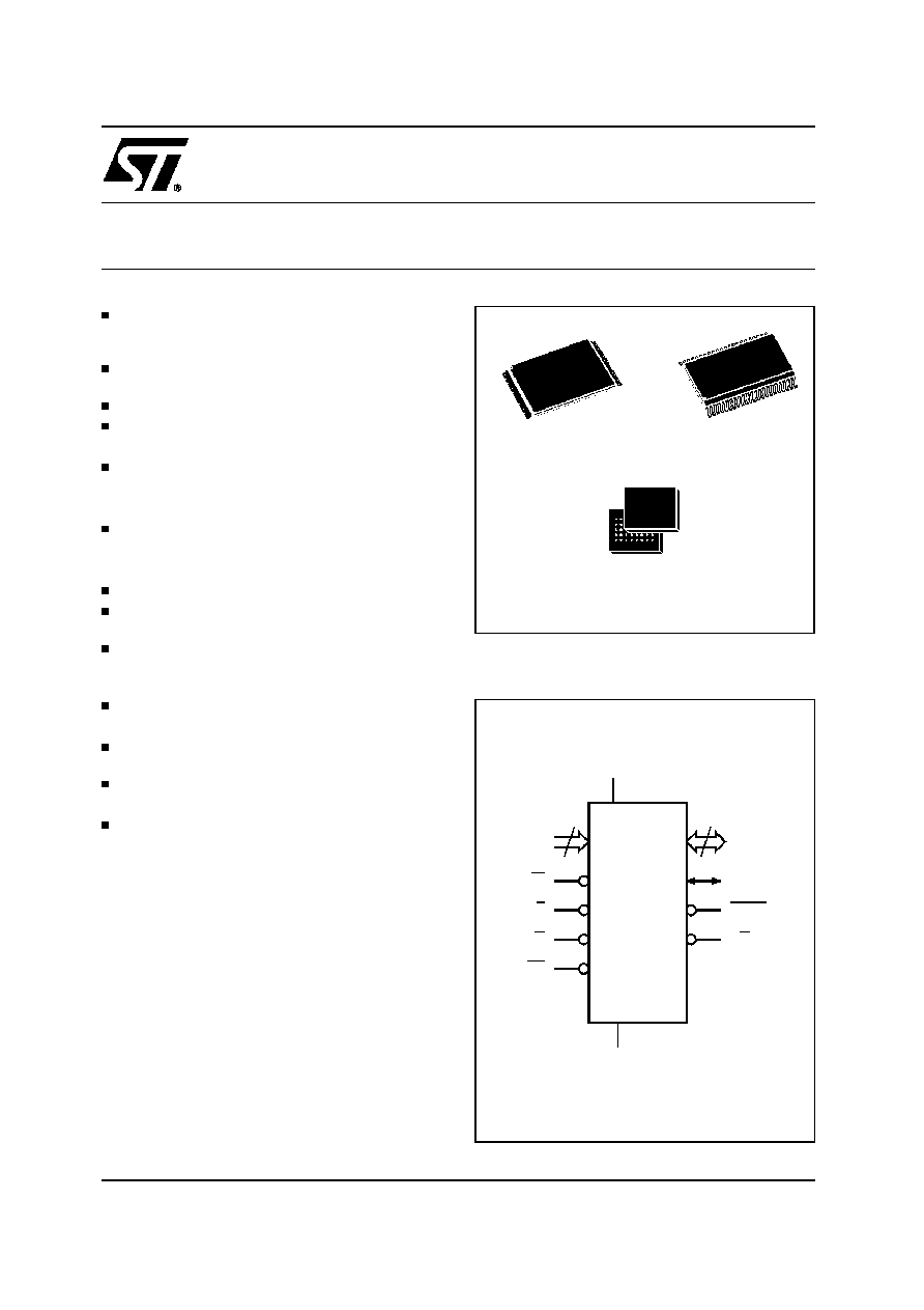
Figure 1. Logic Diagram
M29W400T
M29W400B
4 Mbit (512Kb x8 or 256Kb x16, Boot Block)
Low Voltage Single Supply Flash Memory
NOT FOR NEW DESIGN
M29W400T and M29W400B are replaced
respectively by the M29W400BT and
M29W400BB
2.7V to 3.6V SUPPLY VOLTAGE for
PROGRAM, ERASE and READ OPERATIONS
FAST ACCESS TIME: 90ns
FAST PROGRAMMING TIME
≠ 10
µ
s by Byte / 16
µ
s by Word typical
PROGRAM/ERASE CONTROLLER (P/E.C.)
≠ Program Byte-by-Byte or Word-by-Word
≠ Status Register bits and Ready/Busy Output
MEMORY BLOCKS
≠ Boot Block (Top or Bottom location)
≠ Parameter and Main blocks
BLOCK, MULTI-BLOCK and CHIP ERASE
MULTI BLOCK PROTECTION/TEMPORARY
UNPROTECTION MODES
ERASE SUSPEND and RESUME MODES
≠ Read and Program another Block during
Erase Suspend
LOW POWER CONSUMPTION
≠ Stand-by and Automatic Stand-by
100,000 PROGRAM/ERASE CYCLES per
BLOCK
20 YEARS DATA RETENTION
≠ Defectivity below 1ppm/year
ELECTRONIC SIGNATURE
≠ Manufacturer Code: 0020h
≠ Device Code, M29W400T: 00EEh
≠ Device Code, M29W400B: 00EFh
DESCRIPTION
The M29W400 is a non-volatile memory that may
be erased electrically at the block or chip level and
programmed in-system on a Byte-by-Byte or Word-
by-Word basis using only a single 2.7V to 3.6V V
CC
supply. For Program and Erase operations the
necessary high voltages are generated internally.
The device can also be programmed in standard
programmers.
The array matrix organisation allows each block to
be erased and reprogrammed without affecting
other blocks. Blocks can be protected against pro-
graming and erase on programming equipment,
November 1999
1/34
This is information on a product still in productionbut not recommended for new designs.
44
1
SO44 (M)
TSOP48 (N)
12 x 20 mm
BGA
FBGA48 (ZA)
8 x 6 solder balls

DQ3
DQ9
DQ2
A6
DQ0
W
A3
RB
DQ6
A8
A9
DQ13
A17
A10
DQ14
A2
DQ12
DQ10
DQ15A≠1
VCC
DQ4
DQ5
A7
DQ7
NC
NC
AI02066
M29W400T
M29W400B
(Normal)
12
1
13
24
25
36
37
48
DQ8
NC
NC
A1
NC
A4
A5
DQ1
DQ11
G
A12
A13
A16
A11
BYTE
A15
A14
VSS
E
A0
RP
VSS
Figure 2A. TSOP Pin Connections
G
DQ0
DQ8
A3
A0
E
VSS
A2
A1
A13
VSS
A14
A15
DQ7
A12
A16
BYTE
DQ15A≠1
DQ5
DQ2
DQ3
VCC
DQ11
DQ4
DQ14
A9
W
RB
A4
NC
RP
A7
AI02068
M29W400T
M29W400B
8
2
3
4
5
6
7
9
10
11
12
13
14
15
16
32
31
30
29
28
27
26
25
24
23
22
20
19
18
17
DQ1
DQ9
A6
A5
DQ6
DQ13
44
39
38
37
36
35
34
33
A11
A10
DQ10
21
DQ12
40
43
1
42
41
A17
A8
Figure 2C. SO Pin Connections
DQ3
DQ9
DQ2
DQ0
DQ6
DQ13
DQ14
DQ12
DQ10
DQ15A≠1
VCC
DQ4
DQ5
DQ7
AI02067
M29W400T
M29W400B
(Reverse)
12
1
13
24
25
36
37
48
DQ8
DQ1
DQ11
A16
BYTE
VSS
A0
VSS
A6
A3
A8
A9
A17
A10
A2
A7
NC
NC
NC
NC
A1
NC
A4
A5
A12
A13
A11
A15
A14
RP
W
RB
G
E
Figure 2B. TSOP Reverse Pin Connections
A0-A17
Address Inputs
DQ0-DQ7
Data Input/Outputs, Command Inputs
DQ8-DQ14
Data Input/Outputs
DQ15A≠1
Data Input/Output or Address Input
E
Chip Enable
G
Output Enable
W
Write Enable
RP
Reset / Block Temporary Unprotect
RB
Ready/Busy Output
BYTE
Byte/Word Organisation
V
CC
Supply Voltage
V
SS
Ground
Table 1. Signal Names
Warning: NC = Not Connected.
Warning: NC = Not Connected.
Warning: NC = Not Connected.
2/34
M29W400T, M29W400B
Symbol
Parameter
Value
Unit
T
A
Ambient Operating Temperature
(3)
≠40 to 85
∞
C
T
BIAS
Temperature Under Bias
≠50 to 125
∞
C
T
STG
Storage Temperature
≠65 to 150
∞
C
V
IO
(2)
Input or Output Voltages
≠0.6 to 5
V
V
CC
Supply Voltage
≠0.6 to 5
V
V
(A9, E, G, RP)
(2)
A9, E, G, RP Voltage
≠0.6 to 13.5
V
Notes: 1. Except for the rating "Operating Temperature Range", stresses above those listed in the Table "Absolute Maximum Ratings"
may cause permanent damage to the device. These are stress ratings only and operation of the device at these or any other
conditions above those indicated in the Operating sections of this specification is not implied. Exposure to Absolute Maximum
Rating conditions for extended periods may affect device reliability. Refer also to the STMicroelectronics SURE Program and other
relevant quality documents.
2. Minimum Voltage may undershoot to ≠2V during transition and for less than 20ns.
3. Depends on range.
Table 2. Absolute Maximum Ratings
(1)
DESCRIPTION (Cont'd)
AI00912
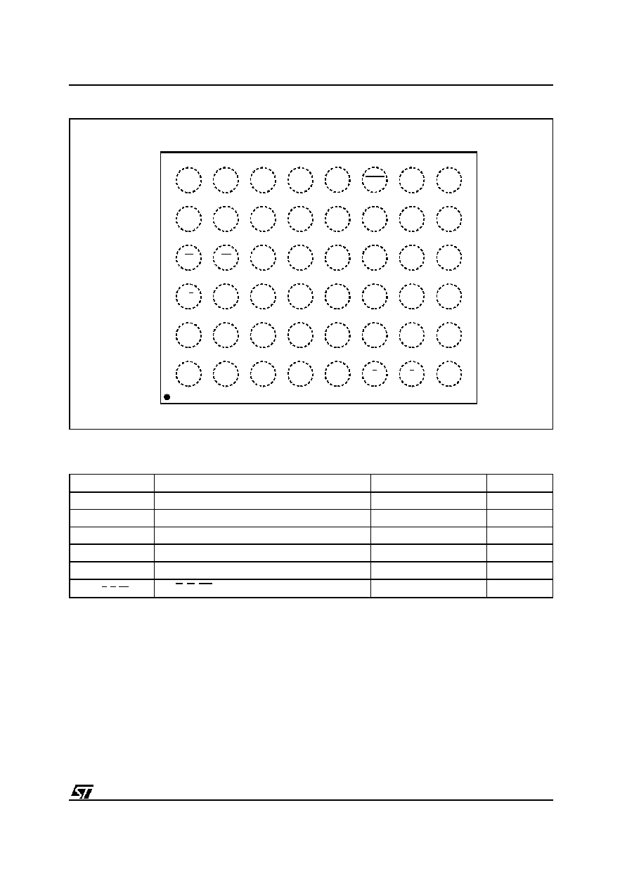
D
E
F
8
7
6
5
4
3
2
1
B
C
A
VSS
DQ15
A≠1
A15
A14
A12
A13
DQ3
DQ11
DQ10
NC
NC
RB
DQ1
DQ9
DQ8
DQ0
A6
A17
A7
G
E
A0
A4
A3
DQ2
DQ6
DQ13
DQ14
A10
A8
A9
DQ4
VCC
DQ12
DQ5
NC
NC
RP
W
A11
DQ7
A1
A2
VSS
A5
NC
A16
BYTE
Figure 2D. FBGA Package Ball Out (Top View)
Warning: NC = Not Connected.
and temporarily unprotected to make changes in
the application. Each block can be programmed
and erased over 100,000 cycles.
Instructions for Read/Reset, Auto Select for read-
ing the Electronic Signature or Block Protection
status, Programming, Block and Chip Erase, Erase
Suspend and Resume are written to the device in
cycles of commands to a Command Interface using
standard microprocessor write timings.
The device is offered in TSOP48 (12 x 20mm),
SO44 and FBGA48 (8 x 6 balls, 0.8mm pitch)
packages. Both normal and reverse pinouts are
available for the TSOP48 package.
3/34
M29W400T, M29W400B
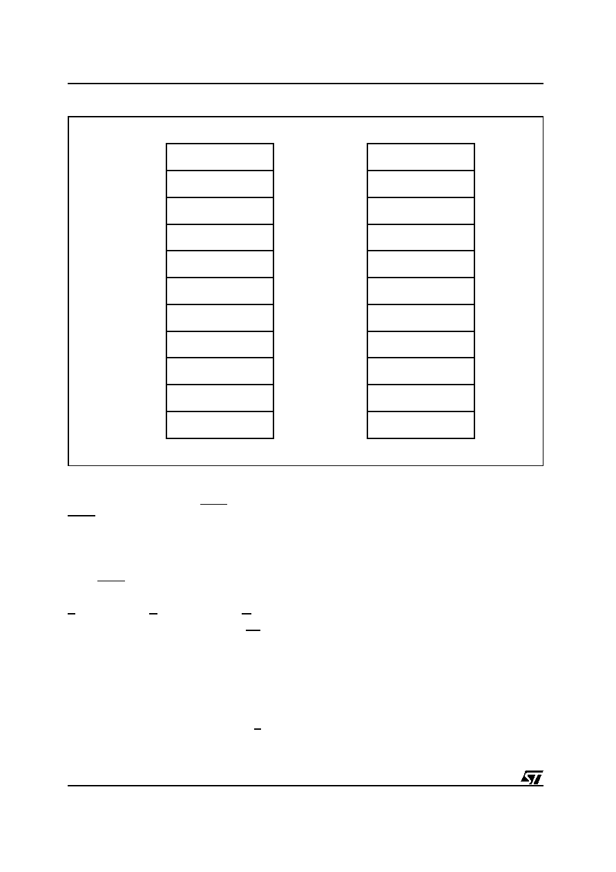
16K BOOT BLOCK
AI02090
7FFFFh
7C000h
7BFFFh
7A000h
79FFFh
40000h
3FFFFh
8K PARAMETER BLOCK
8K PARAMETER BLOCK
32K MAIN BLOCK
64K MAIN BLOCK
64K MAIN BLOCK
64K MAIN BLOCK
20000h
1FFFFh
10000h
0FFFFh
00000h
M29W400T
64K MAIN BLOCK
64K MAIN BLOCK
64K MAIN BLOCK
78000h
77FFFh
70000h
6FFFFh
60000h
5FFFFh
50000h
4FFFFh
M29W400B
16K BOOT BLOCK
8K PARAMETER BLOCK
8K PARAMETER BLOCK
32K MAIN BLOCK
64K MAIN BLOCK
64K MAIN BLOCK
64K MAIN BLOCK
64K MAIN BLOCK
64K MAIN BLOCK
64K MAIN BLOCK
40000h
3FFFFh
30000h
2FFFFh
20000h
1FFFFh
7FFFFh
70000h
6FFFFh
60000h
5FFFFh
50000h
4FFFFh
10000h
0FFFFh
08000h
07FFFh
04000h
03FFFh
00000h
64K MAIN BLOCK
06000h
05FFFh
64K MAIN BLOCK
30000h
2FFFFh
Figure 3. Memory Map and Block Address Table (x8)
Organisation
The M29W400 is organised as 512K x8 or 256K
x16 bits selectable by the BYTE signal. When
BYTE is Low the Byte-wide x8 organisation is
selected and the address lines are DQ15A≠1 and
A0-A17. The Data Input/Output signal DQ15A≠1
acts as address line A≠1 which selects the lower or
upper Byte of the memory word for output on
DQ0-DQ7, DQ8-DQ14 remain at High impedance.
When BYTE is High the memory uses the address
inputs A0-A17 and the Data Input/Outputs DQ0-
DQ15. Memory control is provided by Chip Enable
E, Output Enable G and Write Enable W inputs.
A Reset/Block Temporary Unprotection RP tri-level
input provides a hardware reset when pulled Low,
and when held High (at V
ID
) temporarily unprotects
blocks previously protected allowing them to be
programed and erased. Erase and Programopera-
tions are controlled by an internal Program/Erase
Controller (P/E.C.). Status Register data output on
DQ7 provides a Data Polling signal, and DQ6 and
DQ2 provide Toggle signals to indicate the state of
the P/E.C operations. A Ready/Busy RB output
indicates the completion of the internal algorithms.
Memory Blocks
The devices feature asymmetrically blocked archi-
tecture providing system memory integration. Both
M29W400Tand M29W400Bdevices have an array
of 11 blocks, one Boot Block of 16 KBytes or 8
KWords, two Parameter Blocks of 8 KBytes or 4
KWords, one Main Block of 32 KBytes or 16
KWords and seven Main Blocks of 64 KBytes or 32
KWords. The M29W400T has the Boot Block at the
top of the memory address space and the
M29W400B locates the Boot Block starting at the
bottom. The memory maps are showed in Figure
3. Each block can be erased separately, any com-
bination of blocks can be specified for multi-block
erase or the entire chip may be erased. The Erase
operations are managed automatically by the
P/E.C. The block erase operation can be sus-
pended in order to read from or program to any
block not being ersased, and then resumed.
Block protection provides additional data security.
Each block can be separately protected or unpro-
tected against Program or Erase on programming
equipment. All previously protected blocks can be
temporarily unprotected in the application.
4/34
M29W400T, M29W400B

Address Range (x8)
Address Range (x16)
A17
A16
A15
A14
A13
A12
00000h-03FFFh
00000h-01FFFh
0
0
0
0
0
X
04000h-05FFFh
02000h-02FFFh
0
0
0
0
1
0
06000h-07FFFh
03000h-03FFFh
0
0
0
0
1
1
08000h-0FFFFh
04000h-07FFFh
0
0
0
1
X
X
10000h-1FFFFh
08000h-0FFFFh
0
0
1
X
X
X
20000h-2FFFFh
10000h-17FFFh
0
1
0
X
X
X
30000h-3FFFFh
18000h-1FFFFh
0
1
1
X
X
X
40000h-4FFFFh
20000h-27FFFh
1
0
0
X
X
X
50000h-5FFFFh
28000h-2FFFFh
1
0
1
X
X
X
60000h-6FFFFh
30000h-37FFFh
1
1
0
X
X
X
70000h-7FFFFh
38000h-3FFFFh
1
1
1
X
X
X
Table 3B. M29W400B Block Address Table
Address Range (x8)
Address Range (x16)
A17
A16
A15
A14
A13
A12
00000h-0FFFFh
00000h-07FFFh
0
0
0
X
X
X
10000h-1FFFFh
08000h-0FFFFh
0
0
1
X
X
X
20000h-2FFFFh
10000h-17FFFh
0
1
0
X
X
X
30000h-3FFFFh
18000h-1FFFFh
0
1
1
X
X
X
40000h-4FFFFh
20000h-27FFFh
1
0
0
X
X
X
50000h-5FFFFh
28000h-2FFFFh
1
0
1
X
X
X
60000h-6FFFFh
30000h-37FFFh
1
1
0
X
X
X
70000h-77FFFh
38000h-3BFFFh
1
1
1
0
X
X
78000h-79FFFh
3C000h-3CFFFh
1
1
1
1
0
0
7A000h-7BFFFh
3D000h-3DFFFh
1
1
1
1
0
1
7C000h-7FFFFh
3E000h-3FFFFh
1
1
1
1
1
X
Table 3A. M29W400T Block Address Table
Bus Operations
The following operations can be performed using
the appropriate bus cycles: Read (Array, Electronic
Signature, Block Protection Status), Write com-
mand, Output Disable, Standby, Reset, Block Pro-
tection, Unprotection, Protection Verify, Unprotec-
tion Verify and Block Temporary Unprotection. See
Tables 4 and 5.
5/34
M29W400T, M29W400B