Äîêóìåíòàöèÿ è îïèñàíèÿ www.docs.chipfind.ru
1/49
December 2004
M29W640DT
M29W640DB
64 Mbit (8Mb x8 or 4Mb x16, Boot Block)
3V Supply Flash Memory
FEATURES SUMMARY
SUPPLY VOLTAGE
V
CC
=
2.7V to 3.6V for Program, Erase,
Read
V
PP
=12 V for Fast Program (optional)
ACCESS TIME: 90 ns
PROGRAMMING TIME
10 µs per Byte/Word typical
Double Word Programming Option
135 MEMORY BLOCKS
1 Boot Block and 7 Parameter Blocks,
8 KBytes each (Top or Bottom Location)
127 Main Blocks, 64 KBytes each
PROGRAM/ERASE CONTROLLER
Embedded Byte/Word Program
algorithms
ERASE SUSPEND and RESUME MODES
Read and Program another Block during
Erase Suspend
UNLOCK BYPASS PROGRAM COMMAND
Faster Production/Batch Programming
V
PP
/WP Pin for FAST PROGRAM and WRITE
PROTECT
TEMPORARY BLOCK UNPROTECTION
MODE
COMMON FLASH INTERFACE
64-bit Security Code
EXTENDED MEMORY BLOCK
Extra block used as security block or to
store additional information
LOW POWER CONSUMPTION
Standby and Automatic Standby
100,000 PROGRAM/ERASE CYCLES per
BLOCK
ELECTRONIC SIGNATURE
Manufacturer Code: 0020h
Top Device Code M29W640DT: 22DEh
Bottom Device Code M29W640DB:
22DFh
Figure 1. Packages
TSOP48 (N)
12 x 20mm
TFBGA63 (ZA)
63 ball array
FBGA

M29W640DT, M29W640DB
2/49
TABLE OF CONTENTS
FEATURES SUMMARY . . . . . . . . . . . . . . . . . . . . . . . . . . . . . . . . . . . . . . . . . . . . . . . . . . . . . . . . . . . . . 1
Figure 1. Packages . . . . . . . . . . . . . . . . . . . . . . . . . . . . . . . . . . . . . . . . . . . . . . . . . . . . . . . . . . . . . . 1
SUMMARY DESCRIPTION . . . . . . . . . . . . . . . . . . . . . . . . . . . . . . . . . . . . . . . . . . . . . . . . . . . . . . . . . . . 5
Figure 2. Logic Diagram . . . . . . . . . . . . . . . . . . . . . . . . . . . . . . . . . . . . . . . . . . . . . . . . . . . . . . . . . . 5
Table 1. Signal Names . . . . . . . . . . . . . . . . . . . . . . . . . . . . . . . . . . . . . . . . . . . . . . . . . . . . . . . . . . 5
Figure 3. TSOP Connections . . . . . . . . . . . . . . . . . . . . . . . . . . . . . . . . . . . . . . . . . . . . . . . . . . . . . . 6
Figure 4. TFBGA Connections (Top view through package) . . . . . . . . . . . . . . . . . . . . . . . . . . . . . . 7
SIGNAL DESCRIPTIONS . . . . . . . . . . . . . . . . . . . . . . . . . . . . . . . . . . . . . . . . . . . . . . . . . . . . . . . . . . . . 8
Address Inputs (A0-A21). . . . . . . . . . . . . . . . . . . . . . . . . . . . . . . . . . . . . . . . . . . . . . . . . . . . . . . . . . 8
Data Inputs/Outputs (DQ0-DQ7). . . . . . . . . . . . . . . . . . . . . . . . . . . . . . . . . . . . . . . . . . . . . . . . . . . . 8
Data Inputs/Outputs (DQ8-DQ14). . . . . . . . . . . . . . . . . . . . . . . . . . . . . . . . . . . . . . . . . . . . . . . . . . . 8
Data Input/Output or Address Input (DQ15A1).. . . . . . . . . . . . . . . . . . . . . . . . . . . . . . . . . . . . . . . . 8
Chip Enable (E). . . . . . . . . . . . . . . . . . . . . . . . . . . . . . . . . . . . . . . . . . . . . . . . . . . . . . . . . . . . . . . . . 8
Output Enable (G). . . . . . . . . . . . . . . . . . . . . . . . . . . . . . . . . . . . . . . . . . . . . . . . . . . . . . . . . . . . . . . 8
Write Enable (W). . . . . . . . . . . . . . . . . . . . . . . . . . . . . . . . . . . . . . . . . . . . . . . . . . . . . . . . . . . . . . . . 8
V
PP/
Write Protect (V
PP/
WP). . . . . . . . . . . . . . . . . . . . . . . . . . . . . . . . . . . . . . . . . . . . . . . . . . . . . . . . 8
Reset/Block Temporary Unprotect (RP). . . . . . . . . . . . . . . . . . . . . . . . . . . . . . . . . . . . . . . . . . . . . . . 8
Ready/Busy Output (RB). . . . . . . . . . . . . . . . . . . . . . . . . . . . . . . . . . . . . . . . . . . . . . . . . . . . . . . . . . 8
Byte/Word Organization Select (BYTE). . . . . . . . . . . . . . . . . . . . . . . . . . . . . . . . . . . . . . . . . . . . . . . 9
V
CC
Supply Voltage (2.7V to 3.6V).. . . . . . . . . . . . . . . . . . . . . . . . . . . . . . . . . . . . . . . . . . . . . . . . . . 9
V
SS
Ground. . . . . . . . . . . . . . . . . . . . . . . . . . . . . . . . . . . . . . . . . . . . . . . . . . . . . . . . . . . . . . . . . . . . 9
BUS OPERATIONS. . . . . . . . . . . . . . . . . . . . . . . . . . . . . . . . . . . . . . . . . . . . . . . . . . . . . . . . . . . . . . . . 10
Bus Read. . . . . . . . . . . . . . . . . . . . . . . . . . . . . . . . . . . . . . . . . . . . . . . . . . . . . . . . . . . . . . . . . . . . . 10
Bus Write. . . . . . . . . . . . . . . . . . . . . . . . . . . . . . . . . . . . . . . . . . . . . . . . . . . . . . . . . . . . . . . . . . . . . 10
Output Disable. . . . . . . . . . . . . . . . . . . . . . . . . . . . . . . . . . . . . . . . . . . . . . . . . . . . . . . . . . . . . . . . . 10
Standby. . . . . . . . . . . . . . . . . . . . . . . . . . . . . . . . . . . . . . . . . . . . . . . . . . . . . . . . . . . . . . . . . . . . . . 10
Automatic Standby. . . . . . . . . . . . . . . . . . . . . . . . . . . . . . . . . . . . . . . . . . . . . . . . . . . . . . . . . . . . . . 10
Special Bus Operations . . . . . . . . . . . . . . . . . . . . . . . . . . . . . . . . . . . . . . . . . . . . . . . . . . . . . . . . 10
Electronic Signature. . . . . . . . . . . . . . . . . . . . . . . . . . . . . . . . . . . . . . . . . . . . . . . . . . . . . . . . . . . . . 10
Block Protect and Chip Unprotect. . . . . . . . . . . . . . . . . . . . . . . . . . . . . . . . . . . . . . . . . . . . . . . . . . 10
Table 2. Bus Operations, BYTE = V
IL
. . . . . . . . . . . . . . . . . . . . . . . . . . . . . . . . . . . . . . . . . . . . . . 10
Table 3. Bus Operations, BYTE = V
IH
. . . . . . . . . . . . . . . . . . . . . . . . . . . . . . . . . . . . . . . . . . . . . . 11
COMMAND INTERFACE . . . . . . . . . . . . . . . . . . . . . . . . . . . . . . . . . . . . . . . . . . . . . . . . . . . . . . . . . . . 12
Read/Reset Command. . . . . . . . . . . . . . . . . . . . . . . . . . . . . . . . . . . . . . . . . . . . . . . . . . . . . . . . . . 12
Auto Select Command. . . . . . . . . . . . . . . . . . . . . . . . . . . . . . . . . . . . . . . . . . . . . . . . . . . . . . . . . . 12
Read CFI Query Command . . . . . . . . . . . . . . . . . . . . . . . . . . . . . . . . . . . . . . . . . . . . . . . . . . . . . . 12
Program Command. . . . . . . . . . . . . . . . . . . . . . . . . . . . . . . . . . . . . . . . . . . . . . . . . . . . . . . . . . . . 12
Fast Program Commands . . . . . . . . . . . . . . . . . . . . . . . . . . . . . . . . . . . . . . . . . . . . . . . . . . . . . . . 12
Quadruple Byte Program Command. . . . . . . . . . . . . . . . . . . . . . . . . . . . . . . . . . . . . . . . . . . . . . . . 13

3/49
M29W640DT, M29W640DB
Double Word Program Command. . . . . . . . . . . . . . . . . . . . . . . . . . . . . . . . . . . . . . . . . . . . . . . . . . 13
Unlock Bypass Command. . . . . . . . . . . . . . . . . . . . . . . . . . . . . . . . . . . . . . . . . . . . . . . . . . . . . . . 13
Unlock Bypass Program Command. . . . . . . . . . . . . . . . . . . . . . . . . . . . . . . . . . . . . . . . . . . . . . . 13
Unlock Bypass Reset Command. . . . . . . . . . . . . . . . . . . . . . . . . . . . . . . . . . . . . . . . . . . . . . . . . 13
Chip Erase Command. . . . . . . . . . . . . . . . . . . . . . . . . . . . . . . . . . . . . . . . . . . . . . . . . . . . . . . . . . 13
Block Erase Command. . . . . . . . . . . . . . . . . . . . . . . . . . . . . . . . . . . . . . . . . . . . . . . . . . . . . . . . . 14
Erase Suspend Command. . . . . . . . . . . . . . . . . . . . . . . . . . . . . . . . . . . . . . . . . . . . . . . . . . . . . . . 14
Erase Resume Command. . . . . . . . . . . . . . . . . . . . . . . . . . . . . . . . . . . . . . . . . . . . . . . . . . . . . . . 14
Enter Extended Block Command . . . . . . . . . . . . . . . . . . . . . . . . . . . . . . . . . . . . . . . . . . . . . . . . . 14
Exit Extended Block Command . . . . . . . . . . . . . . . . . . . . . . . . . . . . . . . . . . . . . . . . . . . . . . . . . . 15
Block Protect and Chip Unprotect Commands . . . . . . . . . . . . . . . . . . . . . . . . . . . . . . . . . . . . . 15
Table 4. Commands, 16-bit mode, BYTE = V
IH
. . . . . . . . . . . . . . . . . . . . . . . . . . . . . . . . . . . . . . . 15
Table 5. Commands, 8-bit mode, BYTE = V
IL
. . . . . . . . . . . . . . . . . . . . . . . . . . . . . . . . . . . . . . . . 15
Table 6. Program, Erase Times and Program, Erase Endurance Cycles . . . . . . . . . . . . . . . . . . . 16
STATUS REGISTER . . . . . . . . . . . . . . . . . . . . . . . . . . . . . . . . . . . . . . . . . . . . . . . . . . . . . . . . . . . . . . . 17
Data Polling Bit (DQ7). . . . . . . . . . . . . . . . . . . . . . . . . . . . . . . . . . . . . . . . . . . . . . . . . . . . . . . . . . . 17
Toggle Bit (DQ6).. . . . . . . . . . . . . . . . . . . . . . . . . . . . . . . . . . . . . . . . . . . . . . . . . . . . . . . . . . . . . . . 17
Error Bit (DQ5). . . . . . . . . . . . . . . . . . . . . . . . . . . . . . . . . . . . . . . . . . . . . . . . . . . . . . . . . . . . . . . . . 17
Erase Timer Bit (DQ3). . . . . . . . . . . . . . . . . . . . . . . . . . . . . . . . . . . . . . . . . . . . . . . . . . . . . . . . . . . 17
Alternative Toggle Bit (DQ2).. . . . . . . . . . . . . . . . . . . . . . . . . . . . . . . . . . . . . . . . . . . . . . . . . . . . . . 17
Table 7. Status Register Bits . . . . . . . . . . . . . . . . . . . . . . . . . . . . . . . . . . . . . . . . . . . . . . . . . . . . . 18
Figure 5. Data Polling Flowchart. . . . . . . . . . . . . . . . . . . . . . . . . . . . . . . . . . . . . . . . . . . . . . . . . . . 18
Figure 6. Data Toggle Flowchart. . . . . . . . . . . . . . . . . . . . . . . . . . . . . . . . . . . . . . . . . . . . . . . . . . . 18
MAXIMUM RATING. . . . . . . . . . . . . . . . . . . . . . . . . . . . . . . . . . . . . . . . . . . . . . . . . . . . . . . . . . . . . . . . 19
Table 8. Absolute Maximum Ratings . . . . . . . . . . . . . . . . . . . . . . . . . . . . . . . . . . . . . . . . . . . . . . . 19
DC and AC PARAMETERS . . . . . . . . . . . . . . . . . . . . . . . . . . . . . . . . . . . . . . . . . . . . . . . . . . . . . . . . . 20
Table 9. Operating and AC Measurement Conditions . . . . . . . . . . . . . . . . . . . . . . . . . . . . . . . . . . 20
Figure 7. AC Measurement I/O Waveform . . . . . . . . . . . . . . . . . . . . . . . . . . . . . . . . . . . . . . . . . . . 20
Figure 8. AC Measurement Load Circuit. . . . . . . . . . . . . . . . . . . . . . . . . . . . . . . . . . . . . . . . . . . . . 20
Table 10. Device Capacitance. . . . . . . . . . . . . . . . . . . . . . . . . . . . . . . . . . . . . . . . . . . . . . . . . . . . . 20
Table 11. DC Characteristics. . . . . . . . . . . . . . . . . . . . . . . . . . . . . . . . . . . . . . . . . . . . . . . . . . . . . . 21
Figure 9. Read Mode AC Waveforms . . . . . . . . . . . . . . . . . . . . . . . . . . . . . . . . . . . . . . . . . . . . . . . 22
Table 12. Read AC Characteristics . . . . . . . . . . . . . . . . . . . . . . . . . . . . . . . . . . . . . . . . . . . . . . . . . 22
Figure 10.Write AC Waveforms, Write Enable Controlled . . . . . . . . . . . . . . . . . . . . . . . . . . . . . . . . 23
Table 13. Write AC Characteristics, Write Enable Controlled . . . . . . . . . . . . . . . . . . . . . . . . . . . . . 23
Figure 11.Write AC Waveforms, Chip Enable Controlled . . . . . . . . . . . . . . . . . . . . . . . . . . . . . . . . 24
Table 14. Write AC Characteristics, Chip Enable Controlled. . . . . . . . . . . . . . . . . . . . . . . . . . . . . . 24
Figure 12.Reset/Block Temporary Unprotect AC Waveforms . . . . . . . . . . . . . . . . . . . . . . . . . . . . . 25
Table 15. Reset/Block Temporary Unprotect AC Characteristics . . . . . . . . . . . . . . . . . . . . . . . . . . 25
Figure 13.Accelerated Program Timing Waveforms . . . . . . . . . . . . . . . . . . . . . . . . . . . . . . . . . . . . 25
PACKAGE MECHANICAL . . . . . . . . . . . . . . . . . . . . . . . . . . . . . . . . . . . . . . . . . . . . . . . . . . . . . . . . . . 26
Figure 14.TSOP48 48 lead Plastic Thin Small Outline, 12 x 20mm, Package Outline. . . . . . . . . 26

M29W640DT, M29W640DB
4/49
Table 16. TSOP48 48 lead Plastic Thin Small Outline, 12 x 20mm, Package Mechanical Data . 26
Figure 15.TFBGA63 7x11mm - 6x8 active ball array, 0.8mm pitch, Package Outline. . . . . . . . . . . 27
Table 17. TFBGA63 7x11mm - 6x8 active ball array, 0.8mm pitch, Package Mechanical Data . . . 27
PART NUMBERING . . . . . . . . . . . . . . . . . . . . . . . . . . . . . . . . . . . . . . . . . . . . . . . . . . . . . . . . . . . . . . . 28
Table 18. Ordering Information Scheme . . . . . . . . . . . . . . . . . . . . . . . . . . . . . . . . . . . . . . . . . . . . . 28
APPENDIX A.BLOCK ADDRESSES . . . . . . . . . . . . . . . . . . . . . . . . . . . . . . . . . . . . . . . . . . . . . . . . . . 29
Table 19. Top Boot Block Addresses, M29W640DT . . . . . . . . . . . . . . . . . . . . . . . . . . . . . . . . . . . . 29
Table 20. Bottom Boot Block Addresses, M29W640DB . . . . . . . . . . . . . . . . . . . . . . . . . . . . . . . . . 33
APPENDIX B.COMMON FLASH INTERFACE (CFI) . . . . . . . . . . . . . . . . . . . . . . . . . . . . . . . . . . . . . . 38
Table 21. Query Structure Overview . . . . . . . . . . . . . . . . . . . . . . . . . . . . . . . . . . . . . . . . . . . . . . . . 38
Table 22. CFI Query Identification String. . . . . . . . . . . . . . . . . . . . . . . . . . . . . . . . . . . . . . . . . . . . . 38
Table 23. CFI Query System Interface Information . . . . . . . . . . . . . . . . . . . . . . . . . . . . . . . . . . . . . 39
Table 24. Device Geometry Definition . . . . . . . . . . . . . . . . . . . . . . . . . . . . . . . . . . . . . . . . . . . . . . 39
Table 25. Primary Algorithm-Specific Extended Query Table . . . . . . . . . . . . . . . . . . . . . . . . . . . . . 40
Table 26. Security Code Area . . . . . . . . . . . . . . . . . . . . . . . . . . . . . . . . . . . . . . . . . . . . . . . . . . . . . 41
APPENDIX C.EXTENDED MEMORY BLOCK . . . . . . . . . . . . . . . . . . . . . . . . . . . . . . . . . . . . . . . . . . . 42
Factory Locked Extended Block . . . . . . . . . . . . . . . . . . . . . . . . . . . . . . . . . . . . . . . . . . . . . . . . . 42
Customer Lockable Extended Block . . . . . . . . . . . . . . . . . . . . . . . . . . . . . . . . . . . . . . . . . . . . . . 42
Table 27. Extended Block Address and Data . . . . . . . . . . . . . . . . . . . . . . . . . . . . . . . . . . . . . . . . . 42
APPENDIX D.BLOCK PROTECTION. . . . . . . . . . . . . . . . . . . . . . . . . . . . . . . . . . . . . . . . . . . . . . . . . . 43
Programmer Technique . . . . . . . . . . . . . . . . . . . . . . . . . . . . . . . . . . . . . . . . . . . . . . . . . . . . . . . . 43
In-System Technique . . . . . . . . . . . . . . . . . . . . . . . . . . . . . . . . . . . . . . . . . . . . . . . . . . . . . . . . . . 43
Table 28. Programmer Technique Bus Operations, BYTE = V
IH
or V
IL . . . . . . . . . . . . . . . . . . . . . . . . . . . 43
Figure 16.Programmer Equipment Group Protect Flowchart . . . . . . . . . . . . . . . . . . . . . . . . . . . . . 44
Figure 17.Programmer Equipment Chip Unprotect Flowchart. . . . . . . . . . . . . . . . . . . . . . . . . . . . . 45
Figure 18.In-System Equipment Group Protect Flowchart . . . . . . . . . . . . . . . . . . . . . . . . . . . . . . . 46
Figure 19.In-System Equipment Chip Unprotect Flowchart . . . . . . . . . . . . . . . . . . . . . . . . . . . . . . 47
REVISION HISTORY . . . . . . . . . . . . . . . . . . . . . . . . . . . . . . . . . . . . . . . . . . . . . . . . . . . . . . . . . . . . . . . 48
Table 29. Document Revision History . . . . . . . . . . . . . . . . . . . . . . . . . . . . . . . . . . . . . . . . . . . . . . . 48
5/49
M29W640DT, M29W640DB
SUMMARY DESCRIPTION
The M29W640D is a 64 Mbit (8Mb x8 or 4Mb x16)
non-volatile memory that can be read, erased and
reprogrammed. These operations can be per-
formed using a single low voltage (2.7 to 3.6V)
supply. On power-up the memory defaults to its
Read mode.
The memory is divided into blocks that can be
erased independently so it is possible to preserve
valid data while old data is erased. Blocks can be
protected in units of 256 KByte (generally groups
of four 64 KByte blocks), to prevent accidental
Program or Erase commands from modifying the
memory. Program and Erase commands are writ-
ten to the Command Interface of the memory. An
on-chip Program/Erase Controller simplifies the
process of programming or erasing the memory by
taking care of all of the special operations that are
required to update the memory contents. The end
of a program or erase operation can be detected
and any error conditions identified. The command
set required to control the memory is consistent
with JEDEC standards.
The device features an asymmetrical blocked ar-
chitecture. The device has an array of 135 blocks:
8 Parameters Blocks of 8 KBytes each (or
4 KWords each)
127 Main Blocks of 64 KBytes each (or
32 KWords each)
M29W640DT has the Parameter Blocks at the top
of the memory address space while the
M29W640DB locates the Parameter Blocks start-
ing from the bottom.
The M29W640D has an extra block, the Extended
Block, (of 32 KWords in x16 mode or of 64 KBytes
in x8 mode) that can be accessed using a dedicat-
ed command. The Extended Block can be protect-
ed and so is useful for storing security information.
However the protection is not reversible, once pro-
tected the protection cannot be undone.
Chip Enable, Output Enable and Write Enable sig-
nals control the bus operation of the memory.
They allow simple connection to most micropro-
cessors, often without additional logic.
The V
PP
/WP signal is used to enable faster pro-
gramming of the device, enabling double word
programming. If this signal is held at V
SS
, the boot
block, and its adjacent parameter block, are pro-
tected from program and erase operations.
The memory is delivered with all the bits erased (set
to 1).
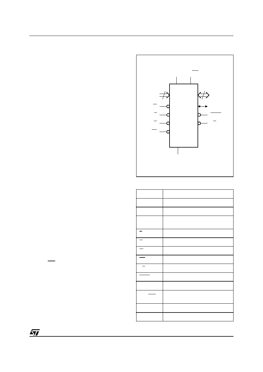
Figure 2. Logic Diagram
Table 1. Signal Names
A0-A21
Address Inputs
DQ0-DQ7
Data Inputs/Outputs
DQ8-DQ14
Data Inputs/Outputs
DQ15A1
(or DQ15)
Data Input/Output or Address Input
(or Data Input/Output)
E
Chip Enable
G
Output Enable
W
Write Enable
RP
Reset/Block Temporary Unprotect
RB
Ready/Busy Output
BYTE
Byte/Word Organization Select
V
CC
Supply Voltage
V
PP
/WP
Supply Voltage for Fast Program
(optional) or Write Protect
V
SS
Ground
NC
Not Connected Internally
AI05733
22
A0-A21
W
DQ0-DQ14
VCC
M29W640DT
M29W640DB
E
VSS
15
G
RP
DQ15A1
BYTE
RB
VPP/WP
Document Outline