Rev3
December 2005
1/72
1
M29W640FT
M29W640FB
64 Mbit (8Mb x8 or 4Mb x16, Page, Boot Block)
3V Supply Flash Memory
Features summary
Supply Voltage
≠
V
CC
= 2.7V to 3.6V for Program, Erase,
Read
≠
V
PP
=12 V for Fast Program (optional)
Asynchronous Random/Page Read
≠
Page Width: 4 Words
≠
Page Access: 25ns
≠
Random Access: 60ns, 70ns
Programming Time
≠
10
µ
s per Byte/Word typical
≠
4 Words/8 Bytes Program
135 memory blocks
≠
1 Boot Block and 7 Parameter Blocks,
8 KBytes each (Top or Bottom Location)
≠
127 Main Blocks, 64 KBytes each
Program/Erase Controller
≠
Embedded Byte/Word Program algorithms
Program/Erase Suspend and Resume
≠
Read from any Block during Program
Suspend
≠
Read and Program another Block during
Erase Suspend
Unlock Bypass Program command
≠
Faster Production/Batch Programming
V
PP
/WP pin for Fast Program and Write Protect
Temporary Block Unprotection mode
Common Flash Interface
≠
64-bit Security Code
Extended Memory Block
≠
Extra block used as security block or to
store additional information
Low power consumption
≠
Standby and Automatic Standby
100,000 Program/Erase cycles per block
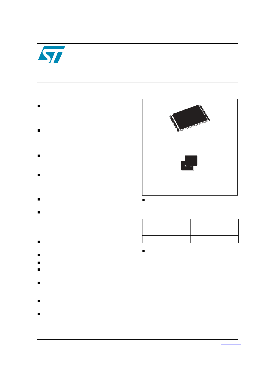
Figure 1.
Packages
Electronic Signature
≠
Manufacturer Code: 0020h
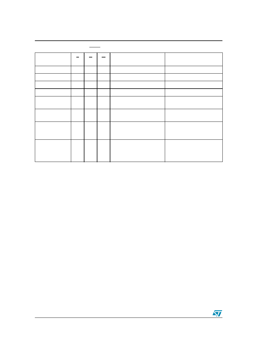
Table 1.
Device Codes
ECOPACK
Æ
packages
Root Part Number
Device Code
M29W640FT
22EDh
M29W640FB
22FDh
FBGA
TSOP48 (N)
12 x 20mm
TFBGA48 (ZA)
6x8mm
www.st.com

M29W640FT, M29W640FB
2/72
Contents
1
Summary description . . . . . . . . . . . . . . . . . . . . . . . . . . . . . . . . . . . . . . . . . . 7
2
Signal descriptions . . . . . . . . . . . . . . . . . . . . . . . . . . . . . . . . . . . . . . . . . . . 11
2.1
Address Inputs (A0-A21) . . . . . . . . . . . . . . . . . . . . . . . . . . . . . . . . . . . . . . . . 11
2.2
Data Inputs/Outputs (DQ0-DQ7) . . . . . . . . . . . . . . . . . . . . . . . . . . . . . . . . . . 11
2.3
Data Inputs/Outputs (DQ8-DQ14) . . . . . . . . . . . . . . . . . . . . . . . . . . . . . . . . . 11
2.4
Data Input/Output or Address Input (DQ15A
≠
1) . . . . . . . . . . . . . . . . . . . . . . 11
2.5
Chip Enable (E) . . . . . . . . . . . . . . . . . . . . . . . . . . . . . . . . . . . . . . . . . . . . . . . 11
2.6
Output Enable (G) . . . . . . . . . . . . . . . . . . . . . . . . . . . . . . . . . . . . . . . . . . . . . 11
2.7
Write Enable (W) . . . . . . . . . . . . . . . . . . . . . . . . . . . . . . . . . . . . . . . . . . . . . . 12
2.8
V
PP
/Write Protect (V
PP/
WP) . . . . . . . . . . . . . . . . . . . . . . . . . . . . . . . . . . . . . 12
2.9
Reset/Block Temporary Unprotect (RP) . . . . . . . . . . . . . . . . . . . . . . . . . . . . 13
2.10
Ready/Busy Output (RB) . . . . . . . . . . . . . . . . . . . . . . . . . . . . . . . . . . . . . . . 13
2.11
Byte/Word Organization Select (BYTE) . . . . . . . . . . . . . . . . . . . . . . . . . . . . 13
2.12
V
CC
Supply Voltage (2.7V to 3.6V) . . . . . . . . . . . . . . . . . . . . . . . . . . . . . . . . 13
2.13
V
SS
Ground . . . . . . . . . . . . . . . . . . . . . . . . . . . . . . . . . . . . . . . . . . . . . . . . . . 14
3
Bus operations . . . . . . . . . . . . . . . . . . . . . . . . . . . . . . . . . . . . . . . . . . . . . . 15
3.1
Bus Read . . . . . . . . . . . . . . . . . . . . . . . . . . . . . . . . . . . . . . . . . . . . . . . . . . . 15
3.2
Bus Write . . . . . . . . . . . . . . . . . . . . . . . . . . . . . . . . . . . . . . . . . . . . . . . . . . . 15
3.3
Output Disable . . . . . . . . . . . . . . . . . . . . . . . . . . . . . . . . . . . . . . . . . . . . . . . 15
3.4
Standby . . . . . . . . . . . . . . . . . . . . . . . . . . . . . . . . . . . . . . . . . . . . . . . . . . . . . 15
3.5
Automatic Standby . . . . . . . . . . . . . . . . . . . . . . . . . . . . . . . . . . . . . . . . . . . . 16
3.6
Special Bus Operations . . . . . . . . . . . . . . . . . . . . . . . . . . . . . . . . . . . . . . . . 16
3.6.1
Electronic Signature . . . . . . . . . . . . . . . . . . . . . . . . . . . . . . . . . . . . . . . . . . . 16
3.6.2
Block Protect and Chip Unprotect . . . . . . . . . . . . . . . . . . . . . . . . . . . . . . . . . 16
4
Command Interface . . . . . . . . . . . . . . . . . . . . . . . . . . . . . . . . . . . . . . . . . . . 19
4.1
Standard commands . . . . . . . . . . . . . . . . . . . . . . . . . . . . . . . . . . . . . . . . . . . 19
4.1.1
Read/Reset command . . . . . . . . . . . . . . . . . . . . . . . . . . . . . . . . . . . . . . . . . . 19
4.1.2
Auto Select command . . . . . . . . . . . . . . . . . . . . . . . . . . . . . . . . . . . . . . . . . . 19
4.1.3
Read CFI Query command . . . . . . . . . . . . . . . . . . . . . . . . . . . . . . . . . . . . . . 20

M29W640FT, M29W640FB
3/72
4.1.4
Chip Erase command . . . . . . . . . . . . . . . . . . . . . . . . . . . . . . . . . . . . . . . . . . 20
4.1.5
Block Erase command . . . . . . . . . . . . . . . . . . . . . . . . . . . . . . . . . . . . . . . . . . 20
4.1.6
Erase Suspend command . . . . . . . . . . . . . . . . . . . . . . . . . . . . . . . . . . . . . . . 21
4.1.7
Erase Resume command . . . . . . . . . . . . . . . . . . . . . . . . . . . . . . . . . . . . . . . 21
4.1.8
Program Suspend command . . . . . . . . . . . . . . . . . . . . . . . . . . . . . . . . . . . . . 21
4.1.9
Program Resume command . . . . . . . . . . . . . . . . . . . . . . . . . . . . . . . . . . . . . 22
4.1.10 Program command . . . . . . . . . . . . . . . . . . . . . . . . . . . . . . . . . . . . . . . . . . . . 22
4.2
Fast Program commands . . . . . . . . . . . . . . . . . . . . . . . . . . . . . . . . . . . . . . . 23
4.2.1
Double Byte Program command . . . . . . . . . . . . . . . . . . . . . . . . . . . . . . . . . . 23
4.2.2
Quadruple Byte Program command . . . . . . . . . . . . . . . . . . . . . . . . . . . . . . . 23
4.2.3
Octuple Byte Program command . . . . . . . . . . . . . . . . . . . . . . . . . . . . . . . . . 24
4.2.4
Double Word Program command . . . . . . . . . . . . . . . . . . . . . . . . . . . . . . . . . 24
4.2.5
Quadruple Word Program command . . . . . . . . . . . . . . . . . . . . . . . . . . . . . . . 25
4.2.6
Unlock Bypass command . . . . . . . . . . . . . . . . . . . . . . . . . . . . . . . . . . . . . . . 25
4.2.7
Unlock Bypass Program command . . . . . . . . . . . . . . . . . . . . . . . . . . . . . . . . 25
4.2.8
Unlock Bypass Reset command . . . . . . . . . . . . . . . . . . . . . . . . . . . . . . . . . . 25
4.3
Block Protection commands . . . . . . . . . . . . . . . . . . . . . . . . . . . . . . . . . . . . . 26
4.3.1
Enter Extended Block command . . . . . . . . . . . . . . . . . . . . . . . . . . . . . . . . . . 26
4.3.2
Exit Extended Block command . . . . . . . . . . . . . . . . . . . . . . . . . . . . . . . . . . . 26
4.3.3
Block Protect and Chip Unprotect commands . . . . . . . . . . . . . . . . . . . . . . . . 27
5
Status Register . . . . . . . . . . . . . . . . . . . . . . . . . . . . . . . . . . . . . . . . . . . . . . 30
5.1
Data Polling Bit (DQ7) . . . . . . . . . . . . . . . . . . . . . . . . . . . . . . . . . . . . . . . . . . 30
5.2
Toggle Bit (DQ6) . . . . . . . . . . . . . . . . . . . . . . . . . . . . . . . . . . . . . . . . . . . . . . 30
5.3
Error Bit (DQ5) . . . . . . . . . . . . . . . . . . . . . . . . . . . . . . . . . . . . . . . . . . . . . . . 31
5.4
Erase Timer Bit (DQ3) . . . . . . . . . . . . . . . . . . . . . . . . . . . . . . . . . . . . . . . . . 31
5.5
Alternative Toggle Bit (DQ2) . . . . . . . . . . . . . . . . . . . . . . . . . . . . . . . . . . . . . 31
6
Maximum rating . . . . . . . . . . . . . . . . . . . . . . . . . . . . . . . . . . . . . . . . . . . . . . 34
7
DC and AC parameters . . . . . . . . . . . . . . . . . . . . . . . . . . . . . . . . . . . . . . . . 35
8
Package mechanical . . . . . . . . . . . . . . . . . . . . . . . . . . . . . . . . . . . . . . . . . . 44
9
Part Numbering . . . . . . . . . . . . . . . . . . . . . . . . . . . . . . . . . . . . . . . . . . . . . . 46
Appendix A Block addresses . . . . . . . . . . . . . . . . . . . . . . . . . . . . . . . . . . . . . . . . 47

M29W640FT, M29W640FB
4/72
Appendix B Common Flash Interface (CFI) . . . . . . . . . . . . . . . . . . . . . . . . . . . . . 57
Appendix C Extended Memory Block . . . . . . . . . . . . . . . . . . . . . . . . . . . . . . . . . . 63
C.1
Factory Locked Extended Block. . . . . . . . . . . . . . . . . . . . . . . . . . . . . . . . . . . 63
C.2
Customer Lockable Extended Block . . . . . . . . . . . . . . . . . . . . . . . . . . . . . . . 63
Appendix D Block Protection . . . . . . . . . . . . . . . . . . . . . . . . . . . . . . . . . . . . . . . . 65
D.1
Programmer Technique . . . . . . . . . . . . . . . . . . . . . . . . . . . . . . . . . . . . . . . . . 65
D.2
In-System Technique . . . . . . . . . . . . . . . . . . . . . . . . . . . . . . . . . . . . . . . . . . . 65
10
Revision History . . . . . . . . . . . . . . . . . . . . . . . . . . . . . . . . . . . . . . . . . . . . . 71

M29W640FT, M29W640FB
5/72
List of tables
Table 1.
Device Codes . . . . . . . . . . . . . . . . . . . . . . . . . . . . . . . . . . . . . . . . . . . . . . . . . . . . . . . . . . . . 1
Table 1.
Signal Names . . . . . . . . . . . . . . . . . . . . . . . . . . . . . . . . . . . . . . . . . . . . . . . . . . . . . . . . . . . . 8
Table 2.
Hardware Protection . . . . . . . . . . . . . . . . . . . . . . . . . . . . . . . . . . . . . . . . . . . . . . . . . . . . . . 12
Table 3.
Bus Operations, BYTE = V
IL
. . . . . . . . . . . . . . . . . . . . . . . . . . . . . . . . . . . . . . . . . . . . . . . . 17
Table 4.
Bus Operations, BYTE = V
IH
. . . . . . . . . . . . . . . . . . . . . . . . . . . . . . . . . . . . . . . . . . . . . . . 18
Table 5.
Commands, 16-bit mode, BYTE = V
IH
. . . . . . . . . . . . . . . . . . . . . . . . . . . . . . . . . . . . . . . . 27
Table 6.
Commands, 8-bit mode, BYTE = V
IL
. . . . . . . . . . . . . . . . . . . . . . . . . . . . . . . . . . . . . . . . . 28
Table 7.
Program, Erase Times and Program, Erase Endurance Cycles. . . . . . . . . . . . . . . . . . . . . 29
Table 8.
Status Register Bits . . . . . . . . . . . . . . . . . . . . . . . . . . . . . . . . . . . . . . . . . . . . . . . . . . . . . . 32
Table 9.
Absolute Maximum Ratings . . . . . . . . . . . . . . . . . . . . . . . . . . . . . . . . . . . . . . . . . . . . . . . . 34
Table 10.
Operating and AC Measurement Conditions . . . . . . . . . . . . . . . . . . . . . . . . . . . . . . . . . . . 35
Table 11.
Device Capacitance . . . . . . . . . . . . . . . . . . . . . . . . . . . . . . . . . . . . . . . . . . . . . . . . . . . . . . 36
Table 12.
DC Characteristics . . . . . . . . . . . . . . . . . . . . . . . . . . . . . . . . . . . . . . . . . . . . . . . . . . . . . . . 36
Table 13.
Read AC Characteristics . . . . . . . . . . . . . . . . . . . . . . . . . . . . . . . . . . . . . . . . . . . . . . . . . . 38
Table 14.
Write AC Characteristics, Write Enable Controlled. . . . . . . . . . . . . . . . . . . . . . . . . . . . . . . 40
Table 15.
Write AC Characteristics, Chip Enable Controlled . . . . . . . . . . . . . . . . . . . . . . . . . . . . . . . 42
Table 16.
Reset/Block Temporary Unprotect AC Characteristics . . . . . . . . . . . . . . . . . . . . . . . . . . . . 43
Table 17.
TSOP48
≠
48 lead Plastic Thin Small Outline, 12 x 20mm, Package Mechanical Data. . . 44
Table 18.
TFBGA48 6x8mm - 6x8 active ball array, 0.8mm pitch, Package Mechanical Data. . . . . . 45
Table 19.
Ordering Information Scheme. . . . . . . . . . . . . . . . . . . . . . . . . . . . . . . . . . . . . . . . . . . . . . . 46
Table 20.
Top Boot Block Addresses, M29W640FT. . . . . . . . . . . . . . . . . . . . . . . . . . . . . . . . . . . . . . 47
Table 21.
Bottom Boot Block Addresses, M29W640FB . . . . . . . . . . . . . . . . . . . . . . . . . . . . . . . . . . . 52
Table 22.
Query Structure Overview . . . . . . . . . . . . . . . . . . . . . . . . . . . . . . . . . . . . . . . . . . . . . . . . . 57
Table 23.
CFI Query Identification String . . . . . . . . . . . . . . . . . . . . . . . . . . . . . . . . . . . . . . . . . . . . . . 58
Table 24.
CFI Query System Interface Information . . . . . . . . . . . . . . . . . . . . . . . . . . . . . . . . . . . . . . 58
Table 25.
Device Geometry Definition . . . . . . . . . . . . . . . . . . . . . . . . . . . . . . . . . . . . . . . . . . . . . . . . 60
Table 26.
Primary Algorithm-Specific Extended Query Table. . . . . . . . . . . . . . . . . . . . . . . . . . . . . . . 61
Table 27.
Security Code Area. . . . . . . . . . . . . . . . . . . . . . . . . . . . . . . . . . . . . . . . . . . . . . . . . . . . . . . 62
Table 28.
Extended Block Address and Data . . . . . . . . . . . . . . . . . . . . . . . . . . . . . . . . . . . . . . . . . . . 64
Table 29.
Programmer Technique Bus Operations, BYTE = V
IH
or V
IL. . . . . . . . . . . . . . . . . . . . . . . . . . . . . . 66
Table 30.
Document Revision History . . . . . . . . . . . . . . . . . . . . . . . . . . . . . . . . . . . . . . . . . . . . . . . . 71

M29W640FT, M29W640FB
6/72
List of figures
Figure 1.
Packages . . . . . . . . . . . . . . . . . . . . . . . . . . . . . . . . . . . . . . . . . . . . . . . . . . . . . . . . . . . . . . . 1
Figure 1.
Logic Diagram. . . . . . . . . . . . . . . . . . . . . . . . . . . . . . . . . . . . . . . . . . . . . . . . . . . . . . . . . . . . 8
Figure 2.
TSOP Connections . . . . . . . . . . . . . . . . . . . . . . . . . . . . . . . . . . . . . . . . . . . . . . . . . . . . . . . . 9
Figure 3.
TFBGA48 Connections (Top view through package) . . . . . . . . . . . . . . . . . . . . . . . . . . . . . 10
Figure 4.
Data Polling Flowchart . . . . . . . . . . . . . . . . . . . . . . . . . . . . . . . . . . . . . . . . . . . . . . . . . . . . 32
Figure 5.
Data Toggle Flowchart . . . . . . . . . . . . . . . . . . . . . . . . . . . . . . . . . . . . . . . . . . . . . . . . . . . . 33
Figure 6.
AC Measurement I/O Waveform. . . . . . . . . . . . . . . . . . . . . . . . . . . . . . . . . . . . . . . . . . . . . 35
Figure 7.
AC Measurement Load Circuit . . . . . . . . . . . . . . . . . . . . . . . . . . . . . . . . . . . . . . . . . . . . . . 35
Figure 8.
Read Mode AC Waveforms . . . . . . . . . . . . . . . . . . . . . . . . . . . . . . . . . . . . . . . . . . . . . . . . 37
Figure 9.
Page Read AC Waveforms. . . . . . . . . . . . . . . . . . . . . . . . . . . . . . . . . . . . . . . . . . . . . . . . . 37
Figure 10.
Write AC Waveforms, Write Enable Controlled . . . . . . . . . . . . . . . . . . . . . . . . . . . . . . . . . 39
Figure 11.
Write AC Waveforms, Chip Enable Controlled . . . . . . . . . . . . . . . . . . . . . . . . . . . . . . . . . . 41
Figure 12.
Reset/Block Temporary Unprotect AC Waveforms. . . . . . . . . . . . . . . . . . . . . . . . . . . . . . . 43
Figure 13.
Accelerated Program Timing Waveforms . . . . . . . . . . . . . . . . . . . . . . . . . . . . . . . . . . . . . . 43
Figure 14.
TSOP48
≠
48 lead Plastic Thin Small Outline, 12 x 20mm, Package Outline . . . . . . . . . . 44
Figure 15.
TFBGA48 6x8mm - 6x8 active ball array, 0.8mm pitch, Package Outline . . . . . . . . . . . . . 45
Figure 16.
Programmer Equipment Group Protect Flowchart . . . . . . . . . . . . . . . . . . . . . . . . . . . . . . . 67
Figure 17.
Programmer Equipment Chip Unprotect Flowchart . . . . . . . . . . . . . . . . . . . . . . . . . . . . . . 68
Figure 18.
In-System Equipment Group Protect Flowchart . . . . . . . . . . . . . . . . . . . . . . . . . . . . . . . . . 69
Figure 19.
In-System Equipment Chip Unprotect Flowchart . . . . . . . . . . . . . . . . . . . . . . . . . . . . . . . . 70

M29W640FT, M29W640FB
1 Summary description
7/72
1
Summary description
The M29W640F is a 64 Mbit (8Mb x8 or 4Mb x16) non-volatile memory that can be read,
erased and reprogrammed. These operations can be performed using a single low voltage (2.7
to 3.6V) supply. On power-up the memory defaults to its Read mode.
The memory is divided into blocks that can be erased independently so it is possible to
preserve valid data while old data is erased. Blocks can be protected in units of 256 KByte
(generally groups of four 64 KByte blocks), to prevent accidental Program or Erase commands
from modifying the memory. Program and Erase commands are written to the Command
Interface of the memory. An on-chip Program/Erase Controller simplifies the process of
programming or erasing the memory by taking care of all of the special operations that are
required to update the memory contents. The end of a program or erase operation can be
detected and any error conditions identified. The command set required to control the memory
is consistent with JEDEC standards.
The device features an asymmetrical blocked architecture. The device has an array of 135
blocks:
8 Parameters Blocks of 8 KBytes each (or 4 KWords each)
127 Main Blocks of 64 KBytes each (or 32 KWords each)
M29W640FT has the Parameter Blocks at the top of the memory address space while the
M29W640FB locates the Parameter Blocks starting from the bottom.
The M29W640F has an extra block, the Extended Block, of 128 Words in x16 mode or of 256
Byte in x8 mode that can be accessed using a dedicated command. The Extended Block can
be protected and so is useful for storing security information. However the protection is not
reversible, once protected the protection cannot be undone.
Chip Enable, Output Enable and Write Enable signals control the bus operation of the memory.
They allow simple connection to most microprocessors, often without additional logic.
The V
PP
/WP signal is used to enable faster programming of the device, enabling multiple word/
byte programming. If this signal is held at V
SS
, the boot block, and its adjacent parameter block,
are protected from program and erase operations.
The device supports Asynchronous Random Read and Page Read from all blocks of the
memory array.
The memories are offered in TSOP48 (12x 20mm) and TFBGA48 (6x8mm, 0.8mm pitch)
packages.
In order to meet environmental requirements, ST offers the M29W640FT and the M29W640FB
in ECOPACK
Æ
packages. ECOPACK packages are Lead-free. The category of second Level
Interconnect is marked on the package and on the inner box label, in compliance with JEDEC
Standard JESD97. The maximum ratings related to soldering conditions are also marked on
the inner box label. ECOPACK is an ST trademark. ECOPACK specifications are available at:
www.st.com.
The memory is delivered with all the bits erased (set to 1).
1 Summary description
M29W640FT, M29W640FB
8/72
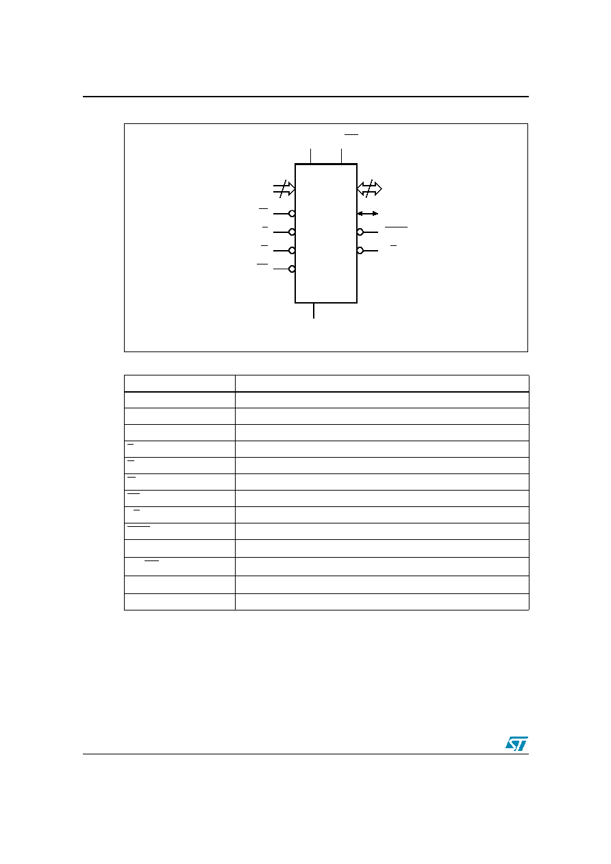
Figure 1.
Logic Diagram
Table 1.
Signal Names
A0-A21
Address Inputs
DQ0-DQ7
Data Inputs/Outputs
DQ8-DQ14
Data Inputs/Outputs
DQ15A
≠
1 (or DQ15)
Data Input/Output or Address Input (or Data Input/Output)
E
Chip Enable
G
Output Enable
W
Write Enable
RP
Reset/Block Temporary Unprotect
RB
Ready/Busy Output
BYTE
Byte/Word Organization Select
V
CC
Supply Voltage
V
PP
/WP
Supply Voltage for Fast Program (optional) or Write Protect
V
SS
Ground
NC
Not Connected Internally
AI11250
22
A0-A21
W
DQ0-DQ14
VCC
M29W640FT
M29W640FB
E
VSS
15
G
RP
DQ15A
≠
1
BYTE
RB
VPP/WP
M29W640FT, M29W640FB
1 Summary description
9/72
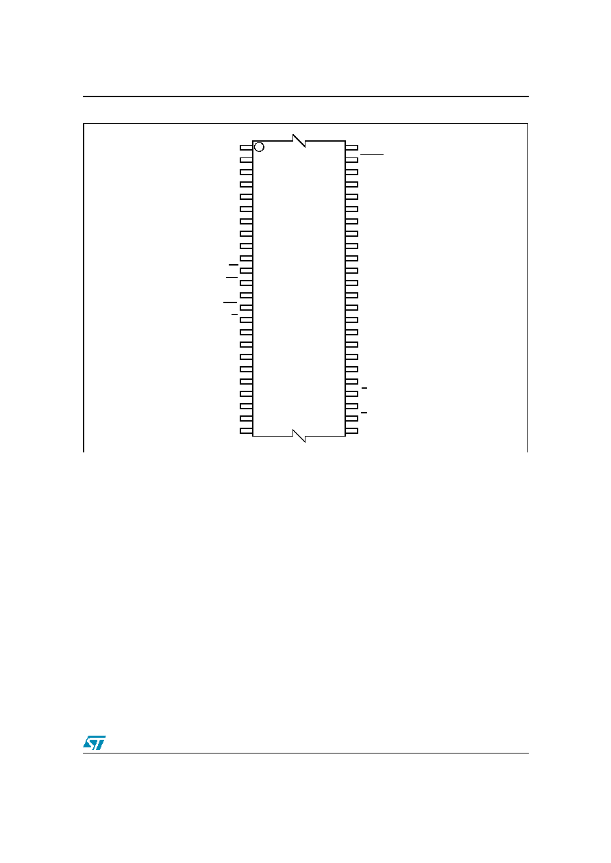
Figure 2.
TSOP Connections
DQ3
DQ9
DQ2
A6
DQ0
W
A3
RB
DQ6
A8
A9
DQ13
A17
A10
DQ14
A2
DQ12
DQ10
DQ15A
≠
1
VCC
DQ4
DQ5
A7
DQ7
VPP/WP
A21
M29W640FT
M29W640FB
12
1
13
24
25
36
37
48
DQ8
A20
A19
A1
A18
A4
A5
DQ1
DQ11
G
A12
A13
A16
A11
BYTE
A15
A14
VSS
E
A0
RP
VSS
AI11251

1 Summary description
M29W640FT, M29W640FB
10/72
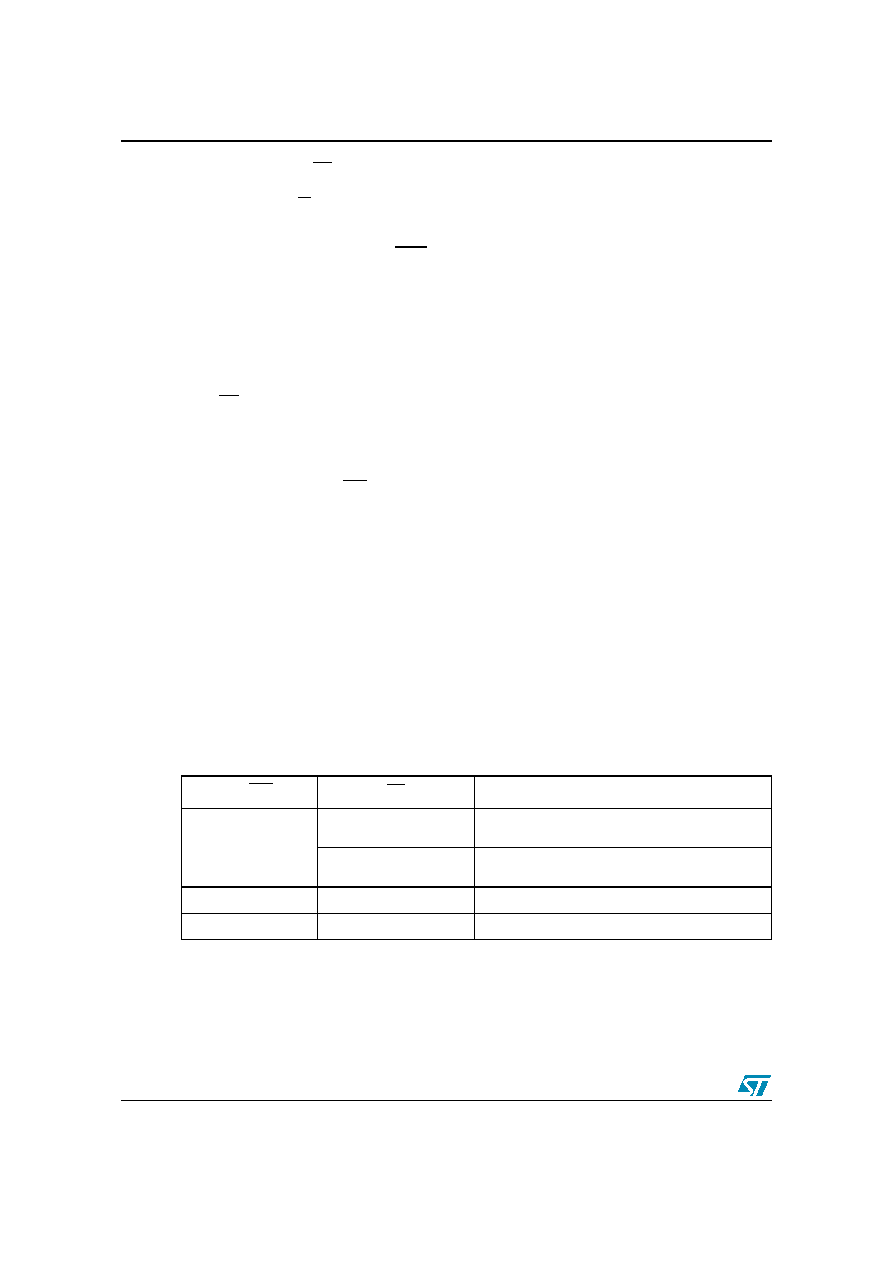
Figure 3.
TFBGA48 Connections (Top view through package)
6
5
4
3
2
1
VSS
A15
A14
A12
A13
DQ3
DQ11
DQ10
A18
VPP
/
WP
RB
DQ1
DQ9
DQ8
DQ0
A6
A17
A7
G
E
A0
A4
A3
DQ2
DQ6
DQ13
DQ14
A10
A8
A9
DQ4
VCC
DQ12
DQ5
A19
A21
RP
W
A11
DQ7
A1
A2
VSS
A5
A20
A16
BYTE
C
B
A
E
D
F
G
H
DQ15
A
≠
1
AI11554

M29W640FT, M29W640FB
2 Signal descriptions
11/72
2
Signal descriptions
See
Figure 1: Logic Diagram
, and
Table 1: Signal Names
, for a brief overview of the signals
connected to this device.
2.1
Address Inputs (A0-A21)
The Address Inputs select the cells in the memory array to access during Bus Read operations.
During Bus Write operations they control the commands sent to the Command Interface of the
Program/Erase Controller.
2.2
Data Inputs/Outputs (DQ0-DQ7)
The Data I/O outputs the data stored at the selected address during a Bus Read operation.
During Bus Write operations they represent the commands sent to the Command Interface of
the Program/Erase Controller.
2.3
Data Inputs/Outputs (DQ8-DQ14)
The Data I/O outputs the data stored at the selected address during a Bus Read operation
when BYTE is High, V
IH
. When BYTE is Low, V
IL
, these pins are not used and are high
impedance. During Bus Write operations the Command Register does not use these bits.
When reading the Status Register these bits should be ignored.
2.4
Data Input/Output or Address Input (DQ15A
≠
1)
When BYTE is High, V
IH
, this pin behaves as a Data Input/Output pin (as DQ8-DQ14). When
BYTE is Low, V
IL
, this pin behaves as an address pin; DQ15A
≠
1 Low will select the LSB of the
addressed Word, DQ15A
≠
1 High will select the MSB. Throughout the text consider references
to the Data Input/Output to include this pin when BYTE is High and references to the Address
Inputs to include this pin when BYTE is Low except when stated explicitly otherwise.
2.5
Chip Enable (E)
The Chip Enable, E, activates the memory, allowing Bus Read and Bus Write operations to be
performed. When Chip Enable is High, V
IH
, all other pins are ignored.
2.6
Output Enable (G)
The Output Enable, G, controls the Bus Read operation of the memory.
2 Signal descriptions
M29W640FT, M29W640FB
12/72
2.7
Write Enable (W)
The Write Enable, W, controls the Bus Write operation of the memory
'
s Command Interface.
2.8
V
PP
/Write Protect (V
PP
/WP)
The V
PP
/Write Protect pin provides two functions. The V
PP
function allows the memory to use
an external high voltage power supply to reduce the time required for Unlock Bypass Program
operations. The Write Protect function provides a hardware method of protecting the two
outermost boot blocks. The V
PP
/Write Protect pin must not be left floating or unconnected.
When V
PP
/Write Protect is Low, V
IL
, the memory protects the two outermost boot blocks;
Program and Erase operations in this block are ignored while V
PP
/Write Protect is Low, even
when RP is at V
ID
.
When V
PP
/Write Protect is High, V
IH
, the memory reverts to the previous protection status of
the two outermost boot blocks. Program and Erase operations can now modify the data in the
two outermost boot blocks unless the block is protected using Block Protection.
Applying V
PPH
to the V
PP
/WP pin will temporarily unprotect any block previously protected
(including the two outermost parameter blocks) using a High Voltage Block Protection
technique (In-System or Programmer technique). See
Table 2: Hardware Protection
for details.
When V
PP
/Write Protect is raised to V
PP
the memory automatically enters the Unlock Bypass
mode. When V
PP
/Write Protect returns to V
IH
or V
IL
normal operation resumes. During Unlock
Bypass Program operations the memory draws I
PP
from the pin to supply the programming
circuits. See the description of the Unlock Bypass command in the Command Interface section.
The transitions from V
IH
to V
PP
and from V
PP
to V
IH
must be slower than t
VHVPP
, see
Figure 13:
Accelerated Program Timing Waveforms
.
Never raise V
PP
/Write Protect to V
PP
from any mode except Read mode, otherwise the
memory may be left in an indeterminate state.
A 0.1
µ
F capacitor should be connected between the V
PP
/Write Protect pin and the V
SS
Ground
pin to decouple the current surges from the power supply. The PCB track widths must be
sufficient to carry the currents required during Unlock Bypass Program, I
PP
.
Table 2.
Hardware Protection
V
PP
/WP
RP
Function
V
IL
V
IH
2 outermost parameter blocks protected from
Program/Erase operations
V
ID
All blocks temporarily unprotected except the 2
outermost blocks
V
IH
or V
ID
V
ID
All blocks temporarily unprotected
V
PPH
V
IH
or V
ID
All blocks temporarily unprotected

M29W640FT, M29W640FB
2 Signal descriptions
13/72
2.9
Reset/Block Temporary Unprotect (RP)
The Reset/Block Temporary Unprotect pin can be used to apply a Hardware Reset to the
memory or to temporarily unprotect all Blocks that have been protected.
Note that if V
PP
/WP is at V
IL
, then the two outermost boot blocks will remain protected even if
RP is at V
ID
.
A Hardware Reset is achieved by holding Reset/Block Temporary Unprotect Low, V
IL
, for at
least t
PLPX
. After Reset/Block Temporary Unprotect goes High, V
IH
, the memory will be ready
for Bus Read and Bus Write operations after t
PHEL
or t
RHEL
, whichever occurs last. See the
Ready/Busy Output section,
Table 16: Reset/Block Temporary Unprotect AC Characteristics
and
Figure 12: Reset/Block Temporary Unprotect AC Waveforms
, for more details.
Holding RP at V
ID
will temporarily unprotect the protected Blocks in the memory. Program and
Erase operations on all blocks will be possible. The transition from V
IH
to V
ID
must be slower
than t
PHPHH
.
2.10 Ready/Busy Output (RB)
The Ready/Busy pin is an open-drain output that can be used to identify when the device is
performing a Program or Erase operation. During Program or Erase operations Ready/Busy is
Low, V
OL
. Ready/Busy is high-impedance during Read mode, Auto Select mode and Erase
Suspend mode.
After a Hardware Reset, Bus Read and Bus Write operations cannot begin until Ready/Busy
becomes high-impedance. See
Table 16: Reset/Block Temporary Unprotect AC Characteristics
and
Figure 12: Reset/Block Temporary Unprotect AC Waveforms
, for more details.
The use of an open-drain output allows the Ready/Busy pins from several memories to be
connected to a single pull-up resistor. A Low will then indicate that one, or more, of the
memories is busy.
2.11 Byte/Word Organization Select (BYTE)
The Byte/Word Organization Select pin is used to switch between the x8 and x16 Bus modes of
the memory. When Byte/Word Organization Select is Low, V
IL
, the memory is in x8 mode, when
it is High, V
IH
, the memory is in x16 mode.
2.12 V
CC
Supply Voltage (2.7V to 3.6V)
V
CC
provides the power supply for all operations (Read, Program and Erase).
The Command Interface is disabled when the V
CC
Supply Voltage is less than the Lockout
Voltage, V
LKO
. This prevents Bus Write operations from accidentally damaging the data during
power up, power down and power surges. If the Program/Erase Controller is programming or
erasing during this time then the operation aborts and the memory contents being altered will
be invalid.
A 0.1
µ
F capacitor should be connected between the V
CC
Supply Voltage pin and the V
SS
Ground pin to decouple the current surges from the power supply. The PCB track widths must
be sufficient to carry the currents required during Program and Erase operations, I
CC3
.

2 Signal descriptions
M29W640FT, M29W640FB
14/72
2.13 V
SS
Ground
V
SS
is the reference for all voltage measurements. The device features two V
SS
pins which
must be both connected to the system ground.

M29W640FT, M29W640FB
3 Bus operations
15/72
3
Bus operations
There are five standard bus operations that control the device. These are Bus Read, Bus Write,
Output Disable, Standby and Automatic Standby. See
Table 3: Bus Operations, BYTE = VIL
and
Table 4: Bus Operations, BYTE = VIH
, for a summary. Typically glitches of less than 5ns on
Chip Enable or Write Enable are ignored by the memory and do not affect bus operations.
3.1
Bus Read
Bus Read operations read from the memory cells, or specific registers in the Command
Interface. A valid Bus Read operation involves setting the desired address on the Address
Inputs, applying a Low signal, V
IL
, to Chip Enable and Output Enable and keeping Write Enable
High, V
IH
. The Data Inputs/Outputs will output the value, see
Figure 8: Read Mode AC
Waveforms
, and
Table 13: Read AC Characteristics
, for details of when the output becomes
valid.
3.2
Bus Write
Bus Write operations write to the Command Interface. To speed up the read operation the
memory array can be read in Page mode where data is internally read and stored in a page
buffer. The Page has a size of 4 Words and is addressed by the address inputs A0-A1.
A valid Bus Write operation begins by setting the desired address on the Address Inputs. The
Address Inputs are latched by the Command Interface on the falling edge of Chip Enable or
Write Enable, whichever occurs last. The Data Inputs/Outputs are latched by the Command
Interface on the rising edge of Chip Enable or Write Enable, whichever occurs first. Output
Enable must remain High, V
IH
, during the whole Bus Write operation. See
Figure 10: Write AC
Waveforms, Write Enable Controlled
,
Figure 11: Write AC Waveforms, Chip Enable Controlled
,
and
Table 14: Write AC Characteristics, Write Enable Controlled
and
Table 15: Write AC
Characteristics, Chip Enable Controlled
, for details of the timing requirements.
3.3
Output Disable
The Data Inputs/Outputs are in the high impedance state when Output Enable is High, V
IH
.
3.4
Standby
When Chip Enable is High, V
IH
, the memory enters Standby mode and the Data Inputs/Outputs
pins are placed in the high-impedance state. To reduce the Supply Current to the Standby
Supply Current, I
CC2
, Chip Enable should be held within V
CC
±
0.2V. For the Standby current
level see
Table 12: DC Characteristics
.
During program or erase operations the memory will continue to use the Program/Erase Supply
Current, I
CC3
, for Program or Erase operations until the operation completes.

3 Bus operations
M29W640FT, M29W640FB
16/72
3.5
Automatic Standby
If CMOS levels (V
CC
±
0.2V) are used to drive the bus and the bus is inactive for 300ns or more
the memory enters Automatic Standby where the internal Supply Current is reduced to the
Standby Supply Current, I
CC2
. The Data Inputs/Outputs will still output data if a Bus Read
operation is in progress.
3.6
Special Bus Operations
Additional bus operations can be performed to read the Electronic Signature and also to apply
and remove Block Protection. These bus operations are intended for use by programming
equipment and are not usually used in applications. They require V
ID
to be applied to some
pins.
3.6.1 Electronic Signature
The memory has two codes, the manufacturer code and the device code, that can be read to
identify the memory. These codes can be read by applying the signals listed in
Table 3: Bus
Operations, BYTE = VIL
and
Table 4: Bus Operations, BYTE = VIH
.
3.6.2 Block Protect and Chip Unprotect
Groups of blocks can be protected against accidental Program or Erase. The Protection
Groups are shown in
Appendix A: Block addresses Table 20
and
Table 21
. The whole chip can
be unprotected to allow the data inside the blocks to be changed.
The V
PP
/Write Protect pin can be used to protect the two outermost boot blocks. When V
PP
/
Write Protect is at V
IL
the two outermost boot blocks are protected and remain protected
regardless of the Block Protection Status or the Reset/Block Temporary Unprotect pin status.
Block Protect and Chip Unprotect operations are described in
Appendix D: Block Protection
.

M29W640FT, M29W640FB
3 Bus operations
17/72
Table 3.
Bus Operations, BYTE = V
IL
1. X = V
IL
or V
IH
.
Operation
E
G
W
Address Inputs
DQ15A
≠
1, A0-A21
Data Inputs/Outputs
DQ14-DQ8
DQ7-DQ0
Bus Read
V
IL
V
IL
V
IH
Cell Address
Hi-Z
Data Output
Bus Write
V
IL
V
IH
V
IL
Command Address
Hi-Z
Data Input
Output Disable
X
V
IH
V
IH
X
Hi-Z
Hi-Z
Standby
V
IH
X
X
X
Hi-Z
Hi-Z
Read Manufacturer
Code
V
IL
V
IL
V
IH
A0-A3 = V
IL
, A6 = V
IL
,
A9 = V
ID
, Others V
IL
or V
IH
Hi-Z
20h
Read Device Code
V
IL
V
IL
V
IH
A0 = V
IH
, A1-A3= V
IL
,
A6 = V
IL
, A9 = V
ID
,
Others V
IL
or V
IH
Hi-Z
EDh (M29W640FT)
FDh (M29W640FB)
Read Extended
Memory Block Verify
Code
V
IL
V
IL
V
IH
A0 -A1 = V
IH
, A2-A3= V
IL
,
A6 = V
IL
, A9 = V
ID
,
Others V
IL
or V
IH
Hi-Z
80h (factory locked)
00h (Customer
Lockable)
Read Block
Protection Status
V
IL
V
IL
V
IH
A0,A2,A3, A6= V
IL
,
A1= V
IH
, A9 = V
ID
,
A12-A21 = Block Address,
Others V
IL
or V
IH
Hi-Z
01h (protected)
00h (unprotected)
3 Bus operations
M29W640FT, M29W640FB
18/72
Table 4.
Bus Operations, BYTE = V
IH
1. X = V
IL
or V
IH
.
Operation
E
G
W
Address Inputs
A0-A21
Data Inputs/Outputs
DQ15A
≠
1, DQ14-DQ0
Bus Read
V
IL
V
IL
V
IH
Cell Address
Data Output
Bus Write
V
IL
V
IH
V
IL
Command Address
Data Input
Output Disable
X
V
IH
V
IH
X
Hi-Z
Standby
V
IH
X
X
X
Hi-Z
Read Manufacturer
Code
V
IL
V
IL
V
IH
A0-A3 = V
IL
, A6 = V
IL
,
A9 = V
ID
, Others V
IL
or V
IH
0020h
Read Device Code
V
IL
V
IL
V
IH
A0 = V
IH
, A1-A3= V
IL
, A6 = V
IL
,
A9 = V
ID
, Others V
IL
or V
IH
22EDh (M29W640FT)
22FDh (M29W640FB)
Read Extended
Memory Block Verify
Code
V
IL
V
IL
V
IH
A0 -A1 = V
IH
, A2-A3= V
IL
,
A6 = V
IL
, A9 = V
ID
,
Others V
IL
or V
IH
80h (factory locked)
00h (Customer Lockable)
Read Block
Protection Status
V
IL
V
IL
V
IH
A0,A2,A3, A6= V
IL
,
A1 = V
IH
, A9 = V
ID
,
A12-A21 = Block Address,
Others V
IL
or V
IH
0001h (protected)
0000h (unprotected)

M29W640FT, M29W640FB
4 Command Interface
19/72
4
Command Interface
All Bus Write operations to the memory are interpreted by the Command Interface. Commands
consist of one or more sequential Bus Write operations. Failure to observe a valid sequence of
Bus Write operations will result in the memory returning to Read mode. The long command
sequences are imposed to maximize data security.
The address used for the commands changes depending on whether the memory is in 16-bit or
8-bit mode. See either
Table 5
, or
Table 6
, depending on the configuration that is being used,
for a summary of the commands.
4.1
Standard commands
4.1.1 Read/Reset command
The Read/Reset command returns the memory to its Read mode. It also resets the errors in
the Status Register. Either one or three Bus Write operations can be used to issue the Read/
Reset command.
The Read/Reset command can be issued, between Bus Write cycles before the start of a
program or erase operation, to return the device to read mode. If the Read/Reset command is
issued during the timeout of a Block Erase operation then the memory will take up to 10
µ
s to
abort. During the abort period no valid data can be read from the memory. The Read/Reset
command will not abort an Erase operation when issued while in Erase Suspend.
4.1.2 Auto Select command
The Auto Select command is used to read the Manufacturer Code, the Device Code, the Block
Protection Status and the Extended Memory Block Verify Code. Three consecutive Bus Write
operations are required to issue the Auto Select command. Once the Auto Select command is
issued the memory remains in Auto Select mode until a Read/Reset command is issued. Read
CFI Query and Read/Reset commands are accepted in Auto Select mode, all other commands
are ignored.
In Auto Select mode, the Manufacturer Code and the Device Code can be read by using a Bus
Read operation with addresses and control signals set as shown in
Table 3: Bus Operations,
BYTE = VIL
and
Table 4: Bus Operations, BYTE = VIH
, except for A9 that is
`
Don
'
t Care
'
.
The Block Protection Status of each block can be read using a Bus Read operation with
addresses and control signals set as shown in
Table 3: Bus Operations, BYTE = VIL
and
Table 4: Bus Operations, BYTE = VIH
, except for A9 that is
`
Don
'
t Care
'
. If the addressed block
is protected then 01h is output on Data Inputs/Outputs DQ0-DQ7, otherwise 00h is output (in
8-bit mode).
The protection status of the Extended Memory block, or Extended Memory Block Verify code,
can be read using a Bus Read operation with addresses and control signals set as shown in
Table 3: Bus Operations, BYTE = VIL
and
Table 4: Bus Operations, BYTE = VIH
, except for A9
that is
`
Don
'
t Care
'
. If the Extended Block is "Factory Locked" then 80h is output on Data Input/
Outputs DQ0-DQ7, otherwise 00h is output (8-bit mode).

4 Command Interface
M29W640FT, M29W640FB
20/72
4.1.3 Read CFI Query command
The Read CFI Query Command is used to read data from the Common Flash Interface (CFI)
Memory Area. This command is valid when the device is in the Read Array mode, or when the
device is in Autoselected mode.
One Bus Write cycle is required to issue the Read CFI Query Command. Once the command is
issued subsequent Bus Read operations read from the Common Flash Interface Memory Area.
The Read/Reset command must be issued to return the device to the previous mode (the Read
Array mode or Autoselected mode). A second Read/Reset command would be needed if the
device is to be put in the Read Array mode from Autoselected mode.
See
Appendix B: Common Flash Interface (CFI)
, Tables
22
,
23
,
24
,
25
,
26
and
27
for details on
the information contained in the Common Flash Interface (CFI) memory area.
4.1.4 Chip Erase command
The Chip Erase command can be used to erase the entire chip. Six Bus Write operations are
required to issue the Chip Erase Command and start the Program/Erase Controller.
If any blocks are protected then these are ignored and all the other blocks are erased. If all of
the blocks are protected the Chip Erase operation appears to start but will terminate within
about 100
µ
s, leaving the data unchanged. No error condition is given when protected blocks
are ignored.
During the erase operation the memory will ignore all commands, including the Erase Suspend
command. It is not possible to issue any command to abort the operation. Typical chip erase
times are given in
Table 7: Program, Erase Times and Program, Erase Endurance Cycles
. All
Bus Read operations during the Chip Erase operation will output the Status Register on the
Data Inputs/Outputs. See the section on the Status Register for more details.
After the Chip Erase operation has completed the memory will return to the Read Mode, unless
an error has occurred. When an error occurs the memory will continue to output the Status
Register. A Read/Reset command must be issued to reset the error condition and return to
Read Mode.
The Chip Erase Command sets all of the bits in unprotected blocks of the memory to
'
1
'
. All
previous data is lost.
4.1.5 Block Erase command
The Block Erase command can be used to erase a list of one or more blocks. Six Bus Write
operations are required to select the first block in the list. Each additional block in the list can be
selected by repeating the sixth Bus Write operation using the address of the additional block.
The Block Erase operation starts the Program/Erase Controller about 50
µ
s after the last Bus
Write operation. Once the Program/Erase Controller starts it is not possible to select any more
blocks. Each additional block must therefore be selected within 50
µ
s of the last block. The 50
µ
s
timer restarts when an additional block is selected. The Status Register can be read after the
sixth Bus Write operation. See the Status Register section for details on how to identify if the
Program/Erase Controller has started the Block Erase operation.
If any selected blocks are protected then these are ignored and all the other selected blocks are
erased. If all of the selected blocks are protected the Block Erase operation appears to start but
will terminate within about 100
µ
s, leaving the data unchanged. No error condition is given when
protected blocks are ignored.

M29W640FT, M29W640FB
4 Command Interface
21/72
During the Block Erase operation the memory will ignore all commands except the Erase
Suspend command. Typical block erase times are given in
Table 7: Program, Erase Times and
Program, Erase Endurance Cycles
. All Bus Read operations during the Block Erase operation
will output the Status Register on the Data Inputs/Outputs. See the section on the Status
Register for more details.
After the Block Erase operation has completed the memory will return to the Read Mode,
unless an error has occurred. When an error occurs the memory will continue to output the
Status Register. A Read/Reset command must be issued to reset the error condition and return
to Read mode.
The Block Erase Command sets all of the bits in the unprotected selected blocks to
'
1
'
. All
previous data in the selected blocks is lost.
4.1.6 Erase Suspend command
The Erase Suspend Command may be used to temporarily suspend a Block Erase operation
and return the memory to Read mode. The command requires one Bus Write operation.
The Program/Erase Controller will suspend within the Erase Suspend Latency time of the
Erase Suspend Command being issued. Once the Program/Erase Controller has stopped the
memory will be set to Read mode and the Erase will be suspended. If the Erase Suspend
command is issued during the period when the memory is waiting for an additional block
(before the Program/Erase Controller starts) then the Erase is suspended immediately and will
start immediately when the Erase Resume Command is issued. It is not possible to select any
further blocks to erase after the Erase Resume.
During Erase Suspend it is possible to Read and Program cells in blocks that are not being
erased; both Read and Program operations behave as normal on these blocks. If any attempt is
made to program in a protected block or in the suspended block then the Program command is
ignored and the data remains unchanged. The Status Register is not read and no error
condition is given. Reading from blocks that are being erased will output the Status Register.
It is also possible to issue the Auto Select, Read CFI Query and Unlock Bypass commands
during an Erase Suspend. The Read/Reset command must be issued to return the device to
Read Array mode before the Resume command will be accepted.
4.1.7 Erase Resume command
The Erase Resume command must be used to restart the Program/Erase Controller after an
Erase Suspend. The device must be in Read Array mode before the Resume command will be
accepted. An erase can be suspended and resumed more than once.
4.1.8 Program Suspend command
The Program Suspend command allows the system to interrupt a program operation so that
data can be read from any block. When the Program Suspend command is issued during a
program operation, the device suspends the program operation within the Program Suspend
Latency time (see
Table 7: Program, Erase Times and Program, Erase Endurance Cycles
for
value) and updates the Status Register bits.
After the program operation has been suspended, the system can read array data from any
address. However, data read from Program-Suspended addresses is not valid.
The Program Suspend command may also be issued during a program operation while an
erase is suspended. In this case, data may be read from any addresses not in Erase Suspend

4 Command Interface
M29W640FT, M29W640FB
22/72
or Program Suspend. If a read is needed from the Extended Block area (One-time Program
area), the user must use the proper command sequences to enter and exit this region.
The system may also issue the Auto Select command sequence when the device is in the
Program Suspend mode. The system can read as many Auto Select codes as required. When
the device exits the Auto Select mode, the device reverts to the Program Suspend mode, and is
ready for another valid operation. See Auto Select command sequence for more information.
4.1.9 Program Resume command
After the Program Resume command is issued, the device reverts to programming. The
controller can determine the status of the program operation using the DQ7 or DQ6 status bits,
just as in the standard program operation. See Write Operation Status for more information.
The system must write the Program Resume command, to exit the Program Suspend mode
and to continue the programming operation.
Further issuing of the Resume command is ignored. Another Program Suspend command can
be written after the device has resumed programming.
4.1.10 Program command
The Program command can be used to program a value to one address in the memory array at
a time. The command requires four Bus Write operations, the final write operation latches the
address and data, and starts the Program/Erase Controller.
Programming can be suspended and then resumed by issuing a Program Suspend command
and a Program Resume command, respectively (see
Section 4.1.8: Program Suspend
command
and
Section 4.1.9: Program Resume command
).
If the address falls in a protected block then the Program command is ignored, the data remains
unchanged. The Status Register is never read and no error condition is given.
During the program operation the memory will ignore all commands. It is not possible to issue
any command to abort or pause the operation. Typical program times are given in
Table 7:
Program, Erase Times and Program, Erase Endurance Cycles
. Bus Read operations during
the program operation will output the Status Register on the Data Inputs/Outputs. See the
section on the Status Register for more details.
After the program operation has completed the memory will return to the Read mode, unless an
error has occurred. When an error occurs the memory will continue to output the Status
Register. A Read/Reset command must be issued to reset the error condition and return to
Read mode.
Note that the Program command cannot change a bit set at
'
0
'
back to
'
1
'
. One of the Erase
Commands must be used to set all the bits in a block or in the whole memory from
'
0
'
to
'
1
'
.

M29W640FT, M29W640FB
4 Command Interface
23/72
4.2
Fast Program commands
There are four Fast Program commands available to improve the programming throughput, by
writing several adjacent words or bytes in parallel. The Double, Quadruple and Octuple Byte
Program commands are available for x8 operations, while the Double Quadruple Word Program
command are available for x16 operations.
Fast Program commands can be suspended and then resumed by issuing a Program Suspend
command and a Program Resume command, respectively (see
Section 4.1.8: Program
Suspend command
and
Section 4.1.9: Program Resume command
).
When V
PPH
is applied to the V
PP
/Write Protect pin the memory automatically enters the Fast
Program mode. The user can then choose to issue any of the Fast Program commands. Care
must be taken because applying a V
PPH
to the V
PP
/WP pin will temporarily unprotect any
protected block.
4.2.1 Double Byte Program command
The Double Byte Program command is used to write a page of two adjacent Bytes in parallel.
The two bytes must differ only in DQ15A-1. Three bus write cycles are necessary to issue the
Double Byte Program command.
1.
The first bus cycle sets up the Double Byte Program Command.
2. The second bus cycle latches the Address and the Data of the first byte to be written.
3. The third bus cycle latches the Address and the Data of the second byte to be written.
4.2.2 Quadruple Byte Program command
The Quadruple Byte Program command is used to write a page of four adjacent Bytes in
parallel. The four bytes must differ only for addresses A0, DQ15A-1. Five bus write cycles are
necessary to issue the Quadruple Byte Program command.
1.
The first bus cycle sets up the Quadruple Byte Program Command.
2. The second bus cycle latches the Address and the Data of the first byte to be written.
3. The third bus cycle latches the Address and the Data of the second byte to be written.
4. The fourth bus cycle latches the Address and the Data of the third byte to be written.
5. The fifth bus cycle latches the Address and the Data of the fourth byte to be written and
starts the Program/Erase Controller.

4 Command Interface
M29W640FT, M29W640FB
24/72
4.2.3 Octuple Byte Program command
This is used to write eight adjacent Bytes, in x8 mode, simultaneously. The addresses of the
eight Bytes must differ only in A1, A0 and DQ15A-1.
Nine bus write cycles are necessary to issue the command:
1.
The first bus cycle sets up the command.
2. The second bus cycle latches the Address and the Data of the first Byte to be written.
3. The third bus cycle latches the Address and the Data of the second Byte to be written.
4. The fourth bus cycle latches the Address and the Data of the third Byte to be written.
5. The fifth bus cycle latches the Address and the Data of the fourth Byte to be written.
6. The sixth bus cycle latches the Address and the Data of the fifth Byte to be written.
7. The seventh bus cycle latches the Address and the Data of the sixth Byte to be written.
8. The eighth bus cycle latches the Address and the Data of the seventh Byte to be written.
9. The ninth bus cycle latches the Address and the Data of the eighth Byte to be written and
starts the Program/Erase Controller.
4.2.4 Double Word Program command
The Double Word Program command is used to write a page of two adjacent Words in parallel.
The two Words must differ only for the address A0.
Three bus write cycles are necessary to issue the Double Word Program command.
The first bus cycle sets up the Quadruple Word Program Command.
The second bus cycle latches the Address and the Data of the first Word to be written.
The third bus cycle latches the Address and the Data of the second Word to be written and
starts the Program/Erase Controller.
After the program operation has completed the memory will return to the Read mode, unless an
error has occurred. When an error occurs Bus Read operations will continue to output the
Status Register. A Read/Reset command must be issued to reset the error condition and return
to Read mode.
Note that the Fast Program commands cannot change a bit set at
'
0
'
back to
'
1
'
. One of the
Erase Commands must be used to set all the bits in a block or in the whole memory from
'
0
'
to
'
1
'
.
Typical Program times are given in
Table 7: Program, Erase Times and Program, Erase
Endurance Cycles
.

M29W640FT, M29W640FB
4 Command Interface
25/72
4.2.5 Quadruple Word Program command
This is used to write a page of four adjacent Words (or 8 adjacent Bytes), in x16 mode,
simultaneously. The addresses of the four Words must differ only in A1 and A0.
Five bus write cycles are necessary to issue the command:
The first bus cycle sets up the command.
The second bus cycle latches the Address and the Data of the first Word to be written.
The third bus cycle latches the Address and the Data of the second Word to be written.
The fourth bus cycle latches the Address and the Data of the third Word to be written.
The fifth bus cycle latches the Address and the Data of the fourth Word to be written and
starts the Program/Erase Controller.
4.2.6 Unlock Bypass command
The Unlock Bypass command is used in conjunction with the Unlock Bypass Program
command to program the memory faster than with the standard program commands. When the
cycle time to the device is long, considerable time saving can be made by using these
commands. Three Bus Write operations are required to issue the Unlock Bypass command.
Once the Unlock Bypass command has been issued the memory will only accept the Unlock
Bypass Program command and the Unlock Bypass Reset command. The memory can be read
as if in Read mode.
When V
PP
is applied to the V
PP
/Write Protect pin the memory automatically enters the Unlock
Bypass mode and the Unlock Bypass Program command can be issued immediately.
4.2.7 Unlock Bypass Program command
The Unlock Bypass command is used in conjunction with the Unlock Bypass Program
command to program the memory. When the cycle time to the device is long, considerable time
saving can be made by using these commands. Three Bus Write operations are required to
issue the Unlock Bypass command.
Once the Unlock Bypass command has been issued the memory will only accept the Unlock
Bypass Program command and the Unlock Bypass Reset command. The memory can be read
as if in Read mode.
The memory offers accelerated program operations through the V
PP
/Write Protect pin. When
the system asserts V
PP
on the V
PP
/Write Protect pin, the memory automatically enters the
Unlock Bypass mode. The system may then write the two-cycle Unlock Bypass program
command sequence. The memory uses the higher voltage on the V
PP
/Write Protect pin, to
accelerate the Unlock Bypass Program operation.
Never raise V
PP
/Write Protect to V
PP
from any mode except Read mode, otherwise the
memory may be left in an indeterminate state.
4.2.8 Unlock Bypass Reset command
The Unlock Bypass Reset command can be used to return to Read/Reset mode from Unlock
Bypass Mode. Two Bus Write operations are required to issue the Unlock Bypass Reset
command. Read/Reset command does not exit from Unlock Bypass Mode.

4 Command Interface
M29W640FT, M29W640FB
26/72
4.3
Block Protection commands
4.3.1 Enter Extended Block command
The device has an extra 256 Byte block (Extended Block) that can only be accessed using the
Enter Extended Block command. Three Bus write cycles are required to issue the Extended
Block command. Once the command has been issued the device enters Extended Block mode
where all Bus Read or Write operations to the Boot Block addresses access the Extended
Block. The Extended Block (with the same address as the Boot Blocks) cannot be erased, and
can be treated as one-time programmable (OTP) memory. In Extended Block mode the Boot
Blocks are not accessible.
To exit from the Extended Block mode the Exit Extended Block command must be issued.
The Extended Block can be protected, however once protected the protection cannot be
undone.
4.3.2 Exit Extended Block command
The Exit Extended Block command is used to exit from the Extended Block mode and return
the device to Read mode. Four Bus Write operations are required to issue the command.
M29W640FT, M29W640FB
4 Command Interface
27/72
4.3.3 Block Protect and Chip Unprotect commands
Groups of blocks can be protected against accidental Program or Erase. The Protection
Groups are shown in
Appendix A: Block addresses
,
Table 20: Top Boot Block Addresses,
M29W640FT
and
Table 21: Bottom Boot Block Addresses, M29W640FB
. The whole chip can
be unprotected to allow the data inside the blocks to be changed.
Block Protect and Chip Unprotect operations are described in
Appendix D: Block Protection
.
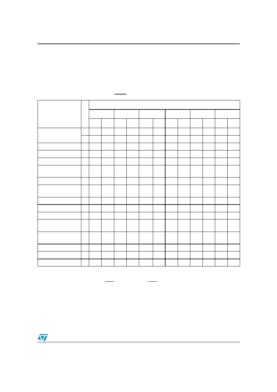
Table 5.
Commands, 16-bit mode, BYTE = V
IH
1. X Don
'
t Care, PA Program Address, PD Program Data, BA Any address in the Block. All values in the table are in
hexadecimal.
The Command Interface only uses A
≠
1, A0-A10 and DQ0-DQ7 to verify the commands; A11-A20, DQ8-DQ14 and DQ15
are Don
'
t Care. DQ15A
≠
1 is A
≠
1 when BYTE is V
IL
or DQ15 when BYTE is V
IH
.
Command
L
e
n
g
t
h
Bus Write Operations
1st
2nd
3rd
4th
5th
6th
Addr Data Addr Data Addr Data Addr Data Addr Data Addr Data
Read/Reset
1
X
F0
3
555
AA
2AA
55
X
F0
Auto Select
3
555
AA
2AA
55
555
90
Program
4
555
AA
2AA
55
555
A0
PA
PD
Double Word Program
3
555
50
PA0
PD0
PA1
PD1
Quadruple Word
Program
5
555
56
PA0
PD0
PA1
PD1
PA2
PD2
PA3
PD3
Unlock Bypass
3
555
AA
2AA
55
555
20
Unlock Bypass
Program
2
X
A0
PA
PD
Unlock Bypass Reset
2
X
90
X
00
Chip Erase
6
555
AA
2AA
55
555
80
555
AA
2AA
55
555
10
Block Erase
6+
555
AA
2AA
55
555
80
555
AA
2AA
55
BA
30
Program/Erase
Suspend
1
X
B0
Program/Erase
Resume
1
X
30
Read CFI Query
1
55
98
Enter Extended Block
3
555
AA
2AA
55
555
88
Exit Extended Block
4
555
AA
2AA
55
555
90
X
00

4 Command Interface
M29W640FT, M29W640FB
28/72
Table 6.
Commands, 8-bit mode, BYTE = V
IL
1. X Don
'
t Care, PA Program Address, PD Program Data, BA Any address in the Block. All values in the table are in
hexadecimal.
The Command Interface only uses A
≠
1, A0-A10 and DQ0-DQ7 to verify the commands; A11-A20, DQ8-DQ14 and DQ15
are Don
'
t Care. DQ15A
≠
1 is A
≠
1 when BYTE is V
IL
or DQ15 when BYTE is V
IH
.
Command
L
e
n
g
t
h
Bus Write Operations
1st
2nd
3rd
4th
5th
6th
7th
8th
9th
Add
Data
Add Data
Add
Data Add
Data Add
Data Add
Data Add
Data Add
Data Add
Data
Read/Reset
1
X
F0
3
AAA
AA
555
55
X
F0
Auto Select
3
AAA
AA
555
55
AAA
90
Program
4
AAA
AA
555
55
AAA
A0
PA
PD
Double Byte
Program
3
AAA
50
PA0
PD0
PA1
PD1
PA2
PD2
Quadruple
Byte Program
5
AAA
56
PA0
PD0
PA1
PD1
PA2
PD2
PA3
PD3
Octuple Byte
Program
9
AAA
8B
PA0
PD0
PA1
PD1
PA2
PD2
PA3
PD3
PA4
PD4
PA5
PD5
PA6
PD6
PA7
PD7
Unlock
Bypass
3
AAA
AA
555
55
AAA
20
Unlock
Bypass
Program
2
X
A0
PA
PD
Unlock
Bypass Reset
2
X
90
X
00
Chip Erase
6
AAA
AA
555
55
AAA
80
AAA
AA
555
55
AAA
10
Block Erase
6
+
AAA
AA
555
55
AAA
80
AAA
AA
555
55
BA
30
Program/
Erase
Suspend
1
X
B0
Program/
Erase
Resume
1
X
30
Read CFI
Query
1
AA
98
Enter
Extended
Block
3
AAA
AA
555
55
AAA
88
Exit Extended
Block
4
AAA
AA
555
55
AAA
90
X
00

M29W640FT, M29W640FB
4 Command Interface
29/72
Table 7.
Program, Erase Times and Program, Erase Endurance Cycles
Parameter
Min
Typ
(1) (2)
1. Typical values measured at room temperature and nominal voltages.
2. Sampled, but not 100% tested.
Max
(2)
Unit
Chip Erase
80
400
(3)
3. Maximum value measured at worst case conditions for both temperature and V
CC
after 100,00 program/erase cycles.
s
Block Erase (64 KBytes)
0.8
6
(4)
s
Erase Suspend Latency Time
50
(4)
4. Maximum value measured at worst case conditions for both temperature and V
CC
.
µ
s
Program (Byte or Word)
10
200
(3)
µ
s
Double Byte
10
200
(3)
µ
s
Double Word /Quadruple Byte Program
10
200
(3)
µ
s
Quadruple Word / Octuple Byte Program
10
200
(3)
µ
s
Chip Program (Byte by Byte)
80
400
(3)
s
Chip Program (Word by Word)
40
200
(3)
s
Chip Program (Double Word/Quadruple Byte Program)
20
100
(3)
s
Chip Program (Quadruple Word/Octuple Byte Program)
10
50
(3)
s
Program Suspend Latency Time
4
µ
s
Program/Erase Cycles (per Block)
100,000
cycles
Data Retention
20
years

5 Status Register
M29W640FT, M29W640FB
30/72
5
Status Register
Bus Read operations from any address always read the Status Register during Program and
Erase operations. It is also read during Erase Suspend when an address within a block being
erased is accessed.
The bits in the Status Register are summarized in
Table 8: Status Register Bits
.
5.1
Data Polling Bit (DQ7)
The Data Polling Bit can be used to identify whether the Program/Erase Controller has
successfully completed its operation or if it has responded to an Erase Suspend. The Data
Polling Bit is output on DQ7 when the Status Register is read.
During Program operations the Data Polling Bit outputs the complement of the bit being
programmed to DQ7. After successful completion of the Program operation the memory returns
to Read mode and Bus Read operations from the address just programmed output DQ7, not its
complement.
During Erase operations the Data Polling Bit outputs
'
0
'
, the complement of the erased state of
DQ7. After successful completion of the Erase operation the memory returns to Read Mode.
In Erase Suspend mode the Data Polling Bit will output a
'
1
'
during a Bus Read operation within
a block being erased. The Data Polling Bit will change from a
'
0
'
to a
'
1
'
when the Program/
Erase Controller has suspended the Erase operation.
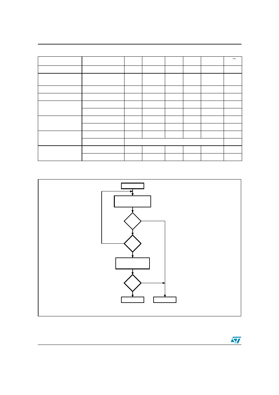
Figure 4: Data Polling Flowchart
, gives an example of how to use the Data Polling Bit. A Valid
Address is the address being programmed or an address within the block being erased.
5.2
Toggle Bit (DQ6)
The Toggle Bit can be used to identify whether the Program/Erase Controller has successfully
completed its operation or if it has responded to an Erase Suspend. The Toggle Bit is output on
DQ6 when the Status Register is read.
During Program and Erase operations the Toggle Bit changes from
'
0
'
to
'
1
'
to
'
0
'
, etc., with
successive Bus Read operations at any address. After successful completion of the operation
the memory returns to Read mode.
During Erase Suspend mode the Toggle Bit will output when addressing a cell within a block
being erased. The Toggle Bit will stop toggling when the Program/Erase Controller has
suspended the Erase operation.
Figure 5: Data Toggle Flowchart
, gives an example of how to use the Data Toggle Bit.

M29W640FT, M29W640FB
5 Status Register
31/72
5.3
Error Bit (DQ5)
The Error Bit can be used to identify errors detected by the Program/Erase Controller. The Error
Bit is set to
'
1
'
when a Program, Block Erase or Chip Erase operation fails to write the correct
data to the memory. If the Error Bit is set a Read/Reset command must be issued before other
commands are issued. The Error bit is output on DQ5 when the Status Register is read.
Note that the Program command cannot change a bit set to
'
0
'
back to
'
1
'
and attempting to do
so will set DQ5 to
`
1
'
. A Bus Read operation to that address will show the bit is still
`
0
'
. One of
the Erase commands must be used to set all the bits in a block or in the whole memory from
'
0
'
to
'
1
'
.
5.4
Erase Timer Bit (DQ3)
The Erase Timer Bit can be used to identify the start of Program/Erase Controller operation
during a Block Erase command. Once the Program/Erase Controller starts erasing the Erase
Timer Bit is set to
'
1
'
. Before the Program/Erase Controller starts the Erase Timer Bit is set to
'
0
'
and additional blocks to be erased may be written to the Command Interface. The Erase Timer
Bit is output on DQ3 when the Status Register is read.
5.5
Alternative Toggle Bit (DQ2)
The Alternative Toggle Bit can be used to monitor the Program/Erase controller during Erase
operations. The Alternative Toggle Bit is output on DQ2 when the Status Register is read.
During Chip Erase and Block Erase operations the Toggle Bit changes from
'
0
'
to
'
1
'
to
'
0
'
, etc.,
with successive Bus Read operations from addresses within the blocks being erased. A
protected block is treated the same as a block not being erased. Once the operation completes
the memory returns to Read mode.
During Erase Suspend the Alternative Toggle Bit changes from
'
0
'
to
'
1
'
to
'
0
'
, etc. with
successive Bus Read operations from addresses within the blocks being erased. Bus Read
operations to addresses within blocks not being erased will output the memory cell data as if in
Read mode.
After an Erase operation that causes the Error Bit to be set the Alternative Toggle Bit can be
used to identify which block or blocks have caused the error. The Alternative Toggle Bit
changes from
'
0
'
to
'
1
'
to
'
0
'
, etc. with successive Bus Read Operations from addresses within
blocks that have not erased correctly. The Alternative Toggle Bit does not change if the
addressed block has erased correctly.
5 Status Register
M29W640FT, M29W640FB
32/72
Table 8.
Status Register Bits
1. Unspecified data bits should be ignored.
Figure 4.
Data Polling Flowchart
Operation
Address
DQ7
DQ6
DQ5
DQ3
DQ2
RB
Program
Any Address
DQ7
Toggle
0
≠
≠
0
Program During Erase
Suspend
Any Address
DQ7
Toggle
0
≠
≠
0
Program Error
Any Address
DQ7
Toggle
1
≠
≠
Hi-Z
Chip Erase
Any Address
0
Toggle
0
1
Toggle
Hi-Z
Block Erase before
timeout
Erasing Block
0
Toggle
0
0
Toggle
0
Non-Erasing Block
0
Toggle
0
0
No Toggle
0
Block Erase
Erasing Block
0
Toggle
0
1
Toggle
Hi-Z
Non-Erasing Block
0
Toggle
0
1
No Toggle
0
Erase Suspend
Erasing Block
1
No Toggle
0
≠
Toggle
Hi-Z
Non-Erasing Block
Data read as normal
Hi-Z
Erase Error
Good Block Address
0
Toggle
1
1
No Toggle
0
Faulty Block Address
0
Toggle
1
1
Toggle
0
READ DQ5 & DQ7
at VALID ADDRESS
START
READ DQ7
at VALID ADDRESS
FAIL
PASS
AI90194
DQ7
=
DATA
YES
NO
YES
NO
DQ5
= 1
DQ7
=
DATA
YES
NO

M29W640FT, M29W640FB
5 Status Register
33/72
Figure 5.
Data Toggle Flowchart
READ DQ6
START
READ DQ6
TWICE
FAIL
PASS
AI90195B
DQ6
=
TOGGLE
NO
NO
YES
YES
DQ5
= 1
NO
YES
DQ6
=
TOGGLE
READ
DQ5 & DQ6
6 Maximum rating
M29W640FT, M29W640FB
34/72
6
Maximum rating
Stressing the device above the rating listed in the Absolute Maximum Ratings table may cause
permanent damage to the device. Exposure to Absolute Maximum Rating conditions for
extended periods may affect device reliability. These are stress ratings only and operation of
the device at these or any other conditions above those indicated in the Operating sections of
this specification is not implied. Refer also to the STMicroelectronics SURE Program and other
relevant quality documents.
Table 9.
Absolute Maximum Ratings
Symbol
Parameter
Min
Max
Unit
T
BIAS
Temperature Under Bias
≠
50
125
∞
C
T
STG
Storage Temperature
≠
65
150
∞
C
V
IO
Input or Output Voltage
(1)(2)
1. Minimum voltage may undershoot to
≠
2V during transition and for less than 20ns during transitions.
2. Maximum voltage may overshoot to V
CC
+2V during transition and for less than 20ns during transitions.
≠
0.6
V
CC
+0.6
V
V
CC
Supply Voltage
≠
0.6
4
V
V
ID
Identification Voltage
≠
0.6
13.5
V
V
PP
(3)
3. V
PP
must not remain at 12V for more than a total of 80hrs.
Program Voltage
≠
0.6
13.5
V
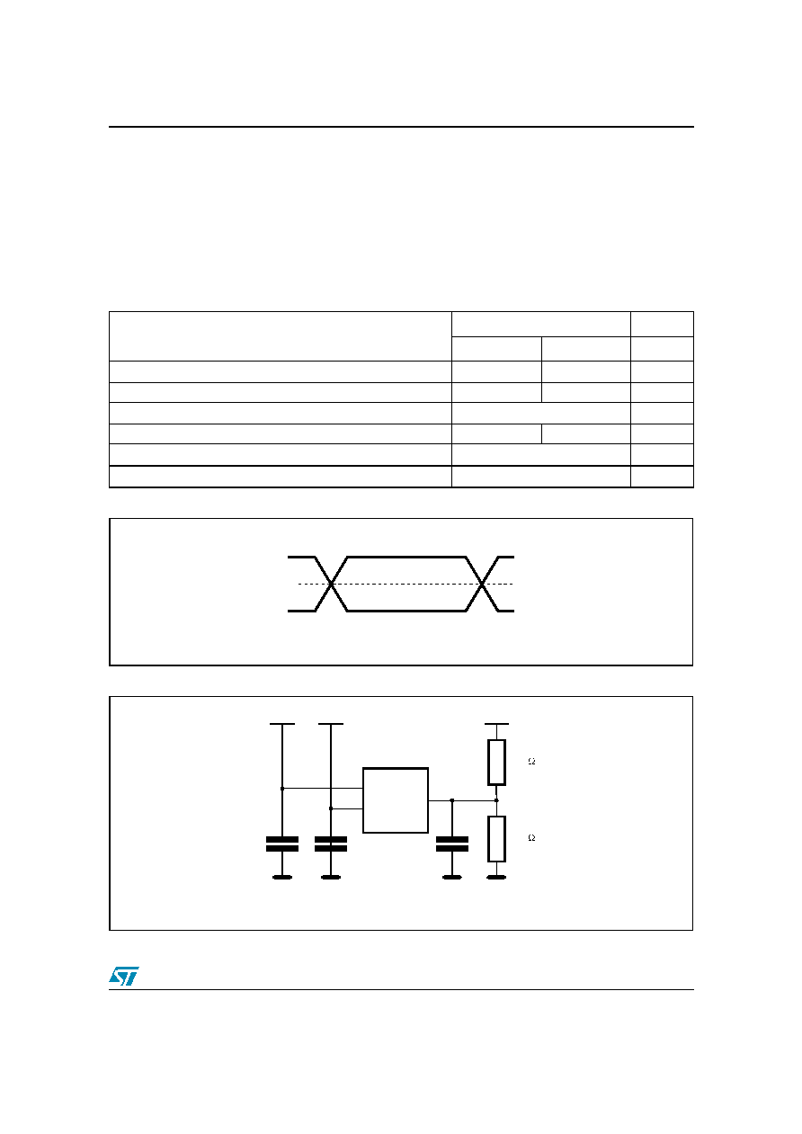
M29W640FT, M29W640FB
7 DC and AC parameters
35/72
7
DC and AC parameters
This section summarizes the operating and measurement conditions, and the DC and AC
characteristics of the device. The parameters in the DC and AC Characteristic tables that follow
are derived from tests performed under the Measurement Conditions summarized in the
relevant tables. Designers should check that the operating conditions in their circuit match the
measurement conditions when relying on the quoted parameters.
Table 10.
Operating and AC Measurement Conditions
Figure 6.
AC Measurement I/O Waveform
Figure 7.
AC Measurement Load Circuit
Parameter
M29W640FT, M29W640FB
Unit
Min
Max
V
CC
Supply Voltage
2.7
3.6
V
Ambient Operating Temperature
≠
40
85
∞
C
Load Capacitance (C
L
)
30
pF
Input Rise and Fall Times
10
ns
Input Pulse Voltages
0 to V
CC
V
Input and Output Timing Ref. Voltages
V
CC
/2
V
AI05557
VCC
0V
VCC/2
AI05558
CL
CL includes JIG capacitance
DEVICE
UNDER
TEST
25k
VCC
25k
VCC
0.1
µ
F
VPP
0.1
µ
F
7 DC and AC parameters
M29W640FT, M29W640FB
36/72
Table 11.
Device Capacitance
1. Sampled only, not 100% tested.
Table 12.
DC Characteristics
Symbol
Parameter
Test Condition
Min
Max
Unit
C
IN
Input Capacitance
V
IN
= 0V
6
pF
C
OUT
Output Capacitance
V
OUT
= 0V
12
pF
Symbol
Parameter
Test Condition
Min
Max
Unit
I
LI
Input Leakage Current
0V V
IN
V
CC
±
1
µ
A
I
LO
Output Leakage Current
0V V
OUT
V
CC
±
1
µ
A
I
CC1
Supply Current (Read)
E = V
IL
, G = V
IH
,
f = 6MHz
10
mA
I
CC2
Supply Current (Standby)
E = V
CC
±
0.2V,
RP = V
CC
±
0.2V
100
µ
A
I
CC3
Supply Current (Program/
Erase)
Program/Erase
Controller active
V
PP
/WP =
V
IL
or V
IH
20
mA
V
PP
/WP = V
PP
20
mA
V
IL
Input Low Voltage
≠
0.5
0.8
V
V
IH
Input High Voltage
0.7V
CC
V
CC
+0.3
V
V
PP
Voltage for
V
PP
/WP
Program
Acceleration
V
CC
= 2.7V
±
10%
11.5
12.5
V
I
PP
Current for
V
PP
/WP
Program
Acceleration
V
CC
= 2.7V
±
10%
15
mA
V
OL
Output Low Voltage
I
OL
= 1.8mA
0.45
V
V
OH
Output High Voltage
I
OH
=
≠
100
µ
A
V
CC
≠
0.4
V
V
ID
Identification Voltage
11.5
12.5
V
V
LKO
(1)
1. Sampled only, not 100% tested.
Program/Erase Lockout
Supply Voltage
1.8
2.3
V

M29W640FT, M29W640FB
7 DC and AC parameters
37/72
Figure 8.
Read Mode AC Waveforms
Figure 9.
Page Read AC Waveforms
AI05559
tAVAV
tAVQV
tAXQX
tELQX
tEHQZ
tGLQV
tGLQX
tGHQX
VALID
A0-A20/
A
≠
1
G
DQ0-DQ7/
DQ8-DQ15
E
tELQV
tEHQX
tGHQZ
VALID
tBHQV
tELBL/tELBH
tBLQZ
BYTE
AI11553
A2-A21
E
G
A0-A1
VALID
DQ0-DQ15
VALID
VALID
VALID
VALID ADDRESS
VALID DATA
VALID
DATA
VALID DATA
VALID DATA
tAVQV1
tGLQV
tAVQV
tELQV
tEHQX
tEHQZ
tGHQX
tGHQZ
7 DC and AC parameters
M29W640FT, M29W640FB
38/72
Table 13.
Read AC Characteristics
Symbol
Alt
Parameter
Test Condition
M29W640FT,
M29W640FB
Unit
60
70
t
AVAV
t
RC
Address Valid to Next Address Valid
E = V
IL
,
G = V
IL
Min
60
70
ns
t
AVQV
t
ACC
Address Valid to Output Valid
E = V
IL
,
G = V
IL
Max
60
70
ns
t
AVQV1
t
PAGE
Address Valid to Output Valid (Page)
E = V
IL
,
G = V
IL
Max
25
25
ns
t
ELQX
(1)
1. Sampled only, not 100% tested.
t
LZ
Chip Enable Low to Output Transition
G = V
IL
Min
0
0
ns
t
ELQV
t
CE
Chip Enable Low to Output Valid
G = V
IL
Max
60
70
ns
t
GLQX
(1)
t
OLZ
Output Enable Low to Output Transition
E = V
IL
Min
0
0
ns
t
GLQV
t
OE
Output Enable Low to Output Valid
E = V
IL
Max
25
25
ns
t
EHQZ
(1)
t
HZ
Chip Enable High to Output Hi-Z
G = V
IL
Max
25
25
ns
t
GHQZ
(1)
t
DF
Output Enable High to Output Hi-Z
E = V
IL
Max
25
25
ns
t
EHQX
t
GHQX
t
AXQX
t
OH
Chip Enable, Output Enable or Address
Transition to Output Transition
Min
0
0
ns
t
ELBL
t
ELBH
t
ELFL
t
ELFH
Chip Enable to BYTE Low or High
Max
5
5
ns
t
BLQZ
t
FLQZ
BYTE Low to Output Hi-Z
Max
25
25
ns
t
BHQV
t
FHQV
BYTE High to Output Valid
Max
30
30
ns
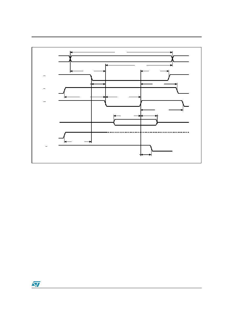
M29W640FT, M29W640FB
7 DC and AC parameters
39/72
Figure 10. Write AC Waveforms, Write Enable Controlled
AI05560
E
G
W
A0-A20/
A
≠
1
DQ0-DQ7/
DQ8-DQ15
VALID
VALID
VCC
tVCHEL
tWHEH
tWHWL
tELWL
tAVWL
tWHGL
tWLAX
tWHDX
tAVAV
tDVWH
tWLWH
tGHWL
RB
tWHRL
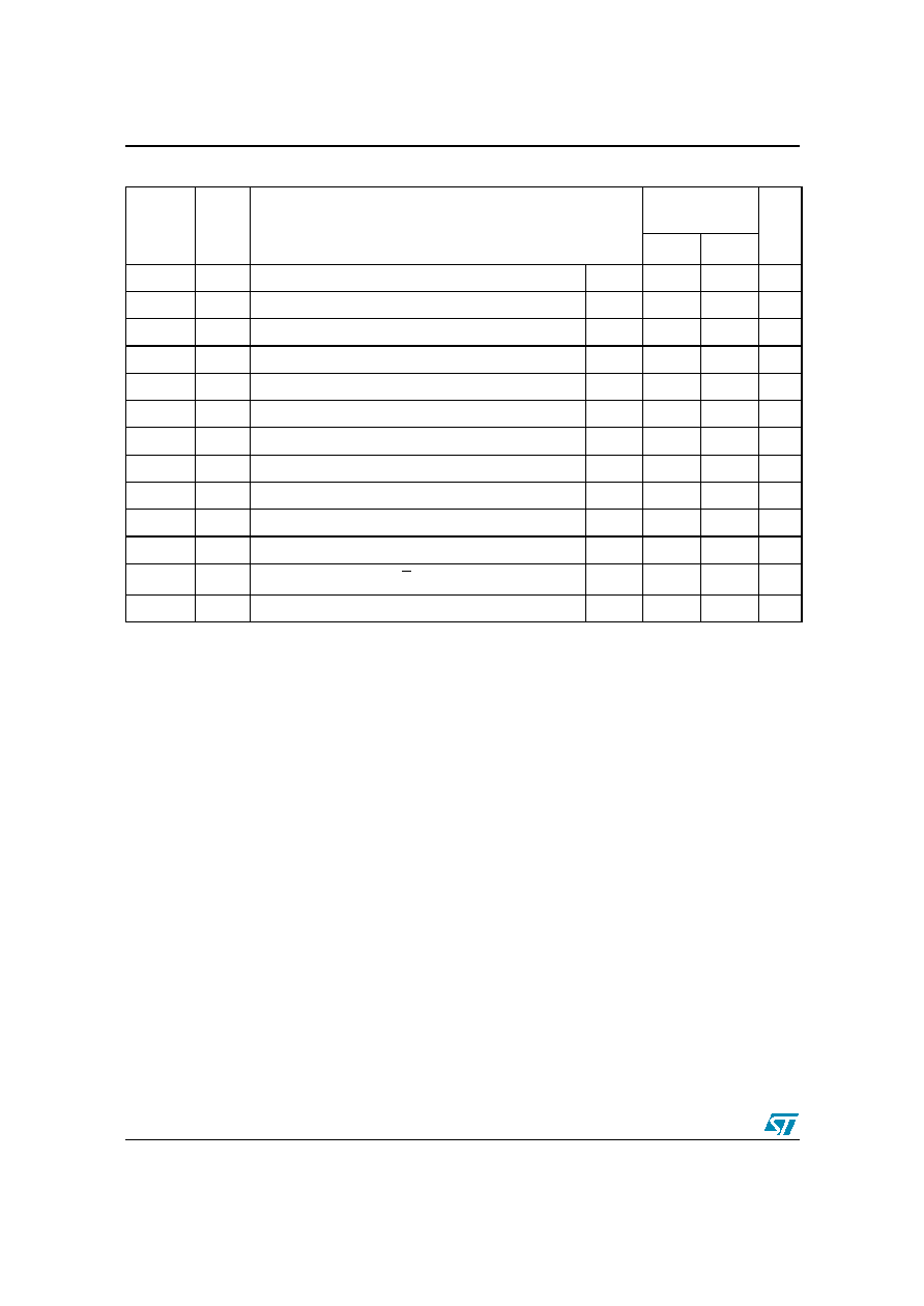
7 DC and AC parameters
M29W640FT, M29W640FB
40/72
Table 14.
Write AC Characteristics, Write Enable Controlled
Symbol
Alt
Parameter
M29W640FT,
M29W640FB
Unit
60
70
t
AVAV
t
WC
Address Valid to Next Address Valid
Min
60
70
ns
t
ELWL
t
CS
Chip Enable Low to Write Enable Low
Min
0
0
ns
t
WLWH
t
WP
Write Enable Low to Write Enable High
Min
45
45
ns
t
DVWH
t
DS
Input Valid to Write Enable High
Min
45
45
ns
t
WHDX
t
DH
Write Enable High to Input Transition
Min
0
0
ns
t
WHEH
t
CH
Write Enable High to Chip Enable High
Min
0
0
ns
t
WHWL
t
WPH
Write Enable High to Write Enable Low
Min
30
30
ns
t
AVWL
t
AS
Address Valid to Write Enable Low
Min
0
0
ns
t
WLAX
t
AH
Write Enable Low to Address Transition
Min
45
45
ns
t
GHWL
Output Enable High to Write Enable Low
Min
0
0
ns
t
WHGL
t
OEH
Write Enable High to Output Enable Low
Min
0
0
ns
t
WHRL
(1)
1. Sampled only, not 100% tested.
t
BUSY
Program/Erase Valid to RB Low
Max
30
30
ns
t
VCHEL
t
VCS
V
CC
High to Chip Enable Low
Min
50
50
µ
s
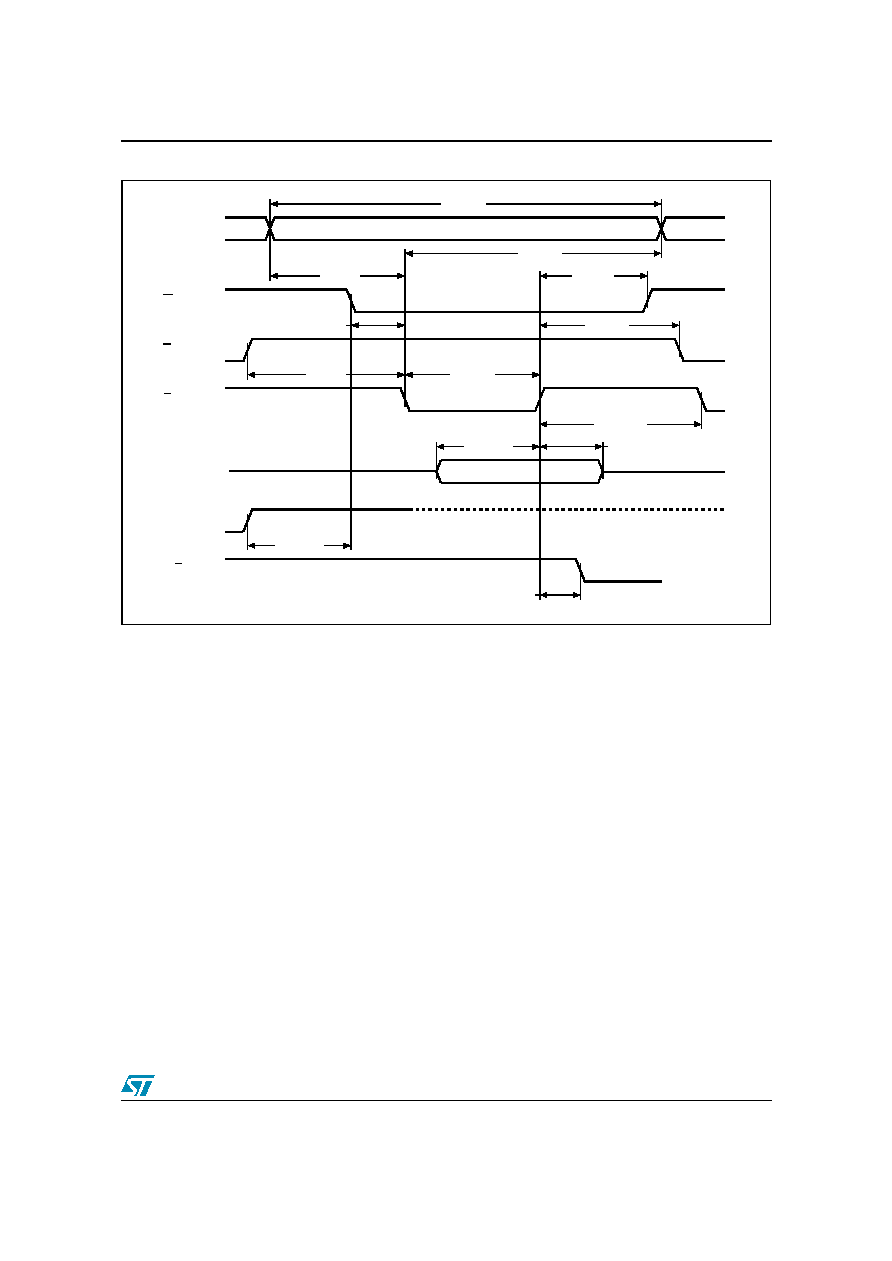
M29W640FT, M29W640FB
7 DC and AC parameters
41/72
Figure 11. Write AC Waveforms, Chip Enable Controlled
AI05561
E
G
W
A0-A20/
A
≠
1
DQ0-DQ7/
DQ8-DQ15
VALID
VALID
VCC
tVCHWL
tEHWH
tEHEL
tWLEL
tAVEL
tEHGL
tELAX
tEHDX
tAVAV
tDVEH
tELEH
tGHEL
RB
tEHRL
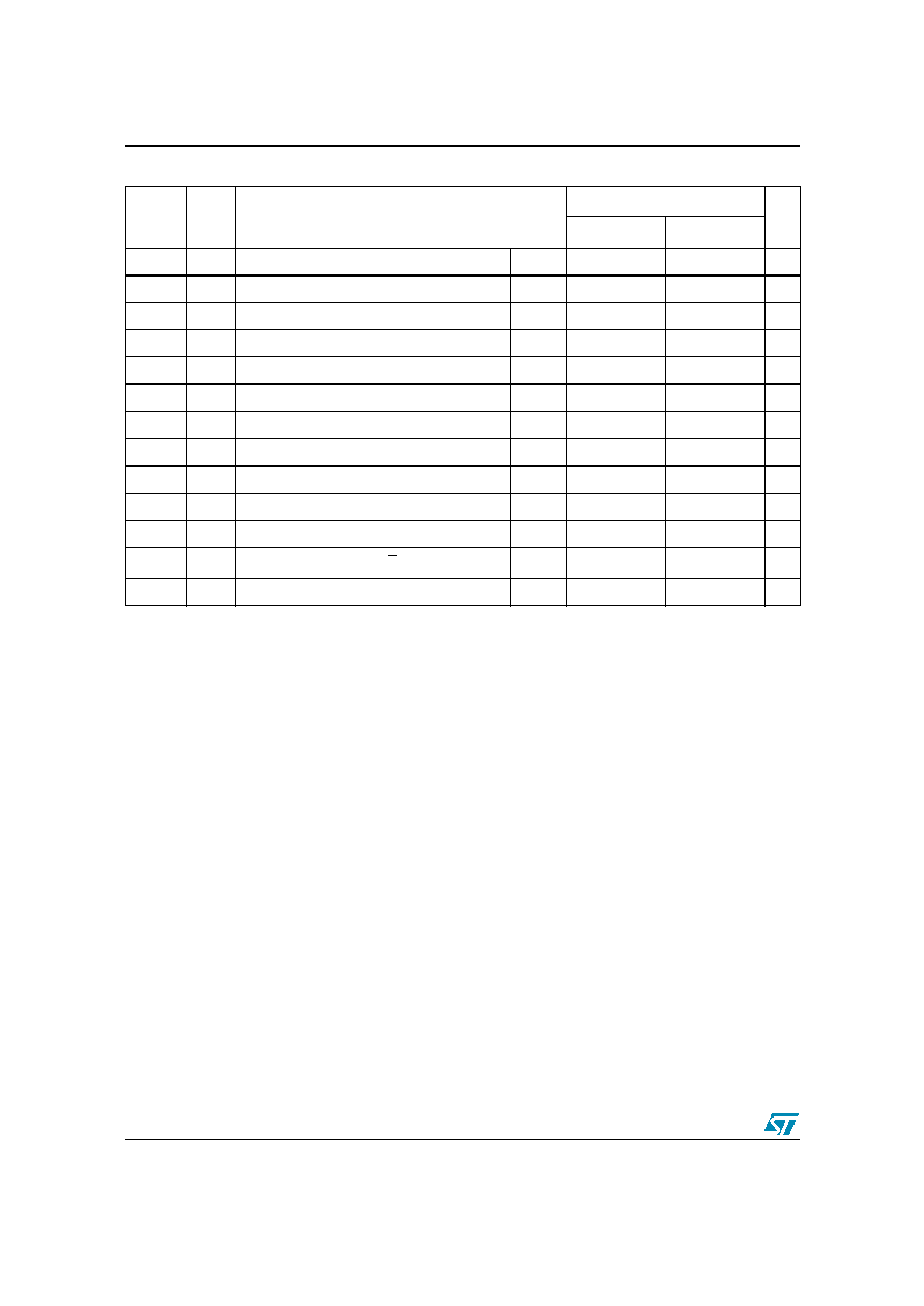
7 DC and AC parameters
M29W640FT, M29W640FB
42/72
Table 15.
Write AC Characteristics, Chip Enable Controlled
Symbol
Alt
Parameter
M29W640FT, M29W640FB
Unit
60
70
t
AVAV
t
WC
Address Valid to Next Address Valid
Min
60
70
ns
t
WLEL
t
WS
Write Enable Low to Chip Enable Low
Min
0
0
ns
t
ELEH
t
CP
Chip Enable Low to Chip Enable High
Min
45
45
ns
t
DVEH
t
DS
Input Valid to Chip Enable High
Min
45
45
ns
t
EHDX
t
DH
Chip Enable High to Input Transition
Min
0
0
ns
t
EHWH
t
WH
Chip Enable High to Write Enable High
Min
0
0
ns
t
EHEL
t
CPH
Chip Enable High to Chip Enable Low
Min
30
30
ns
t
AVEL
t
AS
Address Valid to Chip Enable Low
Min
0
0
ns
t
ELAX
t
AH
Chip Enable Low to Address Transition
Min
45
45
ns
t
GHEL
Output Enable High Chip Enable Low
Min
0
0
ns
t
EHGL
t
OEH
Chip Enable High to Output Enable Low
Min
0
0
ns
t
EHRL
(1)
1. Sampled only, not 100% tested.
t
BUSY
Program/Erase Valid to RB Low
Max
30
30
ns
t
VCHWL
t
VCS
V
CC
High to Write Enable Low
Min
50
50
µ
s
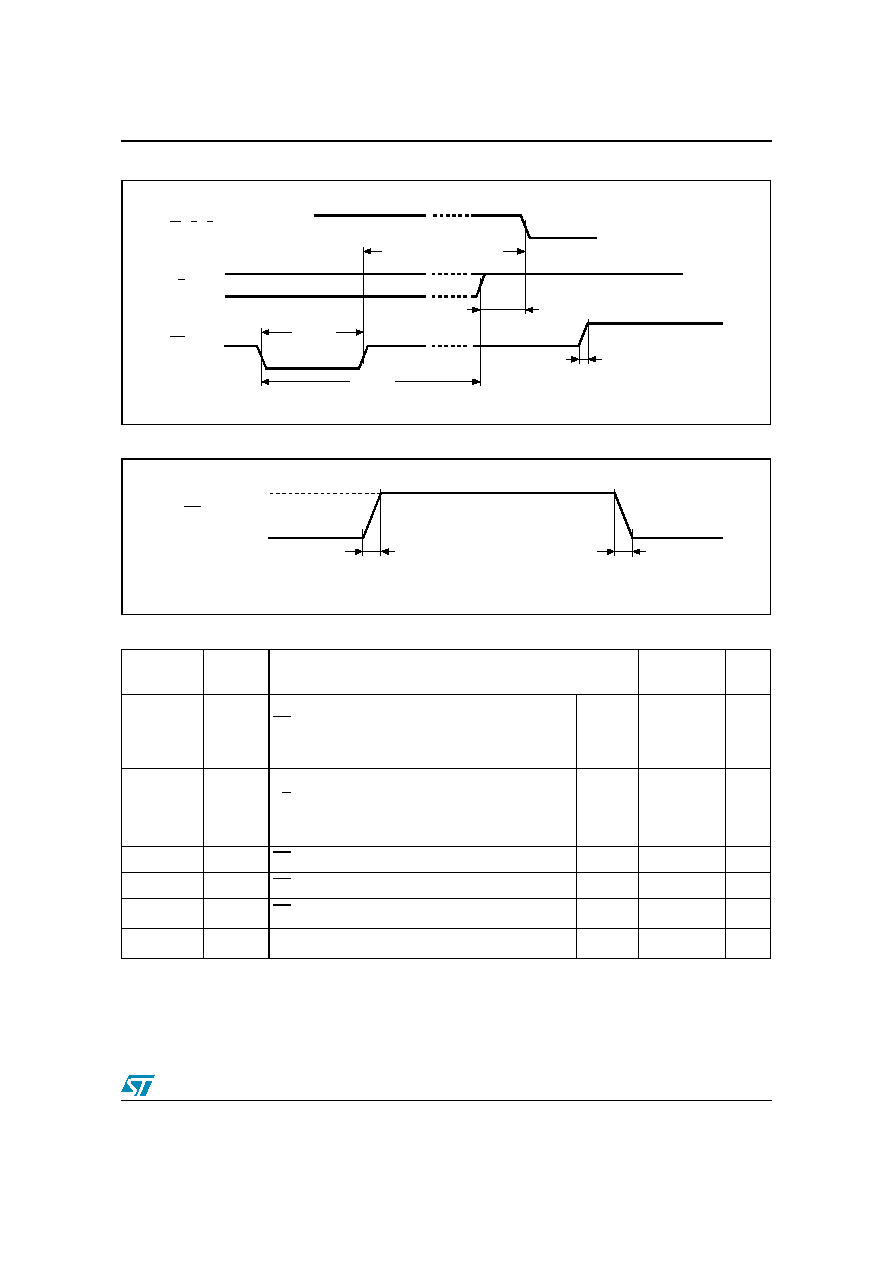
M29W640FT, M29W640FB
7 DC and AC parameters
43/72
Figure 12. Reset/Block Temporary Unprotect AC Waveforms
Figure 13. Accelerated Program Timing Waveforms
Table 16.
Reset/Block Temporary Unprotect AC Characteristics
Symbol
Alt
Parameter
M29W640FT,
M29W640FB
Unit
t
PHWL
(1)
t
PHEL
t
PHGL
(1)
1. Sampled only, not 100% tested.
t
RH
RP High to Write Enable Low, Chip Enable Low,
Output Enable Low
Min
50
ns
t
RHWL
(1)
t
RHEL
(1)
t
RHGL
(1)
t
RB
RB High to Write Enable Low, Chip Enable Low,
Output Enable Low
Min
0
ns
t
PLPX
t
RP
RP Pulse Width
Min
500
ns
t
PLYH
t
READY
RP Low to Read Mode
Max
50
µ
s
t
PHPHH
(1)
t
VIDR
RP Rise Time to V
ID
Min
500
ns
t
VHVPP
(1)
V
PP
Rise and Fall Time
Min
250
ns
AI02931B
RB
W,
RP
tPLPX
tPHWL, tPHEL, tPHGL
tPLYH
tPHPHH
E, G
tRHWL, tRHEL, tRHGL
AI05563
VPP/WP
VPP
VIL or VIH
tVHVPP
tVHVPP
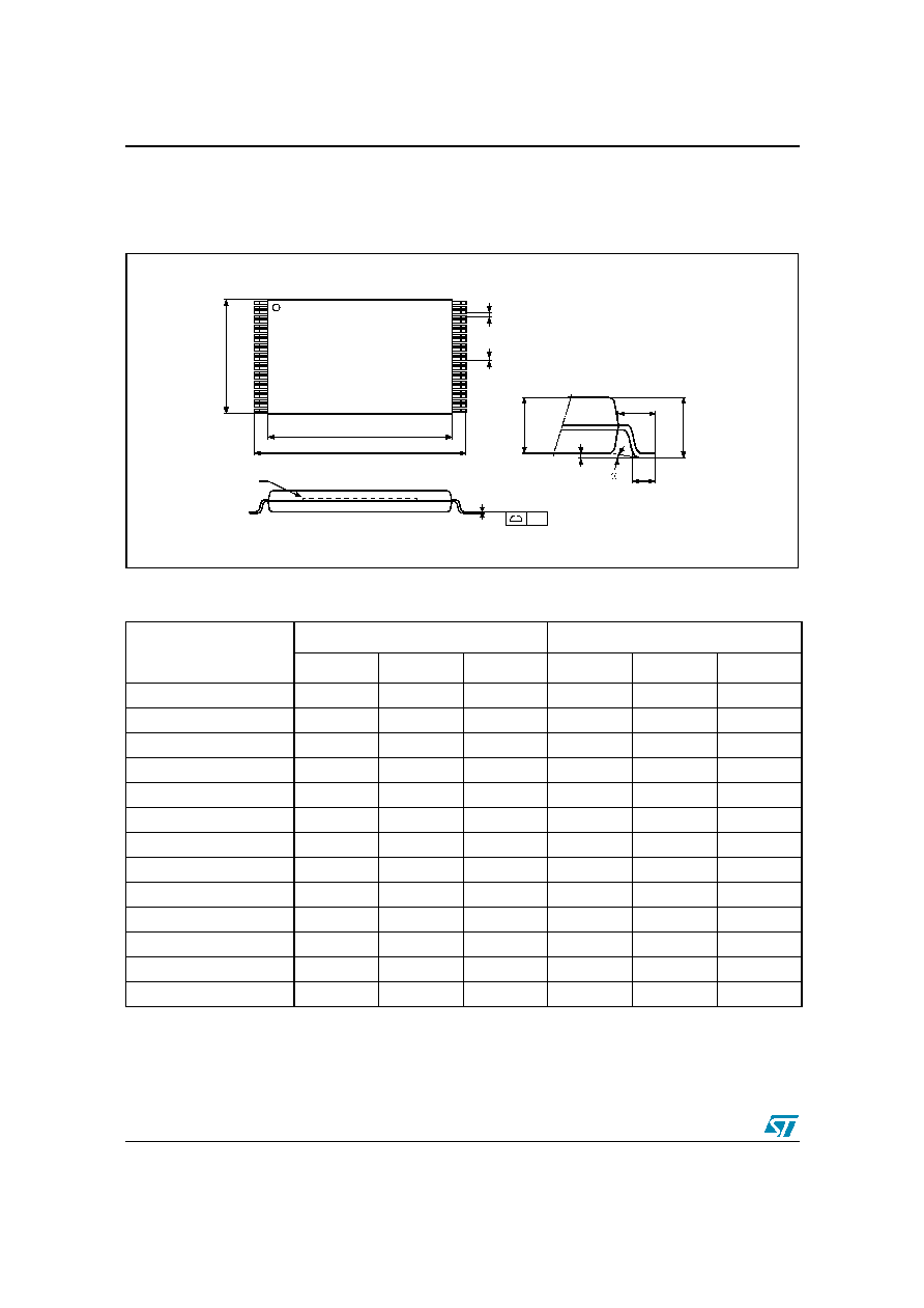
8 Package mechanical
M29W640FT, M29W640FB
44/72
8
Package mechanical
Figure 14. TSOP48
≠
48 lead Plastic Thin Small Outline, 12 x 20mm, Package Outline
1. Drawing is not to scale.
Table 17.
TSOP48
≠
48 lead Plastic Thin Small Outline, 12 x 20mm, Package Mechanical Data
Symbol
millimeters
inches
Typ
Min
Max
Typ
Min
Max
A
1.200
0.0472
A1
0.100
0.050
0.150
0.0039
0.0020
0.0059
A2
1.000
0.950
1.050
0.0394
0.0374
0.0413
B
0.220
0.170
0.270
0.0087
0.0067
0.0106
C
0.100
0.210
0.0039
0.0083
CP
0.100
0.0039
D1
12.000
11.900
12.100
0.4724
0.4685
0.4764
E
20.000
19.800
20.200
0.7874
0.7795
0.7953
E1
18.400
18.300
18.500
0.7244
0.7205
0.7283
e
0.500
≠
≠
0.0197
≠
≠
L
0.600
0.500
0.700
0.0236
0.0197
0.0276
L1
0.800
0.0315
a
3
0
5
3
0
5
TSOP-G
B
e
DIE
C
L
A1
E1
E
A
A2
1
24
48
25
D1
L1
CP

M29W640FT, M29W640FB
8 Package mechanical
45/72
Figure 15. TFBGA48 6x8mm - 6x8 active ball array, 0.8mm pitch, Package Outline
1. Drawing is not to scale.
Table 18.
TFBGA48 6x8mm - 6x8 active ball array, 0.8mm pitch, Package Mechanical Data
Symbol
millimeters
inches
Typ
Min
Max
Typ
Min
Max
A
1.200
0.0472
A1
0.260
0.0102
A2
0.900
0.0354
b
0.350
0.450
0.0138
0.0177
D
6.000
5.900
6.100
0.2362
0.2323
0.2402
D1
4.000
≠
≠
0.1575
≠
≠
ddd
0.100
0.0039
E
8.000
7.900
8.100
0.3150
0.3110
0.3189
E1
5.600
≠
≠
0.2205
≠
≠
e
0.800
≠
≠
0.0315
≠
≠
FD
1.000
≠
≠
0.0394
≠
≠
FE
1.200
≠
≠
0.0472
≠
≠
SD
0.400
≠
≠
0.0157
≠
≠
SE
0.400
≠
≠
0.0157
≠
≠
E1
E
D1
D
e
b
A2
A1
A
BGA-Z32
ddd
FD
FE
SD
SE
e
BALL "A1"

9 Part Numbering
M29W640FT, M29W640FB
46/72
9
Part Numbering
Table 19.
Ordering Information Scheme
Note: This product is also available with the Extended Block factory locked. For further details
and ordering information contact your nearest ST sales office.
Devices are shipped from the factory with the memory content bits erased to 1. For a list of
available options (Speed, Package, etc.) or for further information on any aspect of this device,
please contact your nearest ST Sales Office.
Example:
M29W640FB
70
N
6
F
Device Type
M29
Operating Voltage
W = V
CC
= 2.7 to 3.6V
Device Function
640F = 64 Mbit (x8/x16), Boot Block
Array Matrix
T = Top Boot
B = Bottom Boot
Speed
60 = 60ns
70 = 70ns
Package
N = TSOP48: 12 x 20 mm
ZA = TFBGA48: 6x8mm, 0.80 mm pitch
Temperature Range
6 = 40 to 85
∞
C
Option
E = ECOPACK Package, Standard Packing
F = ECOPACK Package, Tape & Reel Packing

M29W640FT, M29W640FB
9 Part Numbering
47/72
Appendix A Block addresses
Table 20.
Top Boot Block Addresses, M29W640FT
Block
KBytes/
KWords
Protection Block
Group
(x8)
(x16)
0
64/32
Protection Group
000000h
≠
00FFFFh
(1)
000000h
≠
007FFFh
(1)
1
64/32
010000h
≠
01FFFFh
008000h
≠
00FFFFh
2
64/32
020000h
≠
02FFFFh
010000h
≠
017FFFh
3
64/32
030000h
≠
03FFFFh
018000h
≠
01FFFFh
4
64/32
Protection Group
040000h
≠
04FFFFh
020000h
≠
027FFFh
5
64/32
050000h
≠
05FFFFh
028000h
≠
02FFFFh
6
64/32
060000h
≠
06FFFFh
030000h
≠
037FFFh
7
64/32
070000h
≠
07FFFFh
038000h
≠
03FFFFh
8
64/32
Protection Group
080000h
≠
08FFFFh
040000h
≠
047FFFh
9
64/32
090000h
≠
09FFFFh
048000h
≠
04FFFFh
10
64/32
0A0000h
≠
0AFFFFh
050000h
≠
057FFFh
11
64/32
0B0000h
≠
0BFFFFh
058000h
≠
05FFFFh
12
64/32
Protection Group
0C0000h
≠
0CFFFFh
060000h
≠
067FFFh
13
64/32
0D0000h
≠
0DFFFFh
068000h
≠
06FFFFh
14
64/32
0E0000h
≠
0EFFFFh
070000h
≠
077FFFh
15
64/32
0F0000h
≠
0FFFFFh
078000h
≠
07FFFFh
16
64/32
Protection Group
100000h
≠
10FFFFh
080000h
≠
087FFFh
17
64/32
110000h
≠
11FFFFh
088000h
≠
08FFFFh
18
64/32
120000h
≠
12FFFFh
090000h
≠
097FFFh
19
64/32
130000h
≠
13FFFFh
098000h
≠
09FFFFh
20
64/32
Protection Group
140000h
≠
14FFFFh
0A0000h
≠
0A7FFFh
21
64/32
150000h
≠
15FFFFh
0A8000h
≠
0AFFFFh
22
64/32
160000h
≠
16FFFFh
0B0000h
≠
0B7FFFh
23
64/32
170000h
≠
17FFFFh
0B8000h
≠
0BFFFFh
24
64/32
Protection Group
180000h
≠
18FFFFh
0C0000h
≠
0C7FFFh
25
64/32
190000h
≠
19FFFFh
0C8000h
≠
0CFFFFh
26
64/32
1A0000h
≠
1AFFFFh
0D0000h
≠
0D7FFFh
27
64/32
1B0000h
≠
1BFFFFh
0D8000h
≠
0DFFFFh
9 Part Numbering
M29W640FT, M29W640FB
48/72
28
64/32
Protection Group
1C0000h
≠
1CFFFFh
0E0000h
≠
0E7FFFh
29
64/32
1D0000h
≠
1DFFFFh
0E8000h
≠
0EFFFFh
30
64/32
1E0000h
≠
1EFFFFh
0F0000h
≠
0F7FFFh
31
64/32
1F0000h
≠
1FFFFFh
0F8000h
≠
0FFFFFh
32
64/32
Protection Group
200000h
≠
20FFFFh
100000h
≠
107FFFh
33
64/32
210000h
≠
21FFFFh
108000h
≠
10FFFFh
34
64/32
220000h
≠
22FFFFh
110000h
≠
117FFFh
35
64/32
230000h
≠
23FFFFh
118000h
≠
11FFFFh
36
64/32
Protection Group
240000h
≠
24FFFFh
120000h
≠
127FFFh
37
64/32
250000h
≠
25FFFFh
128000h
≠
12FFFFh
38
64/32
260000h
≠
26FFFFh
130000h
≠
137FFFh
39
64/32
270000h
≠
27FFFFh
138000h
≠
13FFFFh
40
64/32
Protection Group
280000h
≠
28FFFFh
140000h
≠
147FFFh
41
64/32
290000h
≠
29FFFFh
148000h
≠
14FFFFh
42
64/32
2A0000h
≠
2AFFFFh
150000h
≠
157FFFh
43
64/32
2B0000h
≠
2BFFFFh
158000h
≠
15FFFFh
44
64/32
Protection Group
2C0000h
≠
2CFFFFh
160000h
≠
167FFFh
45
64/32
2D0000h
≠
2DFFFFh
168000h
≠
16FFFFh
46
64/32
2E0000h
≠
2EFFFFh
170000h
≠
177FFFh
47
64/32
2F0000h
≠
2FFFFFh
178000h
≠
17FFFFh
48
64/32
Protection Group
300000h
≠
30FFFFh
180000h
≠
187FFFh
49
64/32
310000h
≠
31FFFFh
188000h
≠
18FFFFh
50
64/32
320000h
≠
32FFFFh
190000h
≠
197FFFh
51
64/32
330000h
≠
33FFFFh
198000h
≠
19FFFFh
52
64/32
Protection Group
340000h
≠
34FFFFh
1A0000h
≠
1A7FFFh
53
64/32
350000h
≠
35FFFFh
1A8000h
≠
1AFFFFh
54
64/32
360000h
≠
36FFFFh
1B0000h
≠
1B7FFFh
55
64/32
370000h
≠
37FFFFh
1B8000h
≠
1BFFFFh
56
64/32
Protection Group
380000h
≠
38FFFFh
1C0000h
≠
1C7FFFh
57
64/32
390000h
≠
39FFFFh
1C8000h
≠
1CFFFFh
58
64/32
3A0000h
≠
3AFFFFh
1D0000h
≠
1D7FFFh
59
64/32
3B0000h
≠
3BFFFFh
1D8000h
≠
1DFFFFh
Block
KBytes/
KWords
Protection Block
Group
(x8)
(x16)
M29W640FT, M29W640FB
9 Part Numbering
49/72
60
64/32
Protection Group
3C0000h
≠
3CFFFFh
1E0000h
≠
1E7FFFh
61
64/32
3D0000h
≠
3DFFFFh
1E8000h
≠
1EFFFFh
62
64/32
3E0000h
≠
3EFFFFh
1F0000h
≠
1F7FFFh
63
64/32
3F0000h
≠
3FFFFFh
1F8000h
≠
1FFFFFh
64
64/32
Protection Group
400000h
≠
40FFFFh
200000h
≠
207FFFh
65
64/32
410000h
≠
41FFFFh
208000h
≠
20FFFFh
66
64/32
420000h
≠
42FFFFh
210000h
≠
217FFFh
67
64/32
430000h
≠
43FFFFh
218000h
≠
21FFFFh
68
64/32
Protection Group
440000h
≠
44FFFFh
220000h
≠
227FFFh
69
64/32
450000h
≠
45FFFFh
228000h
≠
22FFFFh
70
64/32
460000h
≠
46FFFFh
230000h
≠
237FFFh
71
64/32
470000h
≠
47FFFFh
238000h
≠
23FFFFh
72
64/32
Protection Group
480000h
≠
48FFFFh
240000h
≠
247FFFh
73
64/32
490000h
≠
49FFFFh
248000h
≠
24FFFFh
74
64/32
4A0000h
≠
4AFFFFh
250000h
≠
257FFFh
75
64/32
4B0000h
≠
4BFFFFh
258000h
≠
25FFFFh
76
64/32
Protection Group
4C0000h
≠
4CFFFFh
260000h
≠
267FFFh
77
64/32
4D0000h
≠
4DFFFFh
268000h
≠
26FFFFh
78
64/32
4E0000h
≠
4EFFFFh
270000h
≠
277FFFh
79
64/32
4F0000h
≠
4FFFFFh
278000h
≠
27FFFFh
80
64/32
Protection Group
500000h
≠
50FFFFh
280000h
≠
287FFFh
81
64/32
510000h
≠
51FFFFh
288000h
≠
28FFFFh
82
64/32
520000h
≠
52FFFFh
290000h
≠
297FFFh
83
64/32
530000h
≠
53FFFFh
298000h
≠
29FFFFh
84
64/32
Protection Group
540000h
≠
54FFFFh
2A0000h
≠
2A7FFFh
85
64/32
550000h
≠
55FFFFh
2A8000h
≠
2AFFFFh
86
64/32
560000h
≠
56FFFFh
2B0000h
≠
2B7FFFh
87
64/32
570000h
≠
57FFFFh
2B8000h
≠
2BFFFFh
88
64/32
Protection Group
580000h
≠
58FFFFh
2C0000h
≠
2C7FFFh
89
64/32
590000h
≠
59FFFFh
2C8000h
≠
2CFFFFh
90
64/32
5A0000h
≠
5AFFFFh
2D0000h
≠
2D7FFFh
91
64/32
5B0000h
≠
5BFFFFh
2D8000h
≠
2DFFFFh
Block
KBytes/
KWords
Protection Block
Group
(x8)
(x16)

9 Part Numbering
M29W640FT, M29W640FB
50/72
92
64/32
Protection Group
5C0000h
≠
5CFFFFh
2E0000h
≠
2E7FFFh
93
64/32
5D0000h
≠
5DFFFFh
2E8000h
≠
2EFFFFh
94
64/32
5E0000h
≠
5EFFFFh
2F0000h
≠
2F7FFFh
95
64/32
5F0000h
≠
5FFFFFh
2F8000h
≠
2FFFFFh
96
64/32
Protection Group
600000h
≠
60FFFFh
300000h
≠
307FFFh
97
64/32
610000h
≠
61FFFFh
308000h
≠
30FFFFh
98
64/32
620000h
≠
62FFFFh
310000h
≠
317FFFh
99
64/32
630000h
≠
63FFFFh
318000h
≠
31FFFFh
100
64/32
Protection Group
640000h
≠
64FFFFh
320000h
≠
327FFFh
101
64/32
650000h
≠
65FFFFh
328000h
≠
32FFFFh
102
64/32
660000h
≠
66FFFFh
330000h
≠
337FFFh
103
64/32
670000h
≠
67FFFFh
338000h
≠
33FFFFh
104
64/32
Protection Group
680000h
≠
68FFFFh
340000h
≠
347FFFh
105
64/32
690000h
≠
69FFFFh
348000h
≠
34FFFFh
106
64/32
6A0000h
≠
6AFFFFh
350000h
≠
357FFFh
107
64/32
6B0000h
≠
6BFFFFh
358000h
≠
35FFFFh
108
64/32
Protection Group
6C0000h
≠
6CFFFFh
360000h
≠
367FFFh
109
64/32
6D0000h
≠
6DFFFFh
368000h
≠
36FFFFh
110
64/32
6E0000h
≠
6EFFFFh
370000h
≠
377FFFh
111
64/32
6F0000h
≠
6FFFFFh
378000h
≠
37FFFFh
112
64/32
Protection Group
700000h
≠
70FFFFh
380000h
≠
387FFFh
113
64/32
710000h
≠
71FFFFh
388000h
≠
38FFFFh
114
64/32
720000h
≠
72FFFFh
390000h
≠
397FFFh
115
64/32
730000h
≠
73FFFFh
398000h
≠
39FFFFh
116
64/32
Protection Group
740000h
≠
74FFFFh
3A0000h
≠
3A7FFFh
117
64/32
750000h
≠
75FFFFh
3A8000h
≠
3AFFFFh
118
64/32
760000h
≠
76FFFFh
3B0000h
≠
3B7FFFh
119
64/32
770000h
≠
77FFFFh
3B8000h
≠
3BFFFFh
120
64/32
Protection Group
780000h
≠
78FFFFh
3C0000h
≠
3C7FFFh
121
64/32
790000h
≠
79FFFFh
3C8000h
≠
3CFFFFh
122
64/32
7A0000h
≠
7AFFFFh
3D0000h
≠
3D7FFFh
123
64/32
7B0000h
≠
7BFFFFh
3D8000h
≠
3DFFFFh
Block
KBytes/
KWords
Protection Block
Group
(x8)
(x16)
M29W640FT, M29W640FB
9 Part Numbering
51/72
124
64/32
Protection Group
7C0000h
≠
7CFFFFh
3E0000h
≠
3E7FFFh
125
64/32
7D0000h
≠
7DFFFFh
3E8000h
≠
3EFFFFh
126
64/32
7E0000h
≠
7EFFFFh
3F0000h
≠
3F7FFFh
127
8/4
7F0000h
≠
7F1FFFh
3F8000h
≠
3F8FFFh
128
8/4
7F2000h
≠
7F3FFFh
3F9000h
≠
3F9FFFh
129
8/4
7F4000h
≠
7F5FFFh
3FA000h
≠
3FAFFFh
130
8/4
7F6000h
≠
7F7FFFh
3FB000h
≠
3FBFFFh
131
8/4
7F8000h
≠
7F9FFFh
3FC000h
≠
3FCFFFh
132
8/4
7FA000h
≠
7FBFFFh
3FD000h
≠
3FDFFFh
133
8/4
7FC000h
≠
7FDFFFh
3FE000h
≠
3FEFFFh
134
8/4
7FE000h
≠
7FFFFFh
3FF000h
≠
3FFFFFh
1. Used as the Extended Block Addresses in Extended Block mode.
Block
KBytes/
KWords
Protection Block
Group
(x8)
(x16)
9 Part Numbering
M29W640FT, M29W640FB
52/72
Table 21.
Bottom Boot Block Addresses, M29W640FB
Block
KBytes/
KWords
Protection Block
Group
(x8)
(x16)
0
8/4
Protection Group
000000h-001FFFh
(1)
000000h
≠
000FFFh
(1)
1
8/4
002000h-003FFFh
001000h
≠
001FFFh
2
8/4
004000h-005FFFh
002000h
≠
002FFFh
3
8/4
006000h-007FFFh
003000h
≠
003FFFh
4
8/4
008000h-009FFFh
004000h
≠
004FFFh
5
8/4
00A000h-00BFFFh
005000h
≠
005FFFh
6
8/4
00C000h-00DFFFh
006000h
≠
006FFFh
7
8/4
00E000h-00FFFFh
007000h
≠
007FFFh
8
64/32
010000h-01FFFFh
008000h
≠
00FFFFh
9
64/32
020000h-02FFFFh
010000h
≠
017FFFh
10
64/32
030000h-03FFFFh
018000h
≠
01FFFFh
11
64/32
Protection Group
040000h-04FFFFh
020000h
≠
027FFFh
12
64/32
050000h-05FFFFh
028000h
≠
02FFFFh
13
64/32
060000h-06FFFFh
030000h
≠
037FFFh
14
64/32
070000h-07FFFFh
038000h
≠
03FFFFh
15
64/32
Protection Group
080000h-08FFFFh
040000h
≠
047FFFh
16
64/32
090000h-09FFFFh
048000h
≠
04FFFFh
17
64/32
0A0000h-0AFFFFh
050000h
≠
057FFFh
18
64/32
0B0000h-0BFFFFh
058000h
≠
05FFFFh
19
64/32
Protection Group
0C0000h-0CFFFFh
060000h
≠
067FFFh
20
64/32
0D0000h-0DFFFFh
068000h
≠
06FFFFh
21
64/32
0E0000h-0EFFFFh
070000h
≠
077FFFh
22
64/32
0F0000h-0FFFFFh
078000h
≠
07FFFFh
23
64/32
Protection Group
100000h-10FFFFh
080000h
≠
087FFFh
24
64/32
110000h-11FFFFh
088000h
≠
08FFFFh
25
64/32
120000h-12FFFFh
090000h
≠
097FFFh
26
64/32
130000h-13FFFFh
098000h
≠
09FFFFh
27
64/32
Protection Group
140000h-14FFFFh
0A0000h
≠
0A7FFFh
28
64/32
150000h-15FFFFh
0A8000h
≠
0AFFFFh
29
64/32
160000h-16FFFFh
0B0000h
≠
0B7FFFh
30
64/32
170000h-17FFFFh
0B8000h
≠
0BFFFFh

M29W640FT, M29W640FB
9 Part Numbering
53/72
31
64/32
Protection Group
180000h-18FFFFh
0C0000h
≠
0C7FFFh
32
64/32
190000h-19FFFFh
0C8000h
≠
0CFFFFh
33
64/32
1A0000h-1AFFFFh
0D0000h
≠
0D7FFFh
34
64/32
1B0000h-1BFFFFh
0D8000h
≠
0DFFFFh
35
64/32
Protection Group
1C0000h-1CFFFFh
0E0000h
≠
0E7FFFh
36
64/32
1D0000h-1DFFFFh
0E8000h
≠
0EFFFFh
37
64/32
1E0000h-1EFFFFh
0F0000h
≠
0F7FFFh
38
64/32
1F0000h-1FFFFFh
0F8000h
≠
0FFFFFh
39
64/32
Protection Group
200000h-20FFFFh
100000h
≠
107FFFh
40
64/32
210000h-21FFFFh
108000h
≠
10FFFFh
41
64/32
220000h-22FFFFh
110000h
≠
117FFFh
42
64/32
230000h-23FFFFh
118000h
≠
11FFFFh
43
64/32
Protection Group
240000h-24FFFFh
120000h
≠
127FFFh
44
64/32
250000h-25FFFFh
128000h
≠
12FFFFh
45
64/32
260000h-26FFFFh
130000h
≠
137FFFh
46
64/32
270000h-27FFFFh
138000h
≠
13FFFFh
47
64/32
Protection Group
280000h-28FFFFh
140000h
≠
147FFFh
48
64/32
290000h-29FFFFh
148000h
≠
14FFFFh
49
64/32
2A0000h-2AFFFFh
150000h
≠
157FFFh
50
64/32
2B0000h-2BFFFFh
158000h
≠
15FFFFh
51
64/32
Protection Group
2C0000h-2CFFFFh
160000h
≠
167FFFh
52
64/32
2D0000h-2DFFFFh
168000h
≠
16FFFFh
53
64/32
2E0000h-2EFFFFh
170000h
≠
177FFFh
54
64/32
2F0000h-2FFFFFh
178000h
≠
17FFFFh
55
64/32
Protection Group
300000h-30FFFFh
180000h
≠
187FFFh
56
64/32
310000h-31FFFFh
188000h
≠
18FFFFh
57
64/32
320000h-32FFFFh
190000h
≠
197FFFh
58
64/32
330000h-33FFFFh
198000h
≠
19FFFFh
59
64/32
Protection Group
340000h-34FFFFh
1A0000h
≠
1A7FFFh
60
64/32
350000h-35FFFFh
1A8000h
≠
1AFFFFh
61
64/32
360000h-36FFFFh
1B0000h
≠
1B7FFFh
62
64/32
370000h-37FFFFh
1B8000h
≠
1BFFFFh
Block
KBytes/
KWords
Protection Block
Group
(x8)
(x16)
9 Part Numbering
M29W640FT, M29W640FB
54/72
63
64/32
Protection Group
380000h-38FFFFh
1C0000h
≠
1C7FFFh
64
64/32
390000h-39FFFFh
1C8000h
≠
1CFFFFh
65
64/32
3A0000h-3AFFFFh
1D0000h
≠
1D7FFFh
66
64/32
3B0000h-3BFFFFh
1D8000h
≠
1DFFFFh
67
64/32
Protection Group
3C0000h-3CFFFFh
1E0000h
≠
1E7FFFh
68
64/32
3D0000h-3DFFFFh
1E8000h
≠
1EFFFFh
69
64/32
3E0000h-3EFFFFh
1F0000h
≠
1F7FFFh
70
64/32
3F0000h-3FFFFFh
1F8000h
≠
1FFFFFh
71
64/32
Protection Group
400000h-40FFFFh
200000h
≠
207FFFh
72
64/32
410000h-41FFFFh
208000h
≠
20FFFFh
73
64/32
420000h-42FFFFh
210000h
≠
217FFFh
74
64/32
430000h-43FFFFh
218000h
≠
21FFFFh
75
64/32
Protection Group
440000h-44FFFFh
220000h
≠
227FFFh
76
64/32
450000h-45FFFFh
228000h
≠
22FFFFh
77
64/32
460000h-46FFFFh
230000h
≠
237FFFh
78
64/32
470000h-47FFFFh
238000h
≠
23FFFFh
79
64/32
Protection Group
480000h-48FFFFh
240000h
≠
247FFFh
80
64/32
490000h-49FFFFh
248000h
≠
24FFFFh
81
64/32
4A0000h-4AFFFFh
250000h
≠
257FFFh
82
64/32
4B0000h-4BFFFFh
258000h
≠
25FFFFh
83
64/32
Protection Group
4C0000h-4CFFFFh
260000h
≠
267FFFh
84
64/32
4D0000h-4DFFFFh
268000h
≠
26FFFFh
85
64/32
4E0000h-4EFFFFh
270000h
≠
277FFFh
86
64/32
4F0000h-4FFFFFh
278000h
≠
27FFFFh
87
64/32
Protection Group
500000h-50FFFFh
280000h
≠
287FFFh
88
64/32
510000h-51FFFFh
288000h
≠
28FFFFh
89
64/32
520000h-52FFFFh
290000h
≠
297FFFh
90
64/32
530000h-53FFFFh
298000h
≠
29FFFFh
91
64/32
Protection Group
540000h-54FFFFh
2A0000h
≠
2A7FFFh
92
64/32
550000h-55FFFFh
2A8000h
≠
2AFFFFh
93
64/32
560000h-56FFFFh
2B0000h
≠
2B7FFFh
94
64/32
570000h-57FFFFh
2B8000h
≠
2BFFFFh
Block
KBytes/
KWords
Protection Block
Group
(x8)
(x16)
M29W640FT, M29W640FB
9 Part Numbering
55/72
95
64/32
Protection Group
580000h-58FFFFh
2C0000h
≠
2C7FFFh
96
64/32
590000h-59FFFFh
2C8000h
≠
2CFFFFh
97
64/32
5A0000h-5AFFFFh
2D0000h
≠
2D7FFFh
98
64/32
5B0000h-5BFFFFh
2D8000h
≠
2DFFFFh
99
64/32
Protection Group
5C0000h-5CFFFFh
2E0000h
≠
2E7FFFh
100
64/32
5D0000h-5DFFFFh
2E8000h
≠
2EFFFFh
101
64/32
5E0000h-5EFFFFh
2F0000h
≠
2F7FFFh
102
64/32
5F0000h-5FFFFFh
2F8000h
≠
2FFFFFh
103
64/32
Protection Group
600000h-60FFFFh
300000h
≠
307FFFh
104
64/32
610000h-61FFFFh
308000h
≠
30FFFFh
105
64/32
620000h-62FFFFh
310000h
≠
317FFFh
106
64/32
630000h-63FFFFh
318000h
≠
31FFFFh
107
64/32
Protection Group
640000h-64FFFFh
320000h
≠
327FFFh
108
64/32
650000h-65FFFFh
328000h
≠
32FFFFh
109
64/32
660000h-66FFFFh
330000h
≠
337FFFh
110
64/32
670000h-67FFFFh
338000h
≠
33FFFFh
111
64/32
Protection Group
680000h-68FFFFh
340000h
≠
347FFFh
112
64/32
690000h-69FFFFh
348000h
≠
34FFFFh
113
64/32
6A0000h-6AFFFFh
350000h
≠
357FFFh
114
64/32
6B0000h-6BFFFFh
358000h
≠
35FFFFh
115
64/32
Protection Group
6C0000h-6CFFFFh
360000h
≠
367FFFh
116
64/32
6D0000h-6DFFFFh
368000h
≠
36FFFFh
117
64/32
6E0000h-6EFFFFh
370000h
≠
377FFFh
118
64/32
6F0000h-6FFFFFh
378000h
≠
37FFFFh
119
64/32
Protection Group
700000h-70FFFFh
380000h
≠
387FFFh
120
64/32
710000h-71FFFFh
388000h
≠
38FFFFh
121
64/32
720000h-72FFFFh
390000h
≠
397FFFh
122
64/32
730000h-73FFFFh
398000h
≠
39FFFFh
123
64/32
Protection Group
740000h-74FFFFh
3A0000h
≠
3A7FFFh
124
64/32
750000h-75FFFFh
3A8000h
≠
3AFFFFh
125
64/32
760000h-76FFFFh
3B0000h
≠
3B7FFFh
126
64/32
770000h-77FFFFh
3B8000h
≠
3BFFFFh
Block
KBytes/
KWords
Protection Block
Group
(x8)
(x16)
9 Part Numbering
M29W640FT, M29W640FB
56/72
127
64/32
Protection Group
780000h-78FFFFh
3C0000h
≠
3C7FFFh
128
64/32
790000h-79FFFFh
3C8000h
≠
3CFFFFh
129
64/32
7A0000h-7AFFFFh
3D0000h
≠
3D7FFFh
130
64/32
7B0000h-7BFFFFh
3D8000h
≠
3DFFFFh
131
64/32
Protection Group
7C0000h-7CFFFFh
3E0000h
≠
3E7FFFh
132
64/32
7D0000h-7DFFFFh
3E8000h
≠
3EFFFFh
133
64/32
7E0000h-7EFFFFh
3F0000h
≠
3F7FFFh
134
64/32
7F0000h-7FFFFFh
3F8000h
≠
3FFFFFh
1. Used as the Extended Block Addresses in Extended Block mode.
Block
KBytes/
KWords
Protection Block
Group
(x8)
(x16)
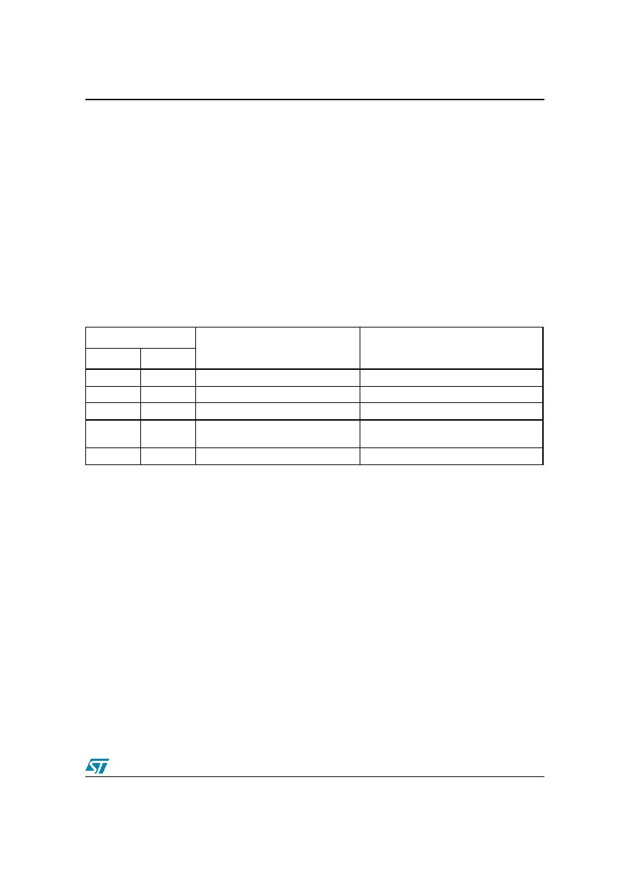
M29W640FT, M29W640FB
9 Part Numbering
57/72
Appendix B Common Flash Interface (CFI)
The Common Flash Interface is a JEDEC approved, standardized data structure that can be
read from the Flash memory device. It allows a system software to query the device to
determine various electrical and timing parameters, density information and functions
supported by the memory. The system can interface easily with the device, enabling the
software to upgrade itself when necessary.
When the CFI Query Command is issued the device enters CFI Query mode and the data
structure is read from the memory. Tables
22
,
23
,
24
,
25
,
26
, and
27
, show the addresses used
to retrieve the data.
The CFI data structure also contains a security area where a 64 bit unique security number is
written (see
Table 27: Security Code Area
). This area can be accessed only in Read mode by
the final user. It is impossible to change the security number after it has been written by ST.
Table 22.
Query Structure Overview
1. Query data are always presented on the lowest order data outputs.
Address
Sub-section Name
Description
x16
x8
10h
20h
CFI Query Identification String
Command set ID and algorithm data offset
1Bh
36h
System Interface Information
Device timing & voltage information
27h
4Eh
Device Geometry Definition
Flash device layout
40h
80h
Primary Algorithm-specific Extended
Query table
Additional information specific to the Primary
Algorithm (optional)
61h
C2h
Security Code Area
64 bit unique device number
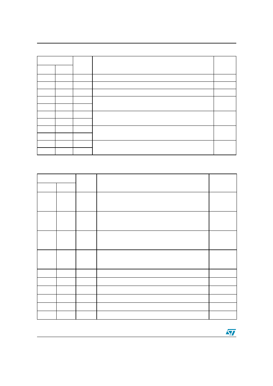
9 Part Numbering
M29W640FT, M29W640FB
58/72
Table 23.
CFI Query Identification String
1. Query data are always presented on the lowest order data outputs (DQ7-DQ0) only. DQ8-DQ15 are
`
0
'
.
Table 24.
CFI Query System Interface Information
Address
Data
Description
Value
x16
x8
10h
20h
0051h
"
Q
"
11h
22h
0052h
Query Unique ASCII String "QRY"
"R"
12h
24h
0059h
"Y"
13h
26h
0002h
Primary Algorithm Command Set and Control Interface ID code 16 bit
ID code defining a specific algorithm
AMD
Compatible
14h
28h
0000h
15h
2Ah
0040h
Address for Primary Algorithm extended Query table (see
Table 26
)
P = 40h
16h
2Ch
0000h
17h
2Eh
0000h
Alternate Vendor Command Set and Control Interface ID Code
second vendor - specified algorithm supported
NA
18h
30h
0000h
19h
32h
0000h
Address for Alternate Algorithm extended Query table
NA
1Ah
34h
0000h
Address
Data
Description
Value
x16
x8
1Bh
36h
0027h
V
CC
Logic Supply Minimum Program/Erase voltage
bit 7 to 4BCD value in volts
bit 3 to 0BCD value in 100 mV
2.7V
1Ch
38h
0036h
V
CC
Logic Supply Maximum Program/Erase voltage
bit 7 to 4BCD value in volts
bit 3 to 0BCD value in 100 mV
3.6V
1Dh
3Ah
00B5h
V
PP
[Programming] Supply Minimum Program/Erase voltage
bit 7 to 4HEX value in volts
bit 3 to 0BCD value in 100 mV
11.5V
1Eh
3Ch
00C5h
V
PP
[Programming] Supply Maximum Program/Erase voltage
bit 7 to 4HEX value in volts
bit 3 to 0BCD value in 100 mV
12.5V
1Fh
3Eh
0004h
Typical timeout per single byte/word program = 2
n
µ
s
16
µ
s
20h
40h
0000h
Typical timeout for minimum size write buffer program = 2
n
µ
s
NA
21h
42h
000Ah
Typical timeout per individual Block Erase = 2
n
ms
1s
22h
44h
0000h
Typical timeout for full Chip Erase = 2
n
ms
NA
23h
46h
0004h
Maximum timeout for byte/word program = 2
n
times typical
256
µ
s
24h
48h
0000h
Maximum timeout for write buffer program = 2
n
times typical
NA
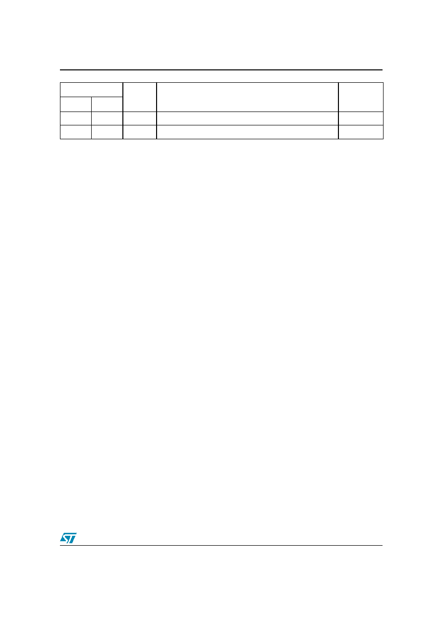
M29W640FT, M29W640FB
9 Part Numbering
59/72
25h
4Ah
0003h
Maximum timeout per individual Block Erase = 2
n
times typical
8s
26h
4Ch
0000h
Maximum timeout for Chip Erase = 2
n
times typical
NA
Address
Data
Description
Value
x16
x8
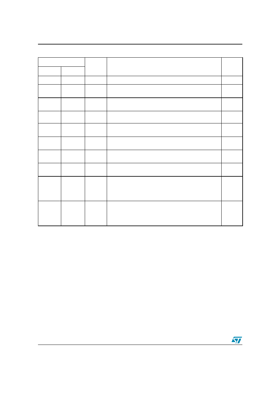
9 Part Numbering
M29W640FT, M29W640FB
60/72
Table 25.
Device Geometry Definition
1. For Bottom Boot devices, Erase Block Region 1 is located from address 000000h to 007FFFh and Erase Block Region 2
from address 008000h to 3FFFFFh.
For Top Boot devices, Erase Block Region 1 is located from address 000000h to 3F7FFFh and Erase Block Region 2 from
address 3F8000h to 3FFFFFh.
Address
Data
Description
Value
x16
x8
27h
4Eh
0017h
Device Size = 2
n
in number of bytes
8 MByte
28h
29h
50h
52h
0002h
0000h
Flash Device Interface Code description
x8, x16
Async.
2Ah
2Bh
54h
56h
0004h
0000h
Maximum number of bytes in multi-byte program or page = 2
n
16 Bytes
2Ch
58h
0002h
Number of Erase Block Regions. It specifies the number of
regions containing contiguous Erase Blocks of the same size.
2
2Dh
2Eh
5Ah
5Ch
0007h
0000h
Region 1 Information
Number of Erase Blocks of identical size = 0007h+1
8
2Fh
30h
5Eh
60h
0020h
0000h
Region 1 Information
Block size in Region 1 = 0020h * 256 byte
8Kbyte
31h
32h
62h
64h
007Eh
0000h
Region 2 Information
Number of Erase Blocks of identical size= 007Eh+1
127
33h
34h
66h
68h
0000h
0001h
Region 2 Information
Block size in Region 2 = 0100h * 256 byte
64Kbyte
35h
36h
37h
38h
6Ah
6Ch
6Eh
70h
0000h
0000h
0000h
0000h
Region 3 Information
Number of Erase Blocks of identical size=007Fh+1
Region 3 Information
Block size in Region 3 = 0000h * 256 byte
0
0
39h
3Ah
3Bh
3Ch
72h
74h
76h
78h
0000h
0000h
0000h
0000h
Region 4 Information
Number of Erase Blocks of Identical size=007Fh+1
Region 4 Information
Block size in Region 4 = 0000h * 256 byte
0
0
M29W640FT, M29W640FB
9 Part Numbering
61/72
Table 26.
Primary Algorithm-Specific Extended Query Table
Address
Data
Description
Value
x16
x8
40h
80h
0050h
Primary Algorithm extended Query table unique ASCII string
"
PRI
"
"P"
41h
82h
0052h
"R"
42h
84h
0049h
"I"
43h
86h
0031h
Major version number, ASCII
"
1
"
44h
88h
0033h
Minor version number, ASCII
"3"
45h
8Ah
0000h
Address Sensitive Unlock (bits 1 to 0)
00h = required, 01h = not required
Silicon Revision Number (bits 7 to 2)
Yes
46h
8Ch
0002h
Erase Suspend
00h = not supported, 01h = Read only, 02 = Read and Write
2
47h
8Eh
0004h
Block Protection
00h = not supported, x = number of blocks per protection group
4
48h
90h
0001h
Temporary Block Unprotect
00h = not supported, 01h = supported
Yes
49h
92h
0004h
Block Protect /Unprotect
04 = M29W640F
04
4Ah
94h
0000h
Simultaneous Operations, 00h = not supported
No
4Bh
96h
0000h
Burst Mode: 00h = not supported, 01h = supported
No
4Ch
98h
0001h
Page Mode: 00h = not supported, 01h = 4 page word, 02h = 8
page word
Yes
4Dh
9Ah
00B5h
V
PP
Supply Minimum Program/Erase voltage
bit 7 to 4 HEX value in volts
bit 3 to 0 BCD value in 100 mV
11.5V
4Eh
9Ch
00C5h
V
PP
Supply Maximum Program/Erase voltage
bit 7 to 4 HEX value in volts
bit 3 to 0 BCD value in 100 mV
12.5V
4Fh
9Eh
0002h
0003h
Top/Bottom Boot Block Flag
02h = Bottom Boot device
03h = Top Boot device
≠
50h
A0h
0001h
Program Suspend
00h = Not Supported
01h = Supported
Supported

9 Part Numbering
M29W640FT, M29W640FB
62/72
Table 27.
Security Code Area
Address
Data
Description
x16
x8
61h
C3h, C2h
XXXX
64 bit: unique device number
62h
C5h, C4h
XXXX
63h
C7h, C6h
XXXX
64h
C9h, C8h
XXXX

M29W640FT, M29W640FB
9 Part Numbering
63/72
Appendix C Extended Memory Block
The M29W640F has an extra block, the Extended Block, that can be accessed using a
dedicated command.
This Extended Block is 128 Words in x16 mode and 256 Bytes in x8 mode. It is used as a
security block to provide a permanent security identification number) or to store additional
information.
The Extended Block is either Factory Locked or Customer Lockable, its status is indicated by bit
DQ7. This bit is permanently set to either
`
1
'
or
`
0
'
at the factory and cannot be changed. When
set to
`
1
'
, it indicates that the device is factory locked and the Extended Block is protected.
When set to
`
0
'
, it indicates that the device is customer lockable and the Extended Block is
unprotected. Bit DQ7 being permanently locked to either
`
1
'
or
`
0
'
is another security feature
which ensures that a customer lockable device cannot be used instead of a factory locked one.
Bit DQ7 is the most significant bit in the Extended Block Verify Code and a specific procedure
must be followed to read it. See
"
Extended Memory Block Verify Code
"
in
Table 3: Bus
Operations, BYTE = VIL
and
Table 4: Bus Operations, BYTE = VIH
, for details of how to read bit
DQ7.
The Extended Block can only be accessed when the device is in Extended Block mode. For
details of how the Extended Block mode is entered and exited, refer to the
Section 4.3.1: Enter
Extended Block command
and
Section 4.3.2: Exit Extended Block command
, and to
Table 5
and
Table 6: Commands, 8-bit mode, BYTE = VIL
.
C.1
Factory Locked Extended Block
In devices where the Extended Block is factory locked, the Security Identification Number is
written to the Extended Block address space (see
Table 28: Extended Block Address and Data
)
in the factory. The DQ7 bit is set to
`
1
'
and the Extended Block cannot be unprotected.
C.2
Customer Lockable Extended Block
A device where the Extended Block is customer lockable is delivered with the DQ7 bit set to
`
0
'
and the Extended Block unprotected. It is up to the customer to program and protect the
Extended Block but care must be taken because the protection of the Extended Block is not
reversible.
There are two ways of protecting the Extended Block:
Issue the Enter Extended Block command to place the device in Extended Block mode,
then use the In-System Technique with RP either at V
IH
or at V
ID
(refer to
Appendix D
,
Section D.2: In-System Technique
and to the corresponding flowcharts,
Figure 18
and
Figure 19
, for a detailed explanation of the technique).
Issue the Enter Extended Block command to place the device in Extended Block mode,
then use the Programmer Technique (refer to
Appendix D
,
Section D.1: Programmer
Technique
and to the corresponding flowcharts,
Figure 16
and
Figure 17
, for a detailed
explanation of the technique).
Once the Extended Block is programmed and protected, the Exit Extended Block command
must be issued to exit the Extended Block mode and return the device to Read mode.

9 Part Numbering
M29W640FT, M29W640FB
64/72
Table 28.
Extended Block Address and Data
Address
Data
x8
x16
Factory Locked
Customer Lockable
000000h-00020Fh
000000h-00000Fh
Security Identification Number
Determined by Customer
000021h-0000FFh
000010h-00007Fh
Unavailable

M29W640FT, M29W640FB
9 Part Numbering
65/72
Appendix D Block Protection
Block protection can be used to prevent any operation from modifying the data stored in the
memory. The blocks are protected in groups, refer to
Appendix A: Block addresses
,
Table 20
and
Table 21
for details of the Protection Groups. Once protected, Program and Erase
operations within the protected group fail to change the data.
There are three techniques that can be used to control Block Protection, these are the
Programmer technique, the In-System technique and Temporary Unprotection. Temporary
Unprotection is controlled by the Reset/Block Temporary Unprotection pin, RP; this is described
in the Signal Descriptions section.
D.1
Programmer Technique
The Programmer technique uses high (V
ID
) voltage levels on some of the bus pins. These
cannot be achieved using a standard microprocessor bus, therefore the technique is
recommended only for use in Programming Equipment.
To protect a group of blocks follow the flowchart in
Figure 16: Programmer Equipment Group
Protect Flowchart
. To unprotect the whole chip it is necessary to protect all of the groups first,
then all groups can be unprotected at the same time. To unprotect the chip follow
Figure 17:
Programmer Equipment Chip Unprotect Flowchart
.
Table 29: Programmer Technique Bus
Operations, BYTE = VIH or VIL
, gives a summary of each operation.
The timing on these flowcharts is critical. Care should be taken to ensure that, where a pause is
specified, it is followed as closely as possible. Do not abort the procedure before reaching the
end. Chip Unprotect can take several seconds and a user message should be provided to show
that the operation is progressing.
D.2
In-System Technique
The In-System technique requires a high voltage level on the Reset/Blocks Temporary
Unprotect pin, RP
(1)
. This can be achieved without violating the maximum ratings of the
components on the microprocessor bus, therefore this technique is suitable for use after the
memory has been fitted to the system.
To protect a group of blocks follow the flowchart in
Figure 18: In-System Equipment Group
Protect Flowchart
. To unprotect the whole chip it is necessary to protect all of the groups first,
then all the groups can be unprotected at the same time. To unprotect the chip follow
Figure 19:
In-System Equipment Chip Unprotect Flowchart
.
The timing on these flowcharts is critical. Care should be taken to ensure that, where a pause is
specified, it is followed as closely as possible. Do not allow the microprocessor to service
interrupts that will upset the timing and do not abort the procedure before reaching the end.
Chip Unprotect can take several seconds and a user message should be provided to show that
the operation is progressing.
Note:
RP can be either at V
IH
or at V
ID
when using the In-System Technique to protect the Extended
Block.
9 Part Numbering
M29W640FT, M29W640FB
66/72
Table 29.
Programmer Technique Bus Operations, BYTE = V
IH
or V
IL
Operation
E
G
W
Address Inputs
A0-A21
Data Inputs/Outputs
DQ15A
≠
1, DQ14-DQ0
Block (Group)
Protect
(1)
1. Block Protection Groups are shown in
Appendix A
, Tables
20
and
21
.
V
IL
V
ID
V
IL
Pulse
A9 = V
ID
, A12-A21 = Block Address
Others = X
X
Chip Unprotect
V
ID
V
ID
V
IL
Pulse
A9 = V
ID
, A12 = V
IH
, A15 = V
IH
Others = X
X
Block (Group)
Protection Verify
V
IL
V
IL
V
IH
A0, A2, A3 = V
IL
, A1 = V
IH
, A6 = V
IL
,
A9 = V
ID
, A12-A21 = Block Address
Others = X
Pass = XX01h
Retry = XX00h
Block (Group)
Unprotection Verify
V
IL
V
IL
V
IH
A0, A2, A3 = V
IL
, A1 = V
IH
, A6 = V
IH
,
A9 = V
ID
, A12-A21 = Block Address
Others = X
Retry = XX01h
Pass = XX00h

M29W640FT, M29W640FB
9 Part Numbering
67/72
Figure 16. Programmer Equipment Group Protect Flowchart
1. Block Protection Groups are shown in
Appendix A
, Tables
20
and
21
.
ADDRESS = GROUP ADDRESS
AI11555
G, A9 = VID,
E = VIL
n = 0
Wait 4
µ
s
Wait 100
µ
s
W = VIL
W = VIH
E, G = VIH,
A0, A2, A3 = VIL, A1 =VIH,
A6 =VIL,
A9 = VID,
Others = X
A9 = VIH
E, G = VIH
++n
= 25
START
FAIL
PASS
YES
NO
DATA
=
01h
YES
NO
W = VIH
E = VIL
Wait 4
µ
s
G = VIL
Wait 60ns
Read DATA
V
e
r
i
f
y
P
r
o
t
e
c
t
S
e
t
-
u
p
E
n
d
A9 = VIH
E, G = VIH
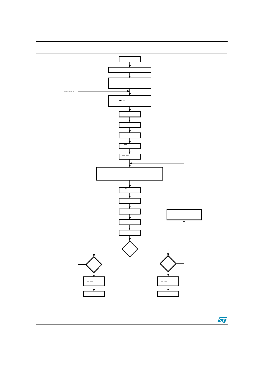
9 Part Numbering
M29W640FT, M29W640FB
68/72
Figure 17. Programmer Equipment Chip Unprotect Flowchart
1. Block Protection Groups are shown in
Appendix A
, Tables
20
and
21
.
PROTECT ALL GROUPS
AI11556
A6, A12, A15 = VIH(1)
E, G, A9 = VID
DATA
W = VIH
E, G = VIH
ADDRESS = CURRENT GROUP ADDRESS
A0, A2, A3 = VIL, A1 =VIH,
A6 =VIL,
A9 = VID,
Others = X
Wait 10ms
=
00h
INCREMENT
CURRENT GROUP
n = 0
CURRENT GROUP = 0
Wait 4
µ
s
W = VIL
++n
= 1000
START
YES
YES
NO
NO
LAST
GROUP
YES
NO
E = VIL
Wait 4
µ
s
G = VIL
Wait 60ns
Read DATA
FAIL
PASS
V
e
r
i
f
y
U
n
p
r
o
t
e
c
t
S
e
t
-
u
p
E
n
d
A9 = VIH
E, G = VIH
A9 = VIH
E, G = VIH
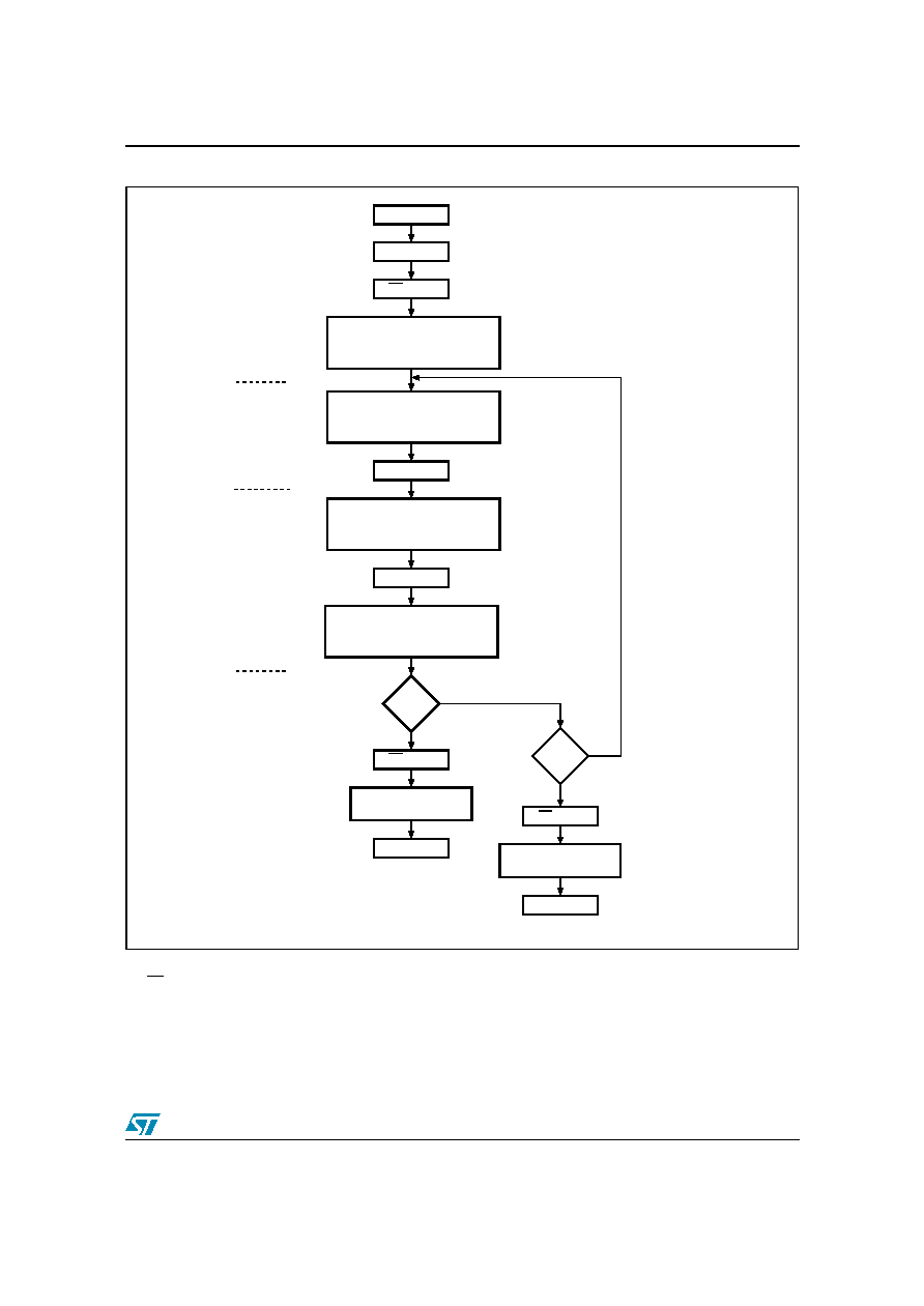
M29W640FT, M29W640FB
9 Part Numbering
69/72
Figure 18. In-System Equipment Group Protect Flowchart
2. Block Protection Groups are shown in
Appendix A
, Tables
20
and
21
.
3. RP can be either at V
IH
or at V
ID
when using the In-System Technique to protect the Extended Block.
AI11563
WRITE 60h
ADDRESS = GROUP ADDRESS
A0, A2, A3, A6 = VIL, A1 = VIH
n = 0
Wait 100
µ
s
WRITE 40h
ADDRESS = GROUP ADDRESS
A0, A2, A3, A6 = VIL, A1 = VIH
RP = VIH
++n
= 25
START
FAIL
PASS
YES
NO
DATA
=
01h
YES
NO
RP = VIH
Wait 4
µ
s
V
e
r
i
f
y
P
r
o
t
e
c
t
S
e
t
-
u
p
E
n
d
READ DATA
ADDRESS = GROUP ADDRESS
A0, A2, A3, A6 = VIL, A1 = VIH
RP = VID
ISSUE READ/RESET
COMMAND
ISSUE READ/RESET
COMMAND
WRITE 60h
ADDRESS = GROUP ADDRESS
A0, A2, A3, A6 = VIL, A1 = VIH
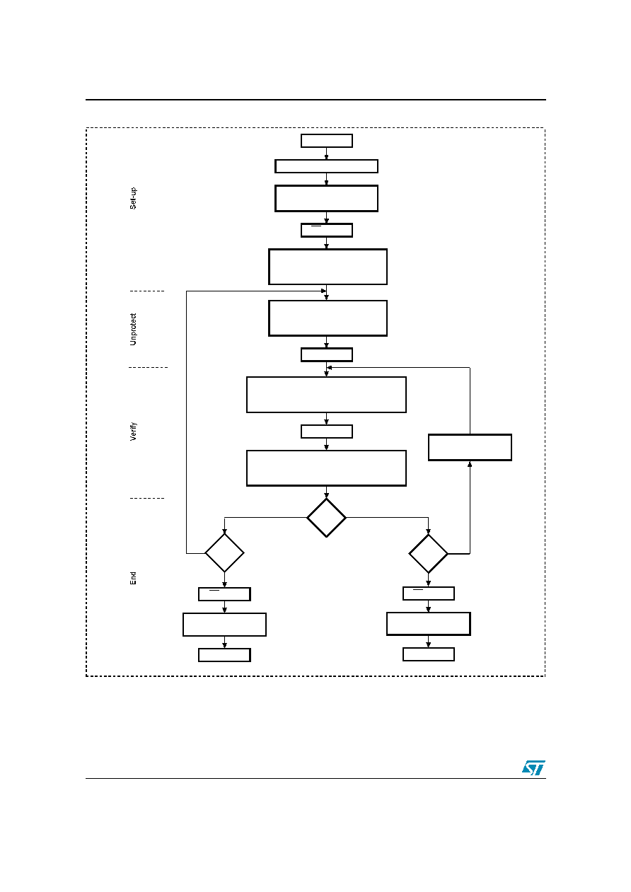
9 Part Numbering
M29W640FT, M29W640FB
70/72
Figure 19. In-System Equipment Chip Unprotect Flowchart
1. Block Protection Groups are shown in
Appendix A
, Tables
20
and
21
.
AI11564
WRITE 60h
ANY ADDRESS WITH
A0, A2, A3 = VIL, A1, A6 = VIH
n = 0
CURRENT GROUP = 0
Wait 10ms
WRITE 40h
ADDRESS = CURRENT GROUP ADDRESS
A0, A2, A3 = VIL, A1, A6 = VIH
RP = VIH
++n
= 1000
START
FAIL
PASS
YES
NO
DATA
=
00h
YES
NO
RP = VIH
Wait 4
µ
s
READ DATA
ADDRESS = CURRENT GROUP ADDRESS
A0, A2, A3 = VIL, A1, A6 = VIH
RP = VID
ISSUE READ/RESET
COMMAND
ISSUE READ/RESET
COMMAND
PROTECT ALL GROUPS
INCREMENT
CURRENT GROUP
LAST
GROUP
YES
NO
WRITE 60h
ANY ADDRESS WITH
A0, A2, A3, A6 = VIL, A1 = VIH
M29W640FT, M29W640FB
10 Revision History
71/72
10 Revision History
Table 30.
Document Revision History
Date
Version
Revision Details
01-Mar-2005
0.1
First Issue.
17-May-2005
0.2
Asynchronous Page mode added.
70ns speed class added.
07-Oct-2005
1.0
Device codes modified.
TFBGA63 replaced by TFBGA48 6x8 package. ECOPACK text updated
Page size changed to 4 Word.
90ns speed class removed.
Quadruple Word/Octuple Byte Program command added.
Table 3: Bus Operations, BYTE = VIL
and
Table 4: Bus Operations, BYTE = VIH
: A0-
A21 addresses for reading the Device Code, the Manufacturer Code, the Extended
Memory Block Verify Code, and the Block Protection Status, have been updated.
Appendix D: Block Protection
:
Table 29: Programmer Technique Bus Operations, BYTE
= VIH or VIL
: A0-A21 addresses updated for Block Protection/Unprotection Verify using
the Programmer technique.
02-Dec-2005
2
Datasheet status changed to
"
Full Datasheet
"
.
60ns speed class added.
Program Suspend and Resume added.
Section 2.8: VPP/Write Protect (VPP/WP)
and
Section 4.2: Fast Program commands
.
Section 4: Command Interface
restructured.
Table 28: Extended Block Address and Data
updated.
15-Dec-2005
3
Double Byte Program commands added in
Section 4: Command Interface
.
Table 3: Bus Operations, BYTE = VIL
and
Table 4: Bus Operations, BYTE = VIH
.: A6
changed from V
IH
to V
IL
for Read Block Protection Status operation.

M29W640FT, M29W640FB
72/72
Information furnished is believed to be accurate and reliable. However, STMicroelectronics assumes no responsibility for the consequences
of use of such information nor for any infringement of patents or other rights of third parties which may result from its use. No license is granted
by implication or otherwise under any patent or patent rights of STMicroelectronics. Specifications mentioned in this publication are subject
to change without notice. This publication supersedes and replaces all information previously supplied. STMicroelectronics products are not
authorized for use as critical components in life support devices or systems without express written approval of STMicroelectronics.
The ST logo is a registered trademark of STMicroelectronics.
All other names are the property of their respective owners
©
2005 STMicroelectronics - All rights reserved
STMicroelectronics group of companies
Australia - Belgium - Brazil - Canada - China - Czech Republic - Finland - France - Germany - Hong Kong - India - Israel - Italy - Japan -
Malaysia - Malta - Morocco - Singapore - Spain - Sweden - Switzerland - United Kingdom - United States of America
www.st.com