 | –≠–ª–µ–∫—Ç—Ä–æ–Ω–Ω—ã–π –∫–æ–º–ø–æ–Ω–µ–Ω—Ç: M3005LD | –°–∫–∞—á–∞—Ç—å:  PDF PDF  ZIP ZIP |
M3005LAB1
M3005LD
REMOTE CONTROL TRANSMITTER
June 1992
1
2
3
4
5
6
7
8
9
10
20
19
18
17
16
15
14
13
12
11
REMO
SEN 6N
SEN 5N
SEN 4N
SEN 3N
SEN 2N
SEN 1N
SEN 0N
ADRM
V
DD
V
SS
DRV 6N
DRV 6N
DRV 6N
DRV 6N
DRV 6N
DRV 6N
DRV 6N
OSC OUT
OSC IN
3005L-01.EPS
PIN CONNECTIONS
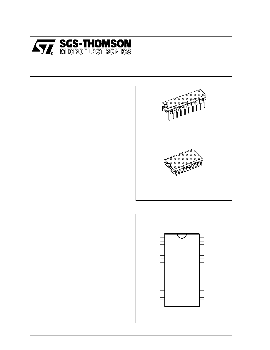
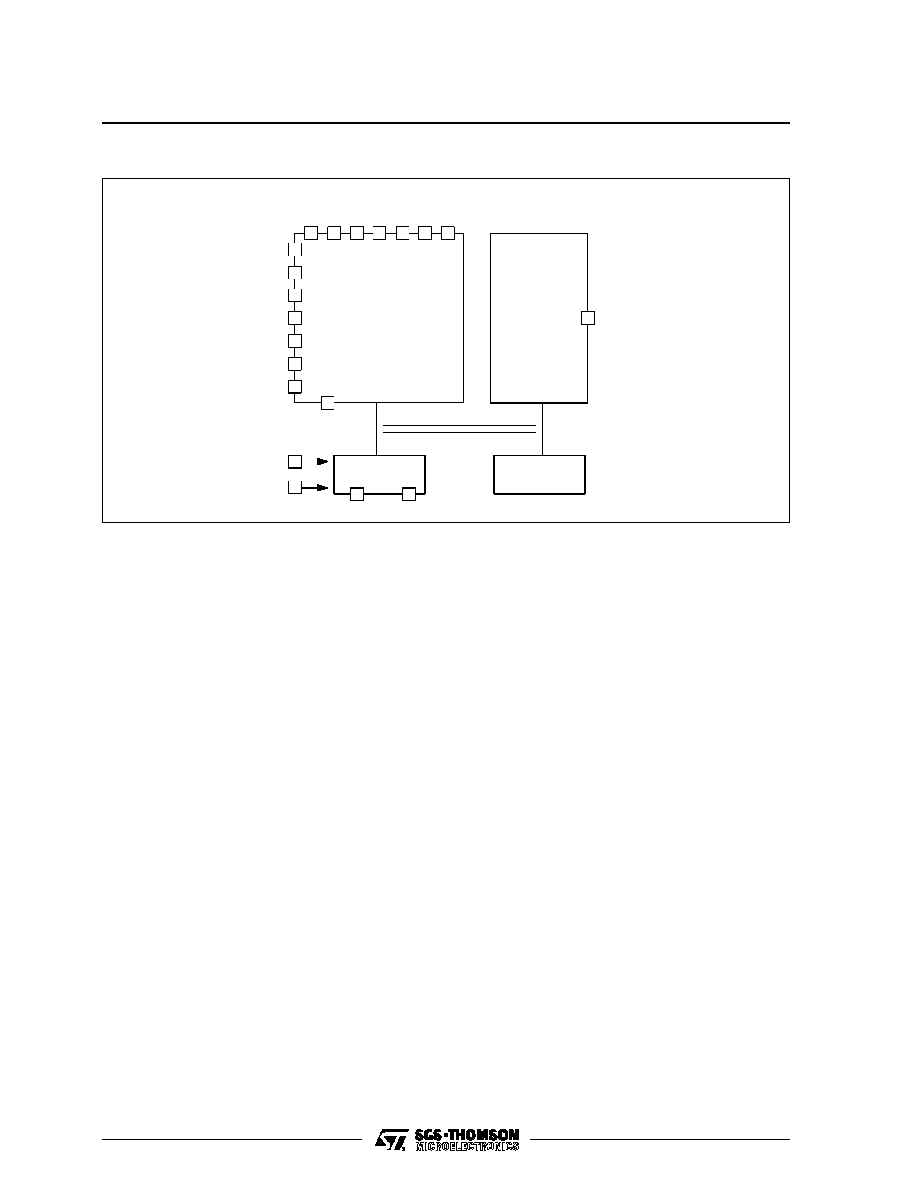
DIP20
(Plastic Package)
ORDER CODE : M3005LAB1
.
FLASHED OR MODULATED TRANSMISSION
.
7 SUB-SYSTEM ADDRESSES
.
UP TO 64 COMMANDS PER SUB-SYSTEM
ADDRESS
.
HIGH-CURRENT
REMOTE
OUTPUT
AT
V
DD
= 6V (≠ I
OH
= 80mA)
.
LOW NUMBER OF ADDITIONAL COMPO-
NENTS
.
KEY RELEASE DETECTION BY TOGGLE
BITS
.
VERY LOW STAND-BY CURRENT (< 2
µ
A)
.
OPERATIONAL CURRENT < 1mA AT 6V
SUPPLY
.
SUPPLY VOLTAGE RANGE 2 TO 6.5V
.
CERAMIC
RESONATOR
CONTROLLED
FREQUENCY (typ. 450kHz)
DESCRIPTION
The M3005LAB1/M3005LD transmitter IC are de-
signed for infrared remote control systems. It has
a total of 448 commands which are divided into 7
sub-system groups with 64 commands each. The
sub-system code may be selected by a press but-
ton, a slider switch or hard wired.
The M3005LAB1/M3005LD generate the pattern
for driving the output stage. These patterns are
pulse distance coded. The pulses are infrared
flashes or modulated. The transmission mode is
defined in conjunction with the sub-system ad-
dress. Modulated pulses allow receivers with nar-
row-band preamplifiers for improved noise
rejection to be used. Flashed pulses require a
wide-band preamplifier within the receiver.
SO20
(Plastic Package)
ORDER CODE : M3005LD
1/10
INPUTS AND OUTPUTS
Key matrix inputs and outputs (DRV0N to
DRV6N and SEN0N to SEN6N)
The transmitter keyboard is arranged as a scanned
matrix. The matrix consists of 7 driver outputs and
7 sense inputs as shown in Figure 1. The driver
outputs DRV0N to DRV6N are open drain N-chan-
nel tran-sistors and they are conductive in the
stand-by mode. The 7 sense inputs (SEN0N to
SEN6N) enable the generation of 56 command
codes. With 2 external diodes all 64 commands are
addressable. The sense inputs have P-channel
pull-up transistors so that they are HIGH until they
are pulled LOW by connecting them to an output
via a key depression to initiate a code transmission.
ADDRESS MODE INPUT (ADRM)
The sub-system address and the transmission
mode are defined by connecting the ADRM input
to one or more driver outputs (DRV0N to DRV6N)
of the key matrix. If more than one driver is con-
nected to ADRM, they must be decoupled by di-
ode s. This allows the defini tion of seven
sub-system addresses as shown in table 3. If driver
DRV6N is connected to ADRM, the data output
format of REMO is modulated or if not connected,
flashed.
The ADRM input has switched pull-up and pull-
down loads. In the stand-by mode only the pull-
down device is active. Whether ADRM is open
(sub-system address 0, flashed mode) or con-
nected to the driver outputs, this input is LOW and
will not cause unwanted dissipation. When the
transmitter becomes active by pressing a key, the
pull-down device is switched off and the pull-up
device is switched on, so that the applied driver
signals are sensed for the decoding of the sub-sys-
tem address and the mode of transmission.
The arrangement of the sub-system address cod-
ing is such that only the driver DRVnM with the
highest number (n) defines the sub-system ad-
dress, e.g. if drivers DRV2N and DRV4N are con-
nected to ADRM, only DRV4N will define the
sub-system address. This option can be used in
systems requiring more than one sub-system ad-
dress. The transmitter may be hard-wired for sub-
system address 2 by connecting DRV1N to ADRM.
If now DRV3N is added to ADRM by a key or a
switch, the transmitted sub-system address
changes to 4. A change of the sub-system address
will not start a transmission.
ADRM
DD
V
V
SS
OSCILLATOR
KEYBOARD
SCAN
PULSE
DISTANCE
MODULATOR
CONTROL
LOGIC
REMO
OUTPUT
OSCI
OSCO
DRV OUTPUTS
S
E
N
I
N
P
U
T
S
0N 1N
3N 4N 5N 6N
2N
0N
1N
2N
3N
4N
5N
6N
3005L-02.EPS
BLOCK DIAGRAM
M3005LAB1 - M3005LD
2/10

REMOTE CONTROL SIGNAL OUTPUT (REMO)
The REMO signal output stage is a push-pull type.
In the HIGH state, a bipolar emitter-follower allows
a high output current. The timing of the data output
format is listed in tables 1 and 2. The information is
defined by the distance t
b
between the leading
edges of the flashed pulses or the first edge of the
modulated pulses (see Figure 3). The format of the
output data is given in Figures 2 and 3. The data
word starts with two toggle bits T1 and T0, followed
by three bits for defining the sub-system address
S2, S1 and S0, and six bits F, E, D, C, B and A which
are defined by the selected key.
In the modulated transmission mode the first toggle
bit is replaced by a constant reference time bit
(REF). This can be used as a reference time for the
decoding sequence. The toggle bits function is an
indication for the decoder that the next instruction
has to be considered as a new command. The
codes for the sub-system address and the selected
key are given in tables 3 and 4.
The REMO output is protected against "Lock-up",
i.e. the length of an output pulse is limited to < 1ms,
even if the oscillator stops during an output pulse.
This avoids the rapid discharge of the battery that
would otherwise be caused by the continuous ac-
tivation of the LED.
OSCILLATOR INPUT / OUTPUT
(OSCI and OSCO)
The external components must be connected to
these pins when using an oscillator with a ceramic
resonator. The oscillator frequency may vary be-
tween 350kHz and 600kHz as defined by the reso-
nator.
FUNCTIONAL DESCRIPTION
Keyboard operation
In the stand -by mode all drivers (DRV0N to
DRV6N) are on (low impedance to V
SS
). Whenever
a key is pressed, one or more of the sense inputs
(SENnN) are tied to ground. This will start the
power-up sequence. First the oscillator is activated
and after the debounce time t
DB
(see Figure 4) the
output drivers (DRV0N to DRV6N) become active
successively.
Within the first scan cycle the transmission mode,
the applied sub-system address and the selected
command code are sensed and loaded into an
internal data latch.
In contrast to the command code, the sub-system
is sensed only within the first scan cycle. If the
applied sub-system address is changed while the
command key is pressed, the transmitted sub-sys-
tem address is not altered.
In a multiple key stroke sequence (see Figure 5)
the command code is always altered in accordance
with the sensed key.
MULTIPLE KEY-STROKE PROTECTION
The keyboard is protected against multiple key-
strokes. If more than one key is pressed at the
same time, the circuit will not generatea new output
at REMO (see Figure 5). In case of a multiple
key-stroke, the scan repetition rate is increased to
detect the release of a key as soon as possible.
There are two restrictions caused by the special
structure of the keyboard matrix :
- The keys switching to ground (code numbers 7,
15, 23, 31, 39, 47, 55 and 63) and the keys
connectedto SEN5N and SEN6N are not covered
completely by the multiple key protection. If one
sense input is switched to ground, further keys on
the same sense line are ignored, i.e. the com-
mand code corresponding to "key to ground" is
transmitted.
- SEN5N and SEN6N are not protected against
multiple keystroke on the same driver line, be-
cause this condition has been used for the defi-
nition of additional codes (code number 56 to 63).
OUTPUT SEQUENCE (data format)
The output operation will start when the selected
code is found. A burst of pulses, including the
latched address and command codes,is generated
at the output REMO as long as a key is pressed.
The format of the output pulse train is given in
Figures 2 and 3. The operation is terminated by
releasing the key or if more than one key is pressed
at the same time. Once a sequence is started, the
transmitted data words will always be completed
after the key is released.
The toggle bits T0 and T1 are incremented if the
key is released for a minimum time t
REL
(see Fig-
ure 4). The toggle bits remain unchanged within a
multiple key-stroke sequence.
M3005LAB1 - M3005LD
3/10

Flash Mode
Carrier Mode
f
OSC
455kHz
600kHz
t
P
4 x t
OSC
Flashed Pulse Width
t
M
12 x t
OSC
tOSC
Modulation Period
N
8*
Number of Modulation Pulses
T
O
1152 x t
OSC
1536 x tOSC
Basic Unit of Pulse Distance
t
W
55296 x t
OSC
73728 x tOSC
Word Distance
The following number of pulses may be selected by Metal option : N = 8, 12, 16.
Note : The different dividing ratio for T
O
and t
W
between flash mode and carrier mode is obtained by changing the modulo of a particular di-
vider from divide by 3 during flash mode to divide by 4 during carrier mode. This allows the use of a 600kHz ceramic resonator dur-
ing carrier mode to obtain a better noise immunity for the receiver without a significant change in T
O
and t
W
. For first samples, the
correct divider ration is obtained by a metal mask option. For final parts, this is automatically done together with the selection of
flash-/carrier mode.
3005L-02.TBL
Table 2 : Pulse Train Separation (t
b
)
Code
t
b
Logic "0"
2 x T
O
Logic "1"
3 x T
O
Toggle Bit Time
2 x T
O
or 3 x T
O
3005L-03.TBL
Table 3 : Transmission Mode and Sub-system
Adress Selection.
The sub-system address and the transmission
mode are defined by connecting the ADRM input
to one or more driver outputs (DRV0N To DRV6N)
of the key matrix. If more than one driver is con-
nected to ADRM, they must be decoupled by di-
odes.
Mode
Sub-system Address
Driver DRVnN for n =
#
S2
S1
S0
0
1
2
3
4
5
6
F
L
A
S
H
E
D
0
1
2
3
4
5
6
1
0
0
0
0
1
1
1
0
0
1
1
0
0
1
0
1
0
1
0
1
O
X
X
X
X
X
O
X
X
X
X
O
X
X
X
O
X
X
O
X
O
M
O
D
U
L
A
T
E
D
0
1
2
3
4
5
6
1
0
0
0
0
1
1
1
0
0
1
1
0
0
1
0
1
0
1
0
1
O
X
X
X
X
X
O
X
X
X
X
O
X
X
X
O
X
X
O
X
O
O
O
O
O
O
O
O
O= connected to ADRM
blank= not connected to ADRM
X = don't care
3005L-04.TBL
Table 1 : Pulse Train Timing
Mode
T
O
(ms)
t
P
(
µ
s)
t
M
(
µ
s)
t
W
(ms)
Flashed
2.53
8.8
-
121
Modulated
2.53
-
t
OSC
121
3005L-01.TBL
M3005LAB1 - M3005LD
4/10
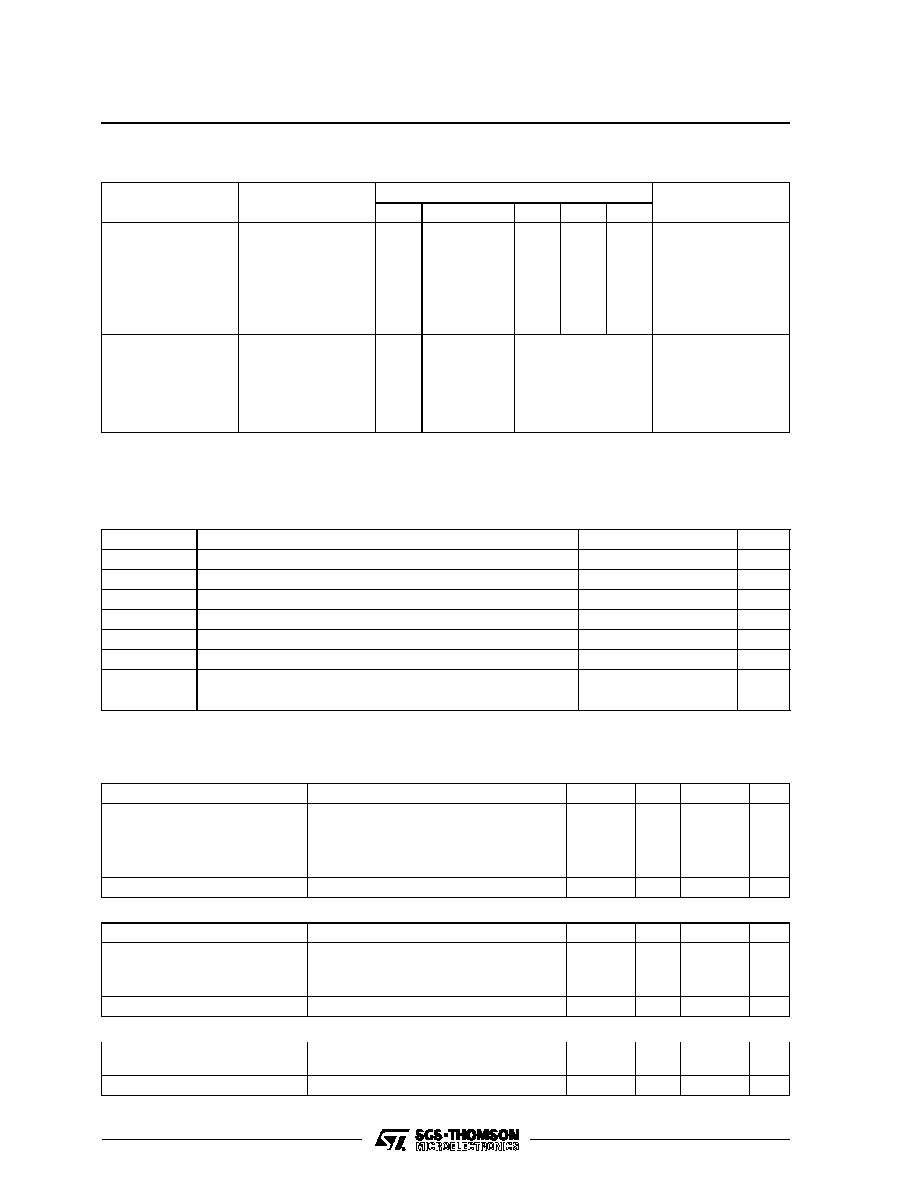
Table 4 : Key Codes
Matrix
Drive
Matrix
Sense
Code
Matrix
Position
F
E
D
C
B
A
DRV0N
DRV1N
DRV2N
DRV3N
DRV4N
DRV5N
DRV6N
V
SS
SEN0N
SEN0N
SEN0N
SEN0N
SEN0N
SEN0N
SEN0N
SEN0N
0
0
0
0
0
0
0
0
0
0
0
0
0
0
0
0
0
0
0
0
0
0
0
0
0
0
0
0
1
1
1
1
0
0
1
1
0
0
1
1
0
1
0
1
0
1
0
1
0
1
2
3
4
5
6
7
*
*
*
*
*
*
*
SEN1N
SEN2N
SEN3N
SEN4N
SEN5N
SEN6N
SEN5N and SEN6N
0
0
0
1
1
1
1
0
1
1
0
0
1
1
1
0
1
0
1
0
1
**
**
**
**
**
*
**
8 to 15
16 to 23
24 to 31
32 to 39
40 to 47
48 to 55
56 to 63
*
The complete matrix drive as shown above for SEN0N is also applicable for the matrix sense inputs SEN1N to SEN6N and the combined
SEN5/SEN6N.
**
The C, B and A codes are identical to SEN0N as given above.
3005L-05.TBL
ABSOLUTE MAXIMUM RATINGS
Symbol
Parameter
Value
Unit
V
DD
Supply Voltage Range
- 0.3 to + 7
V
V
I
Input Voltage Range
- 0.3 to (V
DD
+ 0.3)
V
V
O
Output Voltage Range
- 0.3 to (V
DD
+ 0.3)
V
±
I
D.C. Current into Any Input or Output
Max. 10
mA
- I (REMO) M
Peak REMO Output Current during 10
µ
s, Duty Factor = 1%
Max. 300
mA
P
tot
Power Dissipation per Package for T
A
= - 20 to + 70
o
C
Max. 200
mW
T
stg
Storage Temperature Range
- 55 to + 150
o
C
T
A
Operating Ambient Temperature Range
- 20 to + 70
o
C
3005L-06.TBL
ELECTRICAL CHARACTERISTICS
V
SS
= 0V, T
A
= 25
o
C (unless otherwise specified)
Symbol
Parameter
Test Conditions
Min.
Typ.
Max.
Unit
V
DD
Supply Voltage
T
A
= 0 to + 70
o
C
2
6.5
V
I
DD
Supply Current
∑
Active f
OSC
= 455kHz
V
DD
= 3V
REMO,Output unload
V
DD
= 6V
0.25
1.0
0.5
2
mA
mA
∑
Inactive (stand-by mode)
V
DD
= 6V
2
µ
A
f
OSC
Oscill. Frequency
V
DD
= 2 to 6.5V (cer resonator)
350
600
kHz
KEYBOARD MATRIX - Inputs SE0N to SEN6N
V
IL
Input Voltage Low
V
DD
= 2 to 6.5V
0.3 x V
DD
V
V
IH
Input Voltage High
V
DD
= 2 to 6.5V
0.7 x V
DD
V
- I
I
Input Current
V
DD
= 2V, V
I
= 0V
V
DD
= 6.5V, V
I
= 0V
10
100
100
600
µ
A
µ
A
I
I
Input Leakage Current
V
DD
= 6.5V, V
I
= V
DD
1
µ
A
KEYBOARD MATRIX - Outputs DRV0N to DRV6N
V
OL
Output Voltage "ON"
V
DD
= 2V, I
O
= 0.25mA
V
DD
= 6.5V, I
O
= 2.5mA
0.3
0.6
V
V
I
O
Output Current "OFF"
V
DD
= 6.5V, V
O
= 11V
10
µ
A
3005L-07.TBL
M3005LAB1 - M3005LD
5/10