 | –≠–ª–µ–∫—Ç—Ä–æ–Ω–Ω—ã–π –∫–æ–º–ø–æ–Ω–µ–Ω—Ç: M34116B1 | –°–∫–∞—á–∞—Ç—å:  PDF PDF  ZIP ZIP |
M34116
PCM CONFERENCE CALL
AND TONE GENERATION CIRCUIT
PRELIMINARY DATA
HW AND SW COMPATIBLE WITH M116
1 TO 64 SERIAL CHANNELS PER FRAME
(CONTROLLED BY SYNC SIGNAL PERIOD)
29 MAXIMUM CONFERENCES
1 TO 64 SERIAL CHANNELS PER CONFER-
ENCES
3
SIMULTANEOUS OPERATION MODES
AVAILABLE:
CONFERENCE, TRANSPARENT AND TONE
GENERATION
TYPICAL BIT RATES:
1536/1544/2048/4096Kbits/s
COMPATIBLE WITH ALL KINDS OF PCM
FORMAT
µ
AND A LAW (PIN PROGRAMMABLE)
EQUAL PRIORITY TO EVERY CHANNEL
ONE FRAME AND ONE CHANNEL DELAY
FROM SENDING TO RECEIVING
OVERFLOW INFORMATION FOR EACH CON-
FERENCE BY PIN OS (OVERFLOW SIGNAL-
LING) AND ON DATA BUS ON MPU RE-
QUEST
INSTRUCTION SET COMPATIBLE WITH M3488
PROGRAMMABLE INPUT AND OUTPUT AT-
TENUATION OR GAIN FROM 0 TO 15dB
WITH STEP OF 1dB FOR EACH CHANNEL
TONE
GENERATION
FROM
3.9Hz
TO
3938Hz WITH MIN. STEP OF 3.9Hz
TOTAL OF 7 DIFFERENT TONE OUTPUTS
IN PARALLEL PROGRAMMABLE VIA MPU
(MAXIMUM 4 DIFFERENT FREQUENCIES
AND DURATIONS)
1 MELODY OF MAXIMUM 32 PROGRAMMA-
BLE FREQUENCIES AND DURATIONS
5V POWER SUPPLY
TTL
COMPATIBLE
INPUT
LEVELS,
CMOS/TTL COMPATIBLE OUTPUT LEVELS
MAIN INSTRUCTIONS CONTROLLED BY MI-
CROPROCESSOR INTERFACE:
≠ Channel connection to a conference
≠ Channel attenuation or gain
≠ Channel disconnection from both conference
and transparent modes
≠ Tone and melody generation
≠ Overflow status
≠ Operating mode
≠ Channel status
DESCRIPTION
The M34116 is a product specifically designed for
applications in PCM digital exchanges. It is able
to handle up to 64 channels in any conferences
combination from 1 to 29 conferences in parallel
and to generate seven different tones and one
melody.
The parties in a conference must previously be al-
located through the Digital Switching Matrix
(M3488) in a single serial wire at M34116 PCM
input (IN PCM pin).
The M34116 is full pin and function compatible
with the M116. In addition, it has the capability to
generate tone directly coded in PCM.
For the conference function, each channel is con-
verted inside the chip from PCM law to linear law
(14 bits). Then it is added to its conference, and
the sample of the previous frame is subtracted
from the conference.
In this way a new conference sum signal is gener-
ated.
The channel output signal will contain the infor-
mation of all the other channels in its conference
except its own.
After the PCM encoding, the data is serialized by
the M34116 in the same sequence as the PCM
input frame, with one frame (plus one channel)
delay and will be reallocated by the DSM (M3488)
at the final channel and bus position.
A programmable attenuation or gain can be set
on each channel and for every function: confer-
ence, tone generation and transparent mode.
This is advanced information on a new product now in development or undergoing evaluation. Details are subject to change without notice.
January 1995
DIP24
ORDERING NUMBER: M34116B1
PLCC28
ORDERING NUMBER: M34116C1
1/23
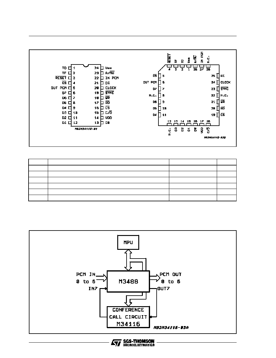
PIN CONNECTIONS (Top view)
ABSOLUTE MAXIMUM RATINGS
Symbol
Parameter
Value
Unit
V
DD
(*)
Supply Voltage
≠ 0.3 to 7
V
V
i
Input Voltage
≠ 0.3 to V
DD
V
O (off)
Off State Output Voltage
≠ 0.3 to 7
V
P
tot
Total Power Dissipation
500
mW
T
stg
Storage Temperature
≠ 65 to 150
∞
C
T
op
Operating Temperature
0 to 70
∞
C
Stresses above those listed under "Absolute Maximum Ratings" may causes permanent damage to the device. This is a stress rating only and
functional operation of the device at these or any other conditions above those indicated in the operational sections of this specification is not
implied. Exposure to absolute maximum rating conditions for extended periods may affect device reliability.
Figure 1: PCM Conference Call Insertion Scheme
DIP24
PLCC28
M34116
2/23
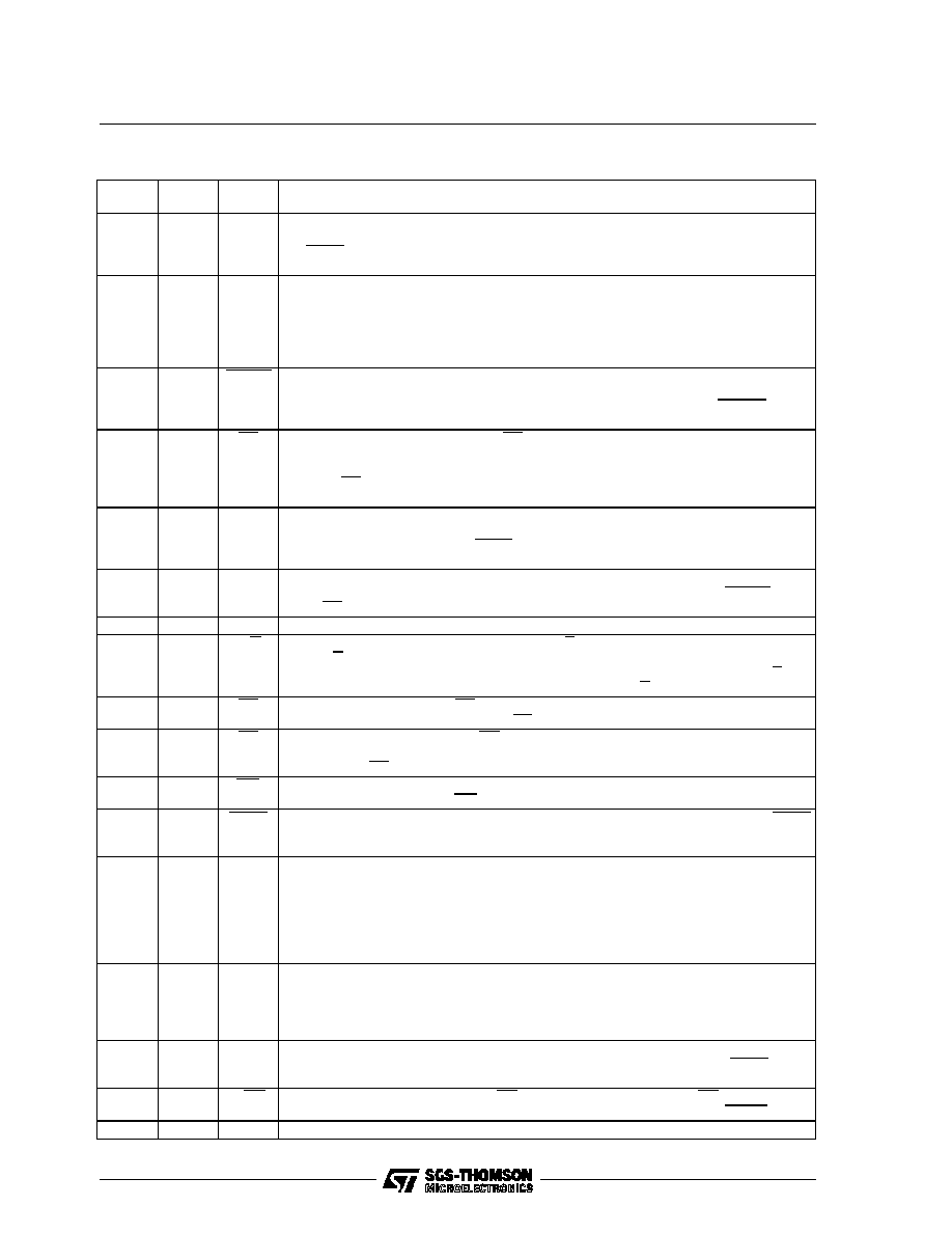
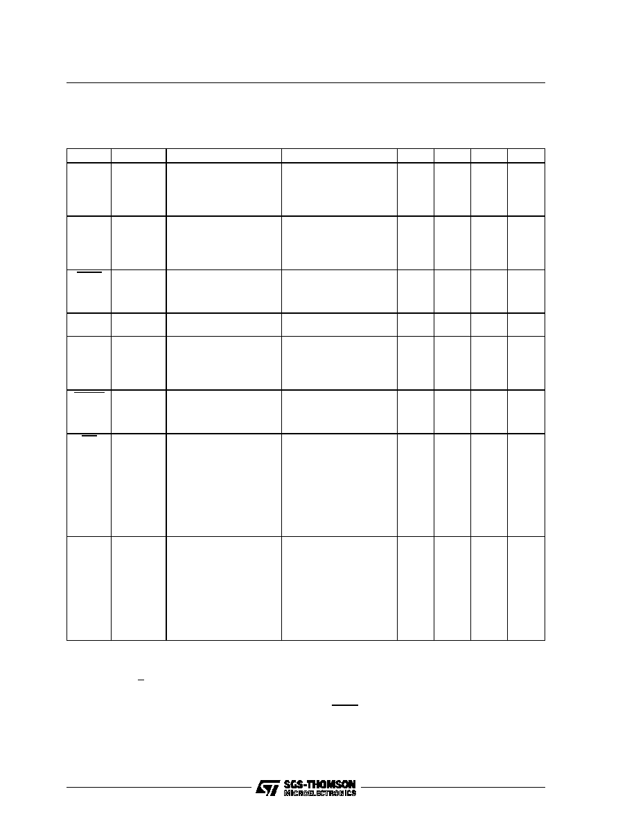
PIN DESCRIPTION
DIP
N
o
PLCC
N
o
Pin
Function
1
2
TD
M116 operating mode only. Tone Duration input pin. When TD = 1, a PCM coded tone
(instead of PCM data) is sent out to all channels enabled by the IT bit. TD is latched by
the SYNC signal so that all channels have the same tone during the same number of
frames. TD = 0 for normal operation.
2
3
TF
M116 operating mode only. Tone Frequency input pin. When TF = 1, the tone amplitude
is high. When TF = 0, the tone amplitude is low. TF is latched by SYNC. The PCM coded
tone level corresponds to 1/10 of the full scale. For M34116 operating mode: Melody
waveform select input pin. When TF = 1, the PCM output of the melody represents a
square wave. When TF = 0, it represents a sine wave. In both cases, the rms level is the
same and is equal to ≠ 6 dBm0 if no attenuation or gain is programmed.
3
4
RESET Master reset input pin. This pin is active low and must be used at the very beginning after
power up to initialize the device or when switching from A law to Mu law. The Internal
initialization routine takes 2 time frames starting from the rising edge of RESET. During
this initialization time, all data bus and PCM output are pulled to a high impedance state.
4
5
OS
Overflow Signalling output pin. When OS = 0 one conference is in overflow. This signal is
anticipated over half time slot with respect to the output channel involved in the conference in
overflow. Example: if output channel 4 is one of the parties of one conference in
overflow, OS = 0 during the second half of the time slot corresponding to output channel 3
and during the first half of the time slot corresponding to output channel 4.
5
6
OUT
PCM
PCM output pin. The bit rate is 4096Kbits/s max. The sign bit is the first bit of the serial
sequence. The first bit of the first channel is found at the rising edge of the CLOCK signal
preceding the rising edge of the SYNC signal. The output buffer is open drain to allow for
multiple connections.
6 to 13
7,
9 to 11,
13 to 16
D0 to
D7
Bidirectional Data bus pins. Data and instructions are transferred to or from the
microprocessor. D0 is the Least Significant Bit. The bus is tristate when RESET is low
and/or CS is high.
14
17
VDD
+5V Supply input. 100nF decoupling capacitor recommended.
15
18
C/D
Control Data input pin. In a write operation C/D = 0 qualifies any bus content as data
while C/D = 1 qualifies it as an opcode. For M116 operating mode only: in a read
operation, the overflow information of the first eight conferences is selected by C/D = 0,
the overflow of the last two conferences and the status by C/D = 1.
16
19
CS
Chip Select input pin. When CS = 0, data and instructions can be transferred to or from
the external microprocessor and when CS = 1 the data bus is in tristate.
17
20
RD
Read control input pin. When RD = 0, read operation is performed. When match
conditions for the opcode exists, data is transferred to the external microprocessor on the
falling edge of RD.
18
21
WR
Write control input pin. Instructions and opcode from the external microprocessor are
latched on the rising edge of WR.
19
23
SYNC
Synchronization input pin. The rising edge of CLOCK preceding the rising edge of SYNC
corresponds to the first bit of the first channel except for PCM frame of 1544Kbits/s. In
this case, it corresponds to the Extra bit (193th).
20
24
CLOCK Master Clock input pin. Typ. operating Frequencies are:
3.072MHz for 24 PCM channels frame (192 bit/frame)
3.088MHz for 24 PCM channels frame with extra bit (193 bit/frame)
4.096MHz for 32 PCM channels frame (256 bit/frame)
8.192MHz for 64 PCM channels frame (512 bit/frame)
Both M34116 an M116 operating modes are possible up to 4.096MHz.
At 8.192MHz only M34116 operating mode is possible.
21
25
EC
External Clock output pin. This pin provides the master clock for the Digital Switching
Matrix (M3488). Normally it is the same signal as applied to the CLOCK input (pin 20).
When the Extra bit is selected with the instruction 5, the first two periods of the master
clock are canceled in order to allow the operation of the M34116 and the DSM with PCM
frame with Extra bit (e.g. 193 bit/frame with PCM I/O of 1544Kbits/s).
22
27
IN PCM PCM input pin. The max bit rate is 4096Kbits/s. The first bit of the first cahnnel is found at
the second rising edge of the CLOCK signal following the rising edge of the SYNC signal.
If Extra bit is selected, then the first bit is shifted by two CLOCK periods.
23
28
A/MU
A Law or MU Law select pin. When A/MU = 1, A Law is selected. When A/MU = 0, MU Law is
selected. The law selection must be done before initializing the device using the RESET pin.
24
1
Vss
Ground.
M34116
3/23
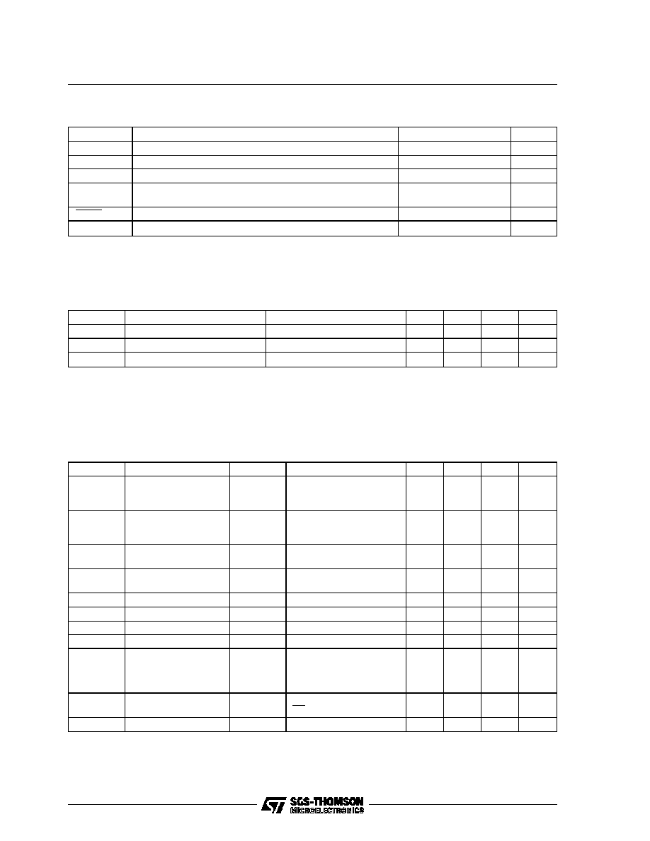
RECOMMENDED OPERATING CONDITIONS
Symbol
Parameter
Value
Unit
V
CC
Supply Voltage
4.75 to 5.25
V
V
i
Input Voltage
0 to 5.25
V
V
O
Off State Output Voltage
0 to 5.25
V
CLOCK Freq.
Input Clock Frequency
3.072/3.088
4.096 / 8.192 (*)
MHz
MHz
SYNC Freq.
Input Synchronization Frequency
8
KHz
T
op
Operating Temperature
0 to 70
∞
C
CAPACITANCES (measurements frequency = 1MHz; 0 to 70
∞
C; unused pins tied to V
SS
)
Symbol
Parameter
Pin (**)
Min.
Typ.
Max.
Unit
C
I
Input Capacitance
1 to 3; 15 to 20; 22 to 23
5
pF
C
I/O
I/O Capacitance
6 to 13
15
pF
C
O
Output Capacitance
4, 5, 21
10
pF
ELECTRICAL CHARACTERISTICS (Tamb = 0 to 70
∞
C, V
CC
= 5V
±
5%)
All DC characteristic are valid 250
µ
s after V
CC
and clock have been applied.
Symbol
Parameter
Pins (**)
Test Condition
Min.
Typ.
Max.
Unit
V
IL
Input Low Level
1 to 3
15 to 20
22 to 23
≠ 0.3
+0.8
V
V
IH
Input High Level
1 to 3
15 to 20
22 to 23
2.0
V
CC
V
V
T≠
Negative Threshold
Voltage
6 to 13 (***)
V
CC
= 5V
0.6
0.9
1.1
V
V
T+
Positive Threshold
Voltage
6 to 13 (***)
V
CC
= 5V
1.5
1.7
2
V
V
HY
Hysteresis
6 to 13 (***)
V
CC
= 5V
0.4
0.8
V
V
OL
Output Low Level
4,6 to 13,21
I
OL
= 2mA
0.4
V
V
OH
Output High Level
4 to 13, 21
I
OH
= 1mA
V
CC
-0.4
V
V
OL
Output Low Level
5
I
OL
= 4.1mA
0.4
V
I
IL
Input Leakage Current
1 to 3
6 to 13
15 to 20
22 to 23
V
IN
= 0 to V
CC
10
µ
A
I
OL
Data Bus Leakage
Current
6 to 13
V
IN
= 0 to V
CC
CS = V
CC
±
10
µ
A
I
CC
Supply Current
14
Clock Freq. = 4.096MHz
50
mA
(*) Only in M34116 Operating Mode.
(**) Pin numbers referred to the DIP24.
(***) Schimitt-trigger inputs.
M34116
4/23
ELECTRICAL CHARACTERISTICS (Tamb = 0 to 70
∞
C, V
CC
= 5V
±
5%)
All DC characteristic are valid 250
µ
s after V
CC
and clock have been applied. C
L
is the max. capacitive
load and R
L
the test pull up resistor.
Signal
Symbol
Parameter
Test Condition
Min.
Typ.
Max.
Unit
CK
Up to
4.096MHz
t
CK
t
WL
t
WH
t
R
t
F
Clock Period
Clock Low Level Width
Clock High Level Width
Rise Time
Fall Time
230
100
100
25
25
ns
ns
ns
ns
ns
CK
8.192MHz
t
CK
t
WL
t
WH
t
R
t
F
Clock Period
Clock Low Level Width
Clock High Level Width
Rise Time
Fall Time
120
50
50
10
10
ns
ns
ns
ns
ns
SYNC
t
SL
t
HL
t
SH
t
WH
Low Level Set-up Time
Low Level Hold Time
High Level Set-up Time
High Level Width
See note 1
30
30
30
t
CK
ns
ns
ns
ns
PCM
Input
t
S
t
H
Set-up Time
Hold Time
35
35
ns
ns
PCM
Output
(Open
drain)
t
PD min.
t
PD max.
Propagation Time Low
Level referred to CK
Propagation Time High
level Referred to CK
C
L
= 50pF R
L
= 1K
40
180
ns
ns
RESET
t
SL
t
HL
t
SH
t
WH
Low Level Set-up Time
Low Level Hold Time
High Level Set-up Time
High Level Width
note 6
50
30
30
t
CK
ns
ns
ns
ns
WR
t
WL
t
WH
t
REP
t
SH
t
HH
t
R
t
F
Low Level Width
High Level Width
Repetition interval
between active pulses.
High Level st-up time to
active read strobe.
High Level hold time to
active read strobe.
Rise Time
Fall Time
note 3 and 4
150
200
500
0
20
60
60
ns
ns
ns
ns
ns
ns
ns
RD
t
WL
t
WH
t
REP
t
SH
t
HH
t
R
t
F
Low Level Width
High Level Width
Repetition interval
between active pulses.
High Level st-up time to
active read strobe.
High Level hold time to
active read strobe.
Rise Time
Fall Time
note 5
180
200
4 t
CK
0
20
60
60
ns
ns
ns
ns
ns
ns
ns
Notes:
1. With Extra Bit operating mode insert this time becomes 3 t
CK
.
2. With Extra Bit operating mode insert these times are 80ns longer.
3. With OPCODE (C/D = I), this time becomes 4tck (6tck if E = 1). E: extra bit indication in "operating mode" instruction.
4. For tone generation instruction, this time becomes 4tck (6tck if E = 1) E: extra bit indication in "operating mode" instruction.
5. With extra bit operating mode insert, this time becomes 6tck.
6. The initialization routine takes 2 frames time starting from the rising edge of RESET - Any access to the device should take place after the
initialization routine is completed. (2 frames time).
M34116
5/23