1/46
November 2001
M36DR432A
M36DR432B
32 Mbit (2Mb x16, Dual Bank, Page) Flash Memory
and 4 Mbit (256K x16) SRAM, Multiple Memory Product
FEATURES SUMMARY
s
SUPPLY VOLTAGE
≠ V
DDF
= V
DDS
=1.65V to 2.2V
≠ V
PPF
= 12V for Fast Program (optional)
s
ACCESS TIME: 100,120ns
s
LOW POWER CONSUMPTION
s
ELECTRONIC SIGNATURE
≠ Manufacturer Code: 20h
≠ Top Device Code, M36DR432A: 00A0h
≠ Bottom Device Code, M36DR432B: 00A1h
FLASH MEMORY
s
32 Mbit (2Mb x16) BOOT BLOCK
≠ Parameter Blocks (Top or Bottom Location)
s
PROGRAMMING TIME
≠ 10µs typical
≠ Double Word Programming Option
s
ASYNCRONOUS PAGE MODE READ
≠ Page width: 4 Word
≠ Page Mode Access Time: 35ns
s
DUAL BANK OPERATION
≠ Read within one Bank while Program or
Erase within the other
≠ No Delay between Read and Write
Operations
s
BLOCK PROTECTION ON ALL BLOCKS
≠ WPF for Block Locking
s
COMMON FLASH INTERFACE
≠ 64 bit Security Code
SRAM
s
4 Mbit (256K x 16 bit)
s
LOW V
DDS
DATA RETENTION: 1V
s
POWER DOWN FEATURES USING TWO
CHIP ENABLE INPUTS
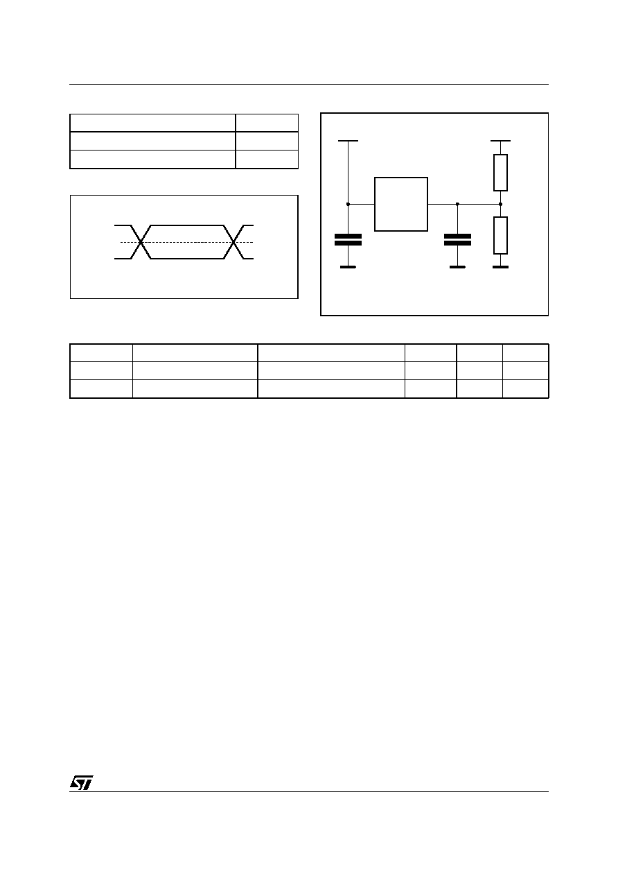
Figure 1. Packages
FBGA
Stacked LFBGA66 (ZA)
8 x 8 ball array

M36DR432A, M36DR432B
2/46
DESCRIPTION
The M36DR432 is a multichip memory device con-
taining a 32 Mbit boot block Flash memory and a
4 Mbit of SRAM. The device is offered in a Stacked
LFBGA66 (0.8 mm pitch) package.
The two components are distinguished by use with
three chip enable inputs: EF for the Flash memory
and, E1S and E2S for the SRAM. The two compo-
nents are also separately power supplied and
grounded.
Figure 2. Logic Diagram
Table 1. Signal Names
AI90203
21
A0-A20
EF
DQ0-DQ15
M36DR432A
M36DR432B
GF
VSSF
16
WF
RPF
WPF
E1S
E2S
GS
WS
UBS
LBS
VSSS
VDDF VPPF VDDS
A0-A17
Address Inputs
A18-A20
Address Inputs for Flash Chip only
DQ0-DQ15
Data Input/Output
V
DDF
Flash Power Supply
V
PPF
Flash Optional Supply Voltage for Fast
Program & Erase
V
SSF
Flash Ground
V
DDS
SRAM Power Supply
V
SSS
SRAM Ground
NC
Not Connected Internally
Flash control functions
EF
Chip Enable input
GF
Output Enable input
WF
Write Enable input
RPF
Reset input
WPF
Write Protect input
SRAM control functions
E1S, E2S
Chip Enable input
GS
Output Enable input
WS
Write Enable input
UBS
Upper Byte Enable input
LBS
Lower Byte Enable input

3/46
M36DR432A, M36DR432B
Figure 3. LFBGA Connections (Top view through package)
AI90204
A
8
7
6
5
4
3
2
1
E
B
F
A12
A13
A11
A20
NC
NC
E2S
DQ12
VSSS
A2
A3
A6
A7
A18
EF
A0
A4
NC
NC
DQ4
WS
DQ15
A9
A16
DQ6
DQ13
NC
WF
A8
A10
A5
NC
VSSF
A17
RPF
A15
A14
NC
NC
VDDF
E1S
A1
NC
NC
GF
VDDS
DQ7
DQ5
DQ14
NC
VSSF
NC
#4
#3
C
DQ10
DQ11
A19
WPF
VPPF
DQ3
DQ2
D
DQ8
DQ9
GS
LBS
UBS
DQ1
DQ0
G
H
#2
#1

M36DR432A, M36DR432B
4/46
Table 2. Absolute Maximum Ratings
(1)
Note: 1. Except for the rating "Operating Temperature Range", stresses above those listed in the Table "Absolute Maximum Ratings" may
cause permanent damage to the device. These are stress ratings only and operation of the device at these or any other conditions
above those indicated in the Operating sections of this specification is not implied. Exposure to Absolute Maximum Rating condi-
tions for extended periods may affect device reliability. Refer also to the STMicroelectronics SURE Program and other relevant qual-
ity documents.
2. Minimum voltage may undershoot to ≠2V during transition and for less than 20ns.
3. Depends on range.
4. V
DD
= V
DDS
= V
DDF
.
Figure 4. Functional Block Diagram
Symbol
Parameter
Value
Unit
T
A
Ambient Operating Temperature
(3)
≠40 to 85
∞C
T
BIAS
Temperature Under Bias
≠40 to 125
∞C
T
STG
Storage Temperature
≠55 to 150
∞C
V
IO
(2)
Input or Output Voltage
≠0.2 to V
DD
(4)
+ 0.3
V
V
DDF
Flash Chip Supply Voltage
≠0.5 to 2.7
V
V
DDS
SRAM Chip Supply Voltage
≠0.2 to 2.6
V
V
PPF
Program Voltage
≠0.5 to 13.0
V
AI90205
Flash Memory
32 Mbit (x16)
VSSF
EF
GF
WF
RPF
WPF
E1S
E2S
GS
WS
UBS
LBS
DQ0-DQ15
VDDF
VPPF
A18-A20
A0-A17
SRAM
4 Mbit (x16)
VSSS
VDDS

5/46
M36DR432A, M36DR432B
SIGNAL DESCRIPTIONS
See Figure 2 and Table 1.
Address Inputs (A0-A17). Addresses A0 to A17
are common inputs for the Flash chip and the
SRAM chip. The address inputs for the Flash
memory are latched during a write operation on
the falling edge of the Flash Chip Enable (EF) or
Write Enable (WF), while address inputs for the
SRAM array are latched during a write operation
on the falling edge of the SRAM Chip Enable lines
(E1S or E2S) or Write Enable (WS).
Address Inputs (A18-A20). Address A18 to A20
are address inputs for the Flash chip. They are
latched during a write operation on the falling edge
of Flash Chip Enable (EF) or Write Enable (WF).
Data Input/Outputs (DQ0-DQ15). The input is
data to be programmed in the Flash or SRAM
memory array or a command to be written to the
C.I. of the Flash chip. Both are latched on the ris-
ing edge of Flash Chip Enable (EF) or Write En-
able (WF) and, SRAM Chip Enable lines (E1S or
E2S) or Write Enable (WS). The output is data
from the Flash memory or SRAM array, the Elec-
tronic Signature Manufacturer or Device codes or
the Status register Data Polling bit DQ7, the Tog-
gle Bits DQ6 and DQ2, the Error bit DQ5 or the
Erase Timer bit DQ3. Outputs are valid when
Flash Chip Enable (EF) and Output Enable (GF) or
SRAM Chip Enable lines (E1S or E2S) and Output
Enable (GS) are active. The output is high imped-
ance when the both the Flash chip and the SRAM
chip are deselected or the outputs are disabled
and when Reset (RPF) is at a V
IL
.
Flash Chip Enable (EF). The Chip Enable input
for Flash activates the memory control logic, input
buffers, decoders and sense amplifiers. EF at V
IH
deselects the memory and reduces the power con-
sumption to the standby level and output do Hi-Z.
EF can also be used to control writing to the com-
mand register and to the Flash memory array,
while WF remains at V
IL
. It is not allowed to set EF
at V
IL
, E1S at V
IL
and E2S at V
IH
at the same time.
Flash Write Enable (WF). The Write Enable in-
put controls writing to the Command Register of
the Flash chip and Address/Data latches. Data are
latched on the rising edge of WF.
Flash Output Enable (GF). The Output Enable
gates the outputs through the data buffers during
a read operation of the Flash chip. When GF and
WF are High the outputs are High impedance.
Flash Reset/Power Down Input (RPF). The RPF
input provides hardware reset of the memory
(without affecting the Configuration Register sta-
tus), and/or Power Down functions, depending on
the Configuration Register status. Reset/Power
Down of the memory is achieved by pulling RPF to
V
IL
for at least t
PLPH
. When the reset pulse is giv-
en, if the memory is in Read, Erase Suspend Read
or Standby, it will output new valid data in t
PHQ7V1
after the rising edge of RPF. If the memory is in
Erase or Program modes, the operation will be
aborted and the reset recovery will take a maxi-
mum of t
PLQ7V
. The memory will recover from
Power Down (when enabled) in t
PHQ7V2
after the
rising edge of RPF. See Tables 1, 26 and Figure
11.
Flash Write Protect (WPF). Write Protect is an
input to protect or unprotect the two lockable pa-
rameter blocks of the Flash memory. When WPF
is at V
IL
, the lockable blocks are protected. Pro-
gram or erase operations are not achievable.
When WPF is at V
IH
, the lockable blocks are un-
protected and they can be programmed or erased
(refer to Table 17).
SRAM Chip Enable (E1S, E2S). The Chip En-
able inputs for SRAM activate the memory control
logic, input buffers and decoders. E1S at V
IH
or
E2S at V
IL
deselects the memory and reduces the
power consumption to the standby level. E1S and
E2S can also be used to control writing to the
SRAM memory array, while WS remains at V
IL
. It
is not allowed to set EF at V
IL
, E1S at V
IL
and E2S
at V
IH
at the same time.
SRAM Write Enable (WS). The Write Enable in-
put controls writing to the SRAM memory array.
WS is active low.
SRAM Output Enable (GS). The Output Enable
gates the outputs through the data buffers during
a read operation of the SRAM chip. GS is active
low.
SRAM Upper Byte Enable (UBS). Enable
the
upper bytes for SRAM (DQ8-DQ15). UBS is active
low.
SRAM Lower Byte Enable (LBS). Enable
the
lower bytes for SRAM (DQ0-DQ7). LBS is active
low.
V
DDF
Supply Voltage (1.65V to 2.2V). Flash memo-
ry power supply for all operations (Read, Program and
Erase).
V
PPF
Programming Voltage (11.4V to 12.6V).
Used to provide high voltage for fast factory pro-
gramming. High voltage on V
PPF
pin is required to
use the Double Word Program instruction. It is
also possible to perform word program or erase in-
structions with V
PPF
pin grounded.
V
DDS
Supply Voltage (1.65V to 2.2V). SRAM
power supply for all operations (Read, Program).
V
SSF
and V
SSS
Ground. V
SSF
and V
SSS
are the
reference for all voltage measurements respec-
tively in the Flash and SRAM chips.
M36DR432A, M36DR432B
6/46
Table 3. Main Operation Modes
Note: X = V
IL
or V
IH
, V
PPFH
= 12V ± 5%.
1. If UBS and LBS are tied together the bus is at 16 bit. For an 8 bit bus configuration use UBS and LBS separately.
Operation
Mode
EF
GF
WF
RPF
WPF
V
PPF
E1S
E2S
GS
WS
UBS, LBS
(1)
DQ15-DQ0
Fla
sh
Me
mory
Read
V
IL
V
IL
V
IH
V
IH
X
Don't care
SRAM must be disabled
Data
Output
Write
V
IL
V
IH
V
IL
V
IH
V
IH
V
CCF
or
V
PPFH
SRAM must be disabled
Data Input
Block
Locking
V
IL
X
X
V
IH
V
IL
Don't care
SRAM must be disabled
X
Standby
V
IH
X
X
V
IH
X
Don't care
Any SRAM mode is allowable
Hi-Z
Reset
X
X
X
V
IL
X
Don't care
Any SRAM mode is allowable
Hi-Z
Output
Disable
V
IL
V
IH
V
IH
V
IH
X
Don't care
Any SRAM mode is allowable
Hi-Z
S
RAM
Read
Flash must be disabled
V
IL
V
IH
V
IL
V
IH
V
IL
Data out
Word Read
Write
Flash must be disabled
V
IL
V
IH
V
IH
V
IL
V
IL
Data in
Word Write
Standby/
Power
Down
Any Flash mode is allowable
V
IH
X
X
X
X
Hi-Z
X
V
IL
X
X
X
Hi-Z
X
X
X
X
V
IH
Hi-Z
Data
Retention
Any Flash mode is allowable
V
IH
X
X
X
X
Hi-Z
X
V
IL
X
X
X
Hi-Z
X
X
X
X
V
IH
Hi-Z
Output
Disable
Any Flash mode is allowable
V
IL
V
IH
V
IH
V
IH
X
Hi-Z

7/46
M36DR432A, M36DR432B
FLASH MEMORY COMPONENT
Organization
The Flash Chip is organized as 2Mb x16 bits. A0-
A20 are the address lines, DQ0-DQ15 are the
Data Input/Output. Memory control is provided by
Chip Enable EF, Output Enable GF and Write En-
able WF inputs.
Reset RPF is used to reset all the memory circuitry
and to set the chip in power down mode if this
function is enabled by a proper setting of the Con-
figuration Register. Erase and Program operations
are controlled by an internal Program/Erase Con-
troller (P/E.C.). Status Register data output on
DQ7 provides a Data Polling signal, DQ6 and DQ2
provide Toggle signals and DQ5 provides error bit
to indicate the state of the P/E.C operations.
Memory Blocks
The device features asymmetrically blocked archi-
tecture. The Flash Chip has an array of 71 blocks
and is divided into two banks A and B, providing
Dual Bank operations. While programming or
erasing in Bank A, read operations are possible
into Bank B or vice versa. The memory also fea-
tures an erase suspend allowing to read or pro-
gram in another block within the same bank. Once
suspended the erase can be resumed. The Bank
Size and Sectorization are summarized in Table 4.
Parameter Blocks are located at the top of the
memory address space for the Top version, and at
the bottom for the Bottom version. The memory
maps are shown in Tables 5, 6, 7 and 8.
The Program and Erase operations are managed
automatically by the P/E.C. Block protection
against Program or Erase provides additional data
security. All blocks are protected at Power Up. In-
structions are provided to protect or unprotect any
block in the application. A second register locks
the protection status while WPF is low (see Block
Locking description). The Reset command does
not affect the configuration of unprotected blocks
and the Configuration Register status.
Device Operations
The following operations can be performed using
the appropriate bus cycles: Read Array (Random,
and Page Modes), Write command, Output Dis-
able, Standby, Reset/Power Down and Block
Locking. See Table 9.
Read. Read operations are used to output the
contents of the Memory Array, the Electronic Sig-
nature, the Status Register, the CFI, the Block
Protection Status or the Configuration Register
status. Read operation of the memory array is per-
formed in asynchronous page mode, that provides
fast access time. Data is internally read and stored
in a page buffer. The page has a size of 4 words
and is addressed by A0-A1 address inputs. Read
operations of the Electronic Signature, the Status
Register, the CFI, the Block Protection Status, the
Configuration Register status and the Security
Code are performed as single asynchronous read
cycles (Random Read). Both Chip Enable EF and
Output Enable GF must be at V
IL
in order to read
the output of the memory.
Write. Write operations are used to give Instruc-
tion Commands to the memory or to latch Input
Data to be programmed. A write operation is initi-
ated when Chip Enable EF and Write Enable WF
are at V
IL
with Output Enable GF at V
IH
. Address-
es are latched on the falling edge of WF or EF
whichever occurs last. Commands and Input Data
are latched on the rising edge of WF or EF which-
ever occurs first. Noise pulses of less than 5ns typ-
ical on EF, WF and GF signals do not start a write
cycle.
Dual Bank Operations. The Dual Bank allows to
read data from one bank of memory while a pro-
gram or erase operation is in progress in the other
bank of the memory. Read and Write cycles can
be initiated for simultaneous operations in different
banks without any delay. Status Register during
Program or Erase must be monitored using an ad-
dress within the bank being modified.
Output Disable. The data outputs are high im-
pedance when the Output Enable GF is at V
IH
with
Write Enable WF at V
IH
.
Standby. The memory is in standby when Chip
Enable EF is at V
IH
and the P/E.C. is idle. The
power consumption is reduced to the standby level
and the outputs are high impedance, independent
of the Output Enable GF or Write Enable WF in-
puts.
Automatic Standby. When in Read mode, after
150ns of bus inactivity and when CMOS levels are
driving the addresses, the chip automatically en-
ters a pseudo-standby mode where consumption
is reduced to the CMOS standby value, while out-
puts still drive the bus.
Power Down. The memory is in Power Down
when the Configuration Register is set for Power
Down and RPF is at V
IL
. The power consumption
is reduced to the Power Down level, and Outputs
are in high impedance, independent of the Chip
Enable EF, Output Enable GF or Write Enable WF
inputs.
Block Locking. Any combination of blocks can
be temporarily protected against Program or
Erase by setting the lock register and pulling WPF
to V
IL
(see Block Lock instruction).
M36DR432A, M36DR432B
8/46
Table 4. Bank Size and Sectorization
Table 5. Bank A, Top Boot Block Addresses
M36DR432A
Table 6. Bank B, Top Boot Block Addresses
M36DR432A
Bank Size
Parameter Blocks
Main Blocks
Bank A
4 Mbit
8 blocks of 4 KWord
7 blocks of 32 KWord
Bank B
28 Mbit
-
56 blocks of 32 KWord
#
Size
(KWord)
Address Range
0
4
1FF000h-1FFFFFh
1
4
1FE000h-1FEFFFh
2
4
1FD000h-1FDFFFh
3
4
1FC000h-1FCFFFh
4
4
1FB000h-1FBFFFh
5
4
1FA000h-1FAFFFh
6
4
1F9000h-1F9FFFh
7
4
1F8000h-1F8FFFh
8
32
1F0000h-1F7FFFh
9
32
1E8000h-1EFFFFh
10
32
1E0000h-1E7FFFh
11
32
1D8000h-1DFFFFh
12
32
1D0000h-1D7FFFh
13
32
1C8000h-1CFFFFh
14
32
1C0000h-1C7FFFh
#
Size
(KWord)
Address Range
0
32
1B8000h-1BFFFFh
1
32
1B0000h-1B7FFFh
2
32
1A8000h-1AFFFFh
3
32
1A0000h-1A7FFFh
4
32
198000h-19FFFFh
5
32
190000h-197FFFh
6
32
188000h-18FFFFh
7
32
180000h-187FFFh
8
32
178000h-17FFFFh
9
32
170000h-177FFFh
10
32
168000h-16FFFFh
11
32
160000h-167FFFh
12
32
158000h-15FFFFh
13
32
150000h-157FFFh
14
32
148000h-14FFFFh
15
32
140000h-147FFFh
16
32
138000h-13FFFFh
17
32
130000h-137FFFh
18
32
128000h-12FFFFh
19
32
120000h-127FFFh
20
32
118000h-11FFFFh
21
32
110000h-117FFFh
22
32
108000h-10FFFFh
23
32
100000h-107FFFh
24
32
0F8000h-0FFFFFh
25
32
0F0000h-0F7FFFh
26
32
0E8000h-0EFFFFh
27
32
0E0000h-0E7FFFh
28
32
0D8000h-0DFFFFh
29
32
0D0000h-0D7FFFh
30
32
0C8000h-0CFFFFh
31
32
0C0000h-0C7FFFh
32
32
0B8000h-0BFFFFh
33
32
0B0000h-0B7FFFh
34
32
0A8000h-0AFFFFh
35
32
0A0000h-0A7FFFh
36
32
098000h-09FFFFh
37
32
090000h-097FFFh
38
32
088000h-08FFFFh
39
32
080000h-087FFFh
40
32
078000h-07FFFFh
41
32
070000h-077FFFh
42
32
068000h-06FFFFh
43
32
060000h-067FFFh
44
32
058000h-05FFFFh
45
32
050000h-057FFFh
46
32
048000h-04FFFFh
47
32
040000h-047FFFh
48
32
038000h-03FFFFh
49
32
030000h-037FFFh
50
32
028000h-02FFFFh
51
32
020000h-027FFFh
52
32
018000h-01FFFFh
53
32
010000h-017FFFh
54
32
008000h-00FFFFh
55
32
000000h-007FFFh

9/46
M36DR432A, M36DR432B
Table 7. Bank B, Bottom Boot Block Addresses
M36DR432B
Table 8. Bank A, Bottom Boot Block Addresses
M36DR432B
#
Size
(KWord)
Address Range
55
32
1F8000h-1FFFFFh
54
32
1F0000h-1F7FFFh
53
32
1E8000h-1EFFFFh
52
32
1E0000h-1E7FFFh
51
32
1D8000h-1DFFFFh
50
32
1D0000h-1D7FFFh
49
32
1C8000h-1CFFFFh
48
32
1C0000h-1C7FFFh
47
32
1B8000h-1BFFFFh
46
32
1B0000h-1B7FFFh
45
32
1A8000h-1AFFFFh
44
32
1A0000h-1A7FFFh
43
32
198000h-19FFFFh
42
32
190000h-197FFFh
41
32
188000h-18FFFFh
40
32
180000h-187FFFh
39
32
178000h-17FFFFh
38
32
170000h-177FFFh
37
32
168000h-16FFFFh
36
32
160000h-167FFFh
35
32
158000h-15FFFFh
34
32
150000h-157FFFh
33
32
148000h-14FFFFh
32
32
140000h-147FFFh
31
32
138000h-13FFFFh
30
32
130000h-137FFFh
29
32
128000h-12FFFFh
28
32
120000h-127FFFh
27
32
118000h-11FFFFh
26
32
110000h-117FFFh
25
32
108000h-10FFFFh
24
32
100000h-107FFFh
23
32
0F8000h-0FFFFFh
22
32
0F0000h-0F7FFFh
21
32
0E8000h-0EFFFFh
20
32
0E0000h-0E7FFFh
19
32
0D8000h-0DFFFFh
18
32
0D0000h-0D7FFFh
17
32
0C8000h-0CFFFFh
16
32
0C0000h-0C7FFFh
15
32
0B8000h-0BFFFFh
14
32
0B0000h-0B7FFFh
13
32
0A8000h-0AFFFFh
12
32
0A0000h-0A7FFFh
11
32
098000h-09FFFFh
10
32
090000h-097FFFh
9
32
088000h-08FFFFh
8
32
080000h-087FFFh
7
32
078000h-07FFFFh
6
32
070000h-077FFFh
5
32
068000h-06FFFFh
4
32
060000h-067FFFh
3
32
058000h-05FFFFh
2
32
050000h-057FFFh
1
32
048000h-04FFFFh
0
32
040000h-047FFFh
#
Size
(KWord)
Address Range
14
32
038000h-03FFFFh
13
32
030000h-037FFFh
12
32
028000h-02FFFFh
11
32
020000h-027FFFh
10
32
018000h-01FFFFh
9
32
010000h-017FFFh
8
32
008000h-00FFFFh
7
4
007000h-007FFFh
6
4
006000h-006FFFh
5
4
005000h-005FFFh
4
4
004000h-004FFFh
3
4
003000h-003FFFh
2
4
002000h-002FFFh
1
4
001000h-001FFFh
0
4
000000h-000FFFh
M36DR432A, M36DR432B
10/46
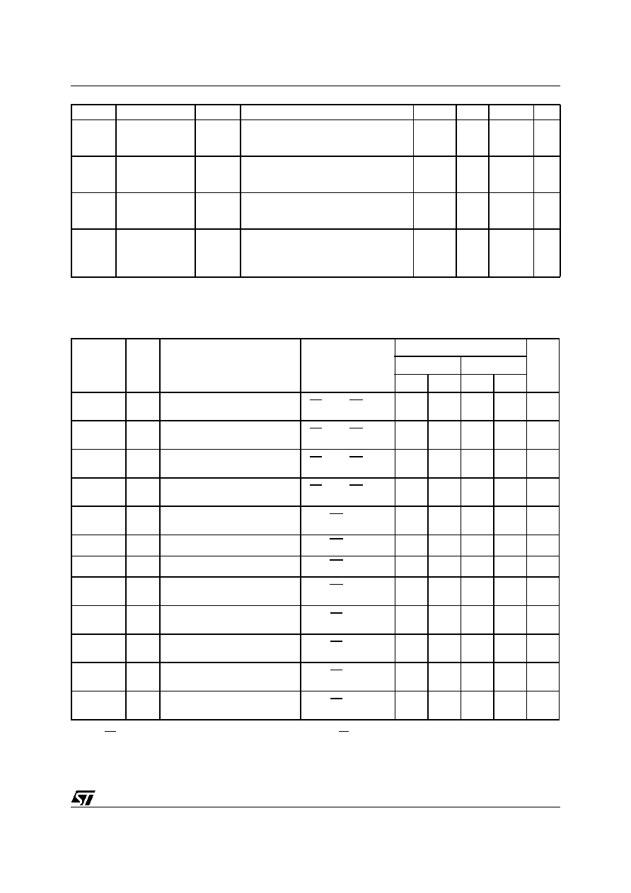
Table 9. User Bus Operations
(1)
Note: 1. X = Don't care.
Table 10. Read Electronic Signature (AS and Read CFI instructions)
Table 11. Read Block Protection (AS and Read CFI instructions)
Table 12. Read Configuration Register (AS and Read CFI instructions)
Operation
EF
GF
WF
RPF
WPF
DQ0-DQ15
Write
V
IL
V
IH
V
IL
V
IH
V
IH
Data Input
Output Disable
V
IL
V
IH
V
IH
V
IH
V
IH
Hi-Z
Standby
V
IH
X
X
V
IH
V
IH
Hi-Z
Reset / Power Down
X
X
X
V
IL
V
IH
Hi-Z
Block Locking
V
IL
X
X
V
IH
V
IL
X
Code
Device
EF
GF
WF
A0
A1
A2-A7
Other
Addresses
DQ0-DQ7
DQ8-DQ15
Manufacturer Code
V
IL
V
IL
V
IH
V
IL
V
IL
0
Don't Care
20h
00h
Device Code
M36DR432A
V
IL
V
IL
V
IH
V
IH
V
IL
0
Don't Care
A0h
00h
M36DR432B
V
IL
V
IL
V
IH
V
IH
V
IL
0
Don't Care
A1h
00h
Block Status
EF
GF
WF
A0
A1
A2-A7
Other
Addresses
A12-A20
DQ0
DQ1
DQ2-DQ15
Protected Block
V
IL
V
IL
V
IH
V
IL
V
IH
0
Don't Care
Block Address
1
0
0000h
Unprotected Block
V
IL
V
IL
V
IH
V
IL
V
IH
0
Don't Care
Block Address
0
0
0000h
Locked Block
V
IL
V
IL
V
IH
V
IL
V
IH
0
Don't Care
Block Address
X
1
0000h
RPF Function
EF
GF
WF
A0
A1
A2-A7
Other Addresses
DQ10
DQ0-DQ9
DQ11-DQ15
Reset
V
IL
V
IL
V
IH
V
IH
V
IH
0
Don't Care
0
Don't Care
Reset/Power Down
V
IL
V
IL
V
IH
V
IH
V
IH
0
Don't Care
1
Don't Care
11/46
M36DR432A, M36DR432B
INSTRUCTIONS AND COMMANDS
Seventeen instructions are defined (see Table
15), and the internal P/E.C. automatically handles
all timing and verification of the Program and
Erase operations. The Status Register Data Poll-
ing, Toggle, Error bits can be read at any time, dur-
ing programming or erase, to monitor the progress
of the operation.
Instructions, made up of one or more commands
written in cycles, can be given to the Program/
Erase Controller through a Command Interface
(C.I.). The C.I. latches commands written to the
memory. Commands are made of address and
data sequences. Two Coded Cycles unlock the
Command Interface. They are followed by an input
command or a confirmation command. The Coded
Sequence consists of writing the data AAh at the
address 555h during the first cycle and the data
55h at the address 2AAh during the second cycle.
Instructions are composed of up to six cycles. The
first two cycles input a Coded Sequence to the
Command Interface which is common to all in-
structions (see Table 15). The third cycle inputs
the instruction set-up command. Subsequent cy-
cles output the addressed data, Electronic Signa-
ture, Block Protection, Configuration Register
Status or CFI Query for Read operations. In order
to give additional data protection, the instructions
for Block Erase and Bank Erase require further
command inputs. For a Program instruction, the
fourth command cycle inputs the address and data
to be programmed. For a Double Word Program-
ming instruction, the fourth and fifth command cy-
cles
input
the
address
and
data
to
be
programmed. For a Block Erase and Bank Erase
instructions, the fourth and fifth cycles input a fur-
ther Coded Sequence before the Erase confirm
command on the sixth cycle. Any combination of
blocks of the same memory bank can be erased.
Erasure of a memory block may be suspended, in
order to read data from another block or to pro-
gram data in another block, and then resumed.
When power is first applied the command interface
is reset to Read Array.
Command sequencing must be followed exactly.
Any invalid combination of commands will reset
the device to Read Array. The increased number
of cycles has been chosen to ensure maximum
data security.
Table 13. Commands
Read/Reset (RD) Instruction. The
Read/Reset
instruction consists of one write cycle giving the
command F0h. It can be optionally preceded by
the two Coded Cycles. Subsequent read opera-
tions will read the memory array addressed and
output the data read.
CFI Query (RCFI) Instruction. Common
Flash
Interface Query mode is entered writing 98h at ad-
dress 55h. The CFI data structure gives informa-
tion on the device, such as the sectorization, the
command set and some electrical specifications.
Table 18, 19, 20 and 21 show the addresses used
to retrieve each data. The CFI data structure con-
tains also a security area; in this section, a 64 bit
unique security number is written, starting at ad-
dress 80h. This area can be accessed only in read
mode by the final user and there are no ways of
changing the code after it has been written by ST.
Write a read instruction (RD) to return to Read
mode.
Auto Select (AS) Instruction. This instruction uses
two Coded Cycles followed by one write cycle giv-
ing the command 90h to address 555h for com-
mand set-up. A subsequent read will output the
Manufacturer or the Device Code (Electronic Sig-
nature), the Block Protection status or the Config-
uration Register status depending on the levels of
A0 and A1 (see Table 10, 11 and 12). A7-A2 must
be at V
IL
, while other address input are ignored.
Hex Code
Command
00h
Bypass Reset
10h
Bank Erase Confirm
20h
Unlock Bypass
30h
Block Erase Resume/Confirm
40h
Double Word Program
60h
Block Protect, or
Block Unprotect, or
Block Lock, or
Write Configuration Register
80h
Set-up Erase
90h
Read Electronic Signature, or
Block Protection Status, or
Configuration Register Status
98h
CFI Query
A0h
Program
B0h
Erase Suspend
F0h
Read Array/Reset

M36DR432A, M36DR432B
12/46
The bank address is don't care for this instruction.
The Electronic Signature can be read from the
memory allowing programming equipment or ap-
plications to automatically match their interface to
the characteristics of Flash Chip. The Manufactur-
er Code is output when the address lines A0 and
A1 are at V
IL
, the Device Code is output when A0
is at V
IH
with A1 at V
IL
.
The codes are output on DQ0-DQ7 with DQ8-
DQ15 at 00h. The AS instruction also allows the
access to the Block Protection Status. After giving
the AS instruction, A0 is set to V
IL
with A1 at V
IH
,
while A12-A20 define the address of the block to
be verified. A read in these conditions will output a
01h if the block is protected and a 00h if the block
is not protected.
The AS Instruction finally allows the access to the
Configuration Register status if both A0 and A1
are set to V
IH
. If DQ10 is '0' only the Reset function
is active as RPF is set to V
IL
(default at power-up).
If DQ10 is '1' both the Reset and the Power Down
functions will be achieved by pulling RPF to V
IL
.
The other bits of the Configuration Register are re-
served and must be ignored. A reset command
puts the device in read array mode.
Write Configuration Register (CR) Instruc-
tion. This instruction uses two Coded Cycles fol-
lowed by one write cycle giving the command 60h
to address 555h. A further write cycle giving the
command 03h writes the contents of address bits
A0-A15 to the 16 bits configuration register. Bits
written by inputs A0-A9 and A11-A15 are reserved
for future use. Address input A10 defines the sta-
tus of the Reset/Power Down functions. It must be
set to V
IL
to enable only the Reset function and to
V
IH
to enable also the Power Down function. At
Power Up all the Configuration Register bits are
reset to '0'.
Enter Bypass Mode (EBY) Instruction. This in-
struction uses the two Coded cycles followed by
one write cycle giving the command 20h to ad-
dress 555h for mode set-up. Once in Bypass
mode, the device will accept the Exit Bypass
(XBY) and Program or Double Word Program in
Bypass mode (PGBY, DPGBY) commands. The
Bypass mode allows to reduce the overall pro-
gramming time when large memory arrays need to
be programmed.
Exit Bypass Mode (XBY) Instruction. This
in-
struction uses two write cycles. The first inputs to
the memory the command 90h and the second in-
puts the Exit Bypass mode confirm (00h). After the
XBY instruction, the device resets to Read Memo-
ry Array mode.
Program in Bypass Mode (PGBY) Instruc-
tion. This instruction uses two write cycles. The
Program command A0h is written to any Address
on the first cycle and the second write cycle latch-
es the Address on the falling edge of WF or EF and
the Data to be written on the rising edge and starts
the P/E.C. Read operations within the same bank
output the Status Register bits after the program-
ming has started. Memory programming is made
only by writing '0' in place of '1'. Status bits DQ6
and DQ7 determine if programming is on-going
and DQ5 allows verification of any possible error.
Program (PG) Instruction. This instruction uses
four write cycles. The Program command A0h is
written to address 555h on the third cycle after two
Coded Cycles. A fourth write operation latches the
Address and the Data to be written and starts the
P/E.C. Read operations within the same bank out-
put the Status Register bits after the programming
has started. Memory programming is made only
by writing '0' in place of '1'. Status bits DQ6 and
DQ7 determine if programming is on-going and
DQ5 allows verification of any possible error. Pro-
gramming at an address not in blocks being
erased is also possible during erase suspend.
Double Word Program (DPG) Instruction. This
feature is offered to improve the programming
throughput, writing a page of two adjacent words
in parallel. High voltage (11.4V to 12.6V) on V
PP
pin is required. This instruction uses five write cy-
cles. The double word program command 40h is
written to address 555h on the third cycle after two
Coded Cycles. A fourth write cycle latches the ad-
dress and data to be written to the first location. A
fifth write cycle latches the new data to be written
to the second location and starts the P/E.C.. Note
that the two locations must have the same address
except for the address bit A0. The Double Word
Program can be executed in Bypass mode (DPG-
BY) to skip the two coded cycles at the beginning
of each command.
Block Protect (BP), Block Unprotect (BU),
Block Lock (BL) Instructions. All blocks are
protected at power-up. Each block of the array has
two levels of protection against program or erase
operation. The first level is set by the Block Protect
instruction; a protected block cannot be pro-
grammed or erased until a Block Unprotect in-
struction is given for that block. A second level of
protection is set by the Block Lock instruction, and
requires the use of the WPF pin, according to the
following scheme:
≠ when WPF is at V
IH
, the Lock status is overrid-
den and all blocks can be protected or unpro-
tected;
≠ when WPF is at V
IL
, Lock status is enabled; the
locked blocks are protected, regardless of their
previous protect state, and protection status
cannot be changed. Blocks that are not locked
can still change their protection status, and pro-
gram or erase accordingly;

13/46
M36DR432A, M36DR432B
≠ the lock status is cleared for all blocks at power
up; once a block has been locked state can be
cleared only with a reset command. The protec-
tion and lock status can be monitored for each
block using the Autoselect (AS) instruction. Pro-
tected blocks will output a `1' on DQ0 and locked
blocks will output a `1' on DQ1.
Refer to Table 14 for a list of the protection states.
Block Erase (BE) Instruction. This
instruction
uses a minimum of six write cycles. The Erase
Set-up command 80h is written to address 555h
on third cycle after the two Coded cycles. The
Block Erase Confirm command 30h is similarly
written on the sixth cycle after another two Coded
cycles and an address within the block to be
erased is given and latched into the memory.
Additional block Erase Confirm commands and
block addresses can be written subsequently to
erase other blocks in parallel, without further Cod-
ed cycles. All blocks must belong to the same
bank of memory; if a new block belonging to the
other bank is given, the operation is aborted. The
erase will start after an erase timeout period of
100µs. Thus, additional Erase Confirm commands
for other blocks must be given within this delay.
The input of a new Erase Confirm command will
restart the timeout period. The status of the inter-
nal timer can be monitored through the level of
DQ3, if DQ3 is '0' the Block Erase Command has
been given and the timeout is running, if DQ3 is '1',
the timeout has expired and the P/E.C. is erasing
the Block(s). If the second command given is not
an erase confirm or if the Coded cycles are wrong,
the instruction aborts, and the device is reset to
Read Array. It is not necessary to program the
block with 00h as the P/E.C. will do this automati-
cally before erasing to FFh. Read operations with-
in the same bank, after the sixth rising edge of WF
or EF, output the status register bits.
During the execution of the erase by the P/E.C.,
the memory accepts only the Erase Suspend ES
instruction; the Read/Reset RD instruction is ac-
cepted during the 100µs time-out period. Data
Polling bit DQ7 returns '0' while the erasure is in
progress and '1' when it has completed. The Tog-
gle bit DQ6 toggles during the erase operation,
and stops when erase is completed.
After completion the Status Register bit DQ5 re-
turns '1' if there has been an erase failure. In such
a situation, the Toggle bit DQ2 can be used to de-
termine which block is not correctly erased. In the
case of erase failure, a Read/Reset RD instruction
is necessary in order to reset the P/E.C.
Bank Erase (BKE) Instruction. This instruction
uses six write cycles and is used to erase all the
blocks belonging to the selected bank. The Erase
Set-up command 80h is written to address 555h
on the third cycle after the two Coded cycles. The
Bank Erase Confirm command 10h is similarly
written on the sixth cycle after another two Coded
cycles at an address within the selected bank. If
the second command given is not an erase con-
firm or if the Coded cycles are wrong, the instruc-
tion aborts and the device is reset to Read Array.
It is not necessary to program the array with 00h
first as the P/E.C. will automatically do this before
erasing it to FFh. Read operations within the same
bank after the sixth rising edge of WF or EF output
the Status Register bits. During the execution of
the erase by the P/E.C., Data Polling bit DQ7 re-
turns '0', then '1' on completion. The Toggle bit
DQ6 toggles during erase operation and stops
when erase is completed. After completion the
Status Register bit DQ5 returns '1' if there has
been an Erase Failure.
Erase Suspend (ES) Instruction. In a dual bank
memory the Erase Suspend instruction is used to
read data within the bank where erase is in
progress. It is also possible to program data in
blocks not being erased.
The Erase Suspend instruction consists of writing
the command B0h without any specific address.
No Coded Cycles are required. Erase suspend is
accepted only during the Block Erase instruction
execution. The Toggle bit DQ6 stops toggling
when the P/E.C. is suspended within 15µs after
the Erase Suspend (ES) command has been writ-
ten. The device will then automatically be set to
Read Memory Array mode. When erase is sus-
pended, a Read from blocks being erased will out-
put DQ2 toggling and DQ6 at '1'. A Read from a
block not being erased returns valid data. During
suspension the memory will respond only to the
Erase Resume ER and the Program PG instruc-
tions. A Program operation can be initiated during
erase suspend in one of the blocks not being
erased. It will result in DQ6 toggling when the data
is being programmed.
Erase Resume (ER) Instruction. If
an
Erase
Suspend instruction was previously executed, the
erase operation may be resumed by giving the
command 30h, at an address within the bank be-
ing erased and without any Coded Cycle.

M36DR432A, M36DR432B
14/46
Table 14. Protection States
(1)
Note: 1. All blocks are protected at power-up, so the default configuration is 001 or 101 according to WPF status.
2. Current state and Next state gives the protection status of a block. The protection status is defined by the write protect pin and by
DQ1 (= 1 for a locked block) and DQ0 (= 1 for a protected block) as read in the Autoselect instruction with A1 = V
IH
and A0 = V
IL
.
3. Next state is the protection status of a block after a Protect or Unprotect or Lock command has been issued or after WPF has
changed its logic value.
4. A WPF transition to V
IH
on a locked block will restore the previous DQ0 value, giving a 111 or 110.
Table 15. Instructions
(1,2)
Current State
(2)
(WP, DQ1, DQ0)
Program/Erase
Allowed
Next State After Event
(3)
Protect
Unprotect
Lock
WP transition
100
yes
101
100
111
000
101
no
101
100
111
001
110
yes
111
110
111
011
111
no
111
110
111
011
000
yes
001
000
011
100
001
no
001
000
011
101
011
no
011
011
011
111 or 110
(4)
Mne.
Instr.
Cyc.
1st Cyc.
2nd Cyc.
3rd Cyc.
4th Cyc.
5th Cyc.
6th Cyc.
RD
(4)
Read/Reset
Memory Array
1+
Addr.
(3)
X
Read Memory Array until a new write cycle is initiated.
Data
F0h
3+
Addr.
555h
2AAh
555h
Read Memory Array until a new
write cycle is initiated.
Data
AAh
55h
F0h
RCFI
CFI Query
1+
Addr.
55h
Read CFI data until a new write cycle is initiated.
Data
98h
AS
(4)
Auto Select
3+
Addr.
555h
2AAh
555h
Read electronic Signature or
Block Protection or Configuration
Register Status until a new cycle
is initiated.
Data
AAh
55h
90h
CR
Configuration
Register Write
4
Addr.
555h
2AAh
555h
Configura-
tion Data
Data
AAh
55h
60h
03h
PG
Program
4
Addr.
555h
2AAh
555h
Program
Address
Read Data Polling or
Toggle Bit until
Program completes.
Data
AAh
55h
A0h
Program
Data
DPG
Double Word
Program
5
Addr.
555h
2AAh
555h
Program
Address 1
Program
Address 2
Note 6, 7
Data
AAh
55h
40h
Program
Data 1
Program
Data 2
EBY
Enter Bypass
Mode
3
Addr.
555h
2AAh
555h
Data
AAh
55h
20h

15/46
M36DR432A, M36DR432B
Note: 1. Commands not interpreted in this table will default to read array mode.
2. For Coded cycles address inputs A11-A20 are don't care.
3. X = Don't Care.
4. The first cycles of the RD or AS instructions are followed by read operations. Any number of read cycles can occur after the com-
mand cycles.
5. During Erase Suspend, Read and Data Program functions are allowed in blocks not being erased.
6. Program Address 1 and Program Address 2 must be consecutive addresses differing only for address bit A0.
7. High voltage on V
PPF
(11.4V to 12.6V) is required for the proper execution of the Double Word Program instruction.
XBY
Exit Bypass
Mode
2
Addr.
X
X
Data
90h
00h
PGBY
Program in
Bypass Mode
2
Addr.
X
Program
Address
Read Data Polling or Toggle Bit until Program
completes.
Data
A0h
Program
Data
DPGBY
Double Word
Program in
Bypass Mode
3
Addr.
X
Program
Address 1
Program
Address 2
Note 6, 7
Data
40h
Program
Data 1
Program
Data 2
BP
Block Protect
4
Addr.
555h
2AAh
555h
Block
Address
Data
AAh
55h
60h
01h
BU
Block Unprotect
1
Addr.
555h
2AAh
555h
Block
Address
Data
AAh
55h
60h
D0h
BL
Block Lock
4
Addr.
555h
2AAh
555h
Block
Address
Data
AAh
55h
60h
2Fh
BE
Block Erase
6+
Addr.
555h
2AAh
555h
555h
2AAh
Block
Address
Data
AAh
55h
80h
AAh
55h
30h
BKE
Bank Erase
6
Addr.
555h
2AAh
555h
555h
2AAh
Bank
Address
Data
AAh
55h
80h
AAh
55h
10h
ES
Erase Suspend
1
Addr.
(3)
X
Read until Toggle stops, then read all the data needed
from any Blocks not being erased then Resume Erase.
Data
B0h
ER
Erase Resume
1
Addr.
Bank
Address
Read Data Polling or Toggle Bits until Erase completes or
Erase is suspended another time
Data
30h
Mne.
Instr.
Cyc.
1st Cyc.
2nd Cyc.
3rd Cyc.
4th Cyc.
5th Cyc.
6th Cyc.
M36DR432A, M36DR432B
16/46
STATUS REGISTER BITS
P/E.C. status is indicated during execution by Data
Polling on DQ7, detection of Toggle on DQ6 and
DQ2, or Error on DQ5 bits. Any read attempt within
the Bank being modified and during Program or
Erase command execution will automatically out-
put these five Status Register bits. The P/E.C. au-
tomatically sets bits DQ2, DQ5, DQ6 and DQ7.
Other bits (DQ0, DQ1 and DQ4) are reserved for
future use and should be masked (see Tables 17
and 16). Read attempts within the bank not being
modified will output array data.
Data Polling Bit (DQ7). When Programming op-
erations are in progress, this bit outputs the com-
plement of the bit being programmed on DQ7. In
case of a double word program operation, the
complement is done on DQ7 of the last word writ-
ten to the command interface, i.e. the data written
in the fifth cycle. During Erase operation, it outputs
a '0'. After completion of the operation, DQ7 will
output the bit last programmed or a '1' after eras-
ing. Data Polling is valid and only effective during
P/E.C. operation, that is after the fourth WF pulse
for programming or after the sixth WF pulse for
erase. It must be performed at the address being
programmed or at an address within the block be-
ing erased. See Figure 25 for the Data Polling
flowchart and Figure 12 for the Data Polling wave-
forms. DQ7 will also flag the Erase Suspend mode
by switching from '0' to '1' at the start of the Erase
Suspend. In order to monitor DQ7 in the Erase
Suspend mode an address within a block being
erased must be provided. For a Read Operation in
Suspend mode, DQ7 will output '1' if the read is at-
tempted on a block being erased and the data val-
ue on other blocks. During Program operation in
Erase Suspend Mode, DQ7 will have the same be-
havior as in the normal program execution outside
of the suspend mode.
Toggle Bit (DQ6). When Programming or Eras-
ing operations are in progress, successive at-
tempts to read DQ6 will output complementary
data. DQ6 will toggle following toggling of either
GF, or EF when GF is at V
IL
. The operation is com-
pleted when two successive reads yield the same
output data. The next read will output the bit last
programmed or a '1' after erasing. The toggle bit
DQ6 is valid only during P/E.C. operations, that is
after the fourth WF pulse for programming or after
the sixth WF pulse for Erase. DQ6 will be set to '1'
if a Read operation is attempted on an Erase Sus-
pend block. When erase is suspended DQ6 will
toggle during programming operations in a block
different from the block in Erase Suspend. Either
EF or GF toggling will cause DQ6 to toggle. See
Figure 25 for Toggle Bit flowchart and Figure 13
for Toggle Bit waveforms.
Toggle Bit (DQ2). This toggle bit, together with
DQ6, can be used to determine the device status
during the Erase operations. During Erase Sus-
pend a read from a block being erased will cause
DQ2 to toggle. A read from a block not being
erased will output data. DQ2 will be set to '1' during
program operation and to `0' in Erase operation.
After erase completion and if the error bit DQ5 is
set to '1', DQ2 will toggle if the faulty block is ad-
dressed.
Error Bit (DQ5). This bit is set to '1' by the P/E.C.
when there is a failure of programming or block
erase, that results in invalid data in the memory
block. In case of an error in block erase or pro-
gram, the block in which the error occurred or to
which the programmed data belongs, must be dis-
carded. Other Blocks may still be used. The error
bit resets after a Read/Reset (RD) instruction. In
case of success of Program or Erase, the error bit
will be set to '0'.
Erase Timer Bit (DQ3). This bit is set to `0' by the
P/E.C. when the last block Erase command has
been entered to the Command Interface and it is
awaiting the Erase start. When the erase timeout
period is finished, DQ3 returns to `1', in the range
of 80µs to 120µs.
Table 16. Polling and Toggle Bits
Mode
DQ7
DQ6
DQ2
Program
DQ7
Toggle
1
Erase
0
Toggle
N/A
Erase Suspend Read
(in Erase Suspend
block)
1
1
Toggle
Erase Suspend Read
(outside Erase Suspend
block)
DQ7
DQ6
DQ2
Erase Suspend Program
DQ7
Toggle
1
17/46
M36DR432A, M36DR432B
Table 17. Status Register Bits
(1)
Note: 1. Logic level '1' is High, '0' is Low. -0-1-0-0-0-1-1-1-0- represent bit value in successive Read operations.
2. In case of double word program DQ7 refers to the last word input.
DQ
Name
Logic Level
Definition
Note
7
Data
Polling
'1'
Erase Complete or erase block
in Erase Suspend.
Indicates the P/E.C. status, check
during Program or Erase, and on
completion before checking bits DQ5
for Program or Erase Success.
'0'
Erase On-going
DQ
Program Complete or data of
non erase block during Erase
Suspend.
DQ
Program On-going
(2)
6
Toggle Bit
'-1-0-1-0-1-0-1-'
Erase or Program On-going
Successive reads output
complementary data on DQ6 while
Programming or Erase operations are
on-going. DQ6 remains at constant
level when P/E.C. operations are
completed or Erase Suspend is
acknowledged.
DQ
Program Complete
'-1-1-1-1-1-1-1-'
Erase Complete or Erase
Suspend on currently addressed
block
5
Error Bit
'1'
Program or Erase Error
This bit is set to '1' in the case of
Programming or Erase failure.
'0'
Program or Erase On-going
4
Reserved
3
Erase Time
Bit
'1'
Erase Timeout Period Expired
P/E.C. Erase operation has started.
Only possible command entry is Erase
Suspend (ES)
'0'
Erase Timeout Period On-going
An additional block to be erased in
parallel can be entered to the P/E.C:
2
Toggle Bit
'-1-0-1-0-1-0-1-'
Erase Suspend read in the
Erase Suspended Block.
Erase Error due to the currently
addressed block (when DQ5 =
'1').
Indicates the erase status and allows
to identify the erased block.
1
Program on-going or Erase
Complete.
DQ
Erase Suspend read on non
Erase Suspend block.
1
Reserved
0
Reserved

M36DR432A, M36DR432B
18/46
POWER CONSUMPTION
Power Down
The memory provides Reset/Power Down control
input RPF. The Power Down function can be acti-
vated only if the relevant Configuration Register bit
is set to '1'. In this case, when the RPF signal is
pulled at V
SS
the supply current drops to typically
I
CC2
(see Table 24), the memory is deselected and
the outputs are in high impedance.If RPF is pulled
to V
SS
during a Program or Erase operation, this
operation is aborted in t
PLQ7V
and the memory
content is no longer valid (see Reset/Power Down
input description).
Power Up
The memory Command Interface is reset on Pow-
er Up to Read Array. Either EF or WF must be tied
to V
IH
during Power Up to allow maximum security
and the possibility to write a command on the first
rising edge of WF.
Supply Rails
Normal precautions must be taken for supply volt-
age decoupling; each device in a system should
have the V
CCF
rails decoupled with a 0.1µF capac-
itor close to the V
CCF
and V
SS
pins. The PCB trace
widths should be sufficient to carry the required
V
CCF
program and erase currents.
19/46
M36DR432A, M36DR432B
COMMON FLASH INTERFACE (CFI)
The Common Flash Interface (CFI) specification is
a JEDEC approved, standardised data structure
that can be read from the Flash memory device.
CFI allows a system software to query the flash
device to determine various electrical and timing
parameters, density information and functions
supported by the device. CFI allows the system to
easily interface to the Flash memory, to learn
about its features and parameters, enabling the
software to configure itself when necessary.
Tables 18, 19, 20, and 21 show the address used
to retrieve each data.
The CFI data structure gives information on the
device, such as the sectorization, the command
set and some electrical specifications. Tables 18,
19, 20, and 21 show the addresses used to re-
trieve each data. The CFI data structure contains
also a security area; in this section, a 64 bit unique
security number is written, starting at address 81h.
This area can be accessed only in read mode and
there are no ways of changing the code after it has
been written by ST. Write a read instruction to re-
turn to Read mode. Refer to the CFI Query instruc-
tion to understand how the M36DR432 enters the
CFI Query mode.
Table 18. Query Structure Overview
Note: The Flash memory display the CFI data structure when CFI Query command is issued. In this table are listed the main sub-sections
detailed in Tables 19, 20 and 21. Query data are always presented on the lowest order data outputs.
Table 19. CFI Query Identification String
Note: 1. Query data are always presented on the lowest - order data outputs (DQ7-DQ0) only. DQ8-DQ15 are `0'.
Offset
Sub-section Name
Description
00h
Reserved
Reserved for algorithm-specific information
10h
CFI Query Identification String
Command set ID and algorithm data offset
1Bh
System Interface Information
Device timing & voltage information
27h
Device Geometry Definition
Flash device layout
P
Primary Algorithm-specific Extended Query table
Additional information specific to the Primary
Algorithm (optional)
A
Alternate Algorithm-specific Extended Query table
Additional information specific to the Alternate
Algorithm (optional)
Offset
Data
Description
00h
0020h
Manufacturer Code
01h
00A0h - top
00A1h - bottom
Device Code
02h-0Fh
reserved
Reserved
10h
0051h
Query Unique ASCII String "QRY"
11h
0052h
Query Unique ASCII String "QRY"
12h
0059h
Query Unique ASCII String "QRY"
13h
0002h
Primary Algorithm Command Set and Control Interface ID code 16 bit ID code
defining a specific algorithm
14h
0000h
15h
offset = P = 0040h
Address for Primary Algorithm extended Query table
16h
0000h
17h
0000h
Alternate Vendor Command Set and Control Interface ID Code second vendor
- specified algorithm supported (note: 0000h means none exists)
18h
0000h
19h
value = A = 0000h
Address for Alternate Algorithm extended Query table
note: 0000h means none exists
1Ah
0000h
M36DR432A, M36DR432B
20/46
Table 20. CFI Query System Interface Information
Offset
Data
Description
1Bh
0017h
V
CCF
Logic Supply Minimum Program/Erase or Write voltage
bit 7 to 4
BCD value in volts
bit 3 to 0
BCD value in 100 millivolts
1Ch
0022h
V
CCF
Logic Supply Maximum Program/Erase or Write voltage
bit 7 to 4
BCD value in volts
bit 3 to 0
BCD value in 100 millivolts
1Dh
0000h
V
PPF
[Programming] Supply Minimum Program/Erase voltage
bit 7 to 4
HEX value in volts
bit 3 to 0
BCD value in 100 millivolts
Note: This value must be 0000h if no V
PP
pin is present
1Eh
00C0h
V
PPF
[Programming] Supply Maximum Program/Erase voltage
bit 7 to 4
HEX value in volts
bit 3 to 0
BCD value in 100 millivolts
Note: This value must be 0000h if no V
PP
pin is present
1Fh
0004h
Typical timeout per single byte/word program (multi-byte program count = 1), 2
n
µs
(if supported; 0000h = not supported)
20h
0000h
Typical timeout for maximum-size multi-byte program or page write, 2
n
µs
(if supported; 0000h = not supported)
21h
000Ah
Typical timeout per individual block erase, 2
n
ms
(if supported; 0000h = not supported)
22h
0000h
Typical timeout for full chip erase, 2
n
ms
(if supported; 0000h = not supported)
23h
0004h
Maximum timeout for byte/word program, 2
n
times typical (offset 1Fh)
(0000h = not supported)
24h
0000h
Maximum timeout for multi-byte program or page write, 2
n
times typical (offset 20h)
(0000h = not supported)
25h
0004h
Maximum timeout per individual block erase, 2
n
times typical (offset 21h)
(0000h = not supported)
26h
0000h
Maximum timeout for chip erase, 2
n
times typical (offset 22h)
(0000h = not supported)
21/46
M36DR432A, M36DR432B
Table 21. Device Geometry Definition
Offset Word
Mode
Data
Description
27h
0016h
Device Size = 2
n
in number of bytes
28h
0001h
Flash Device Interface Code description: Asynchronous x16
29h
0000h
2Ah
0000h
Maximum number of bytes in multi-byte program or page = 2
n
2Bh
0000h
2Ch
0002h
Number of Erase Block Regions within device
bit 7 to 0 = x = number of Erase Block Regions
Note:1. x = 0 means no erase blocking, i.e. the device erases at once in "bulk."
2. x specifies the number of regions within the device containing one or more con-
tiguous Erase Blocks of the same size.
For example, a 128KB device (1Mb)
having blocking of 16KB, 8KB, four 2KB, two 16KB, and one 64KB is considered
to have 5 Erase Block Regions.
Even though two regions both contain 16KB
blocks, the fact that they are not contiguous means they are separate Erase
Block Regions.
3. By definition, symmetrically block devices have only one blocking region.
M36DR432A
M36DR432A
Erase Block Region Information
bit 31 to 16 = z, where the Erase Block(s) within this Region are (z) times 256 bytes in
size. The value z = 0 is used for 128 byte block size.
e.g. for 64KB block size, z = 0100h = 256 => 256 * 256 = 64K
bit 15 to 0 = y, where y+1 = Number of Erase Blocks of identical size within the Erase
Block Region:
e.g.
y = D15-D0 = FFFFh => y+1 = 64K blocks [maximum number]
y = 0 means no blocking (# blocks = y+1 = "1 block")
Note: y = 0 value must be used with number of block regions of one as indicated
by (x) = 0
2Dh
003Eh
2Eh
0000h
2Fh
0000h
30h
0001h
31h
0007h
32h
0000h
33h
0020h
34h
0000h
M36DR432B
M36DR432B
2Dh
0007h
2Eh
0000h
2Fh
0020h
30h
0000h
31h
003Eh
32h
0000h
33h
0000h
34h
0001h

M36DR432A, M36DR432B
22/46
SRAM COMPONENT
Device Operations
The following operations can be performed using
the appropriate bus cycles: Read Array, Write Ar-
ray, Output Disable, Power Down (see Table 3).
Read. Read operations are used to output the
contents of the SRAM Array. The SRAM is in Read
mode whenever Write Enable (WS) is at V
IH
with
Output Enable (GS) at V
IL
, and both Chip Enables
(E1S and E2S) and UBS, LBS combinations are
asserted.
Valid data will be available at the output pins within
t
AVQV
after the last stable address, providing GS is
Low, E1S is Low and E2S is High. If Chip Enable
or Output Enable access times are not met, data
access will be measured from the limiting parame-
ter (t
E1LQV
, t
E2HQV
, or t
GLQV
) rather than the ad-
dress. Data out may be indeterminate at t
E1LQX
,
t
E2HQX
and t
GLQX
, but data lines will always be val-
id at t
AVQV
(see Table 31, Figures 16 and 17).
Write. Write operations are used to write data in
the SRAM. The SRAM is in Write mode whenever
the WS and E1S pins are at V
IL
, with E2S at V
IH
.
Either the Chip Enable inputs (E1S and E2S) or
the Write Enable input (WS) must be de-asserted
during address transitions for subsequent write cy-
cles. Write begins with the concurrence of both
Chip Enables being active with WS at V
IL
. A Write
begins at the latest transition among E1S going to
V
IL
, E2S going to V
IH
and WS going to V
IL
. There-
fore, address setup time is referenced to Write En-
able and both Chip Enables as t
AVWL
, t
AVE1L
and
t
AVE2H
respectively, and is determined by the latter
occurring edge. The Write cycle can be terminated
by the rising edge of E1S, the rising edge of WS or
the falling edge of E2S, whichever occurs first.
If the Output is enabled (E1S=V
IL
, E2S=V
IH
and
GS=V
IL
), then WS will return the outputs to high
impedance within t
WLQZ
of its falling edge. Care
must be taken to avoid bus contention in this type
of operation. Data input must be valid for t
DVWH
before the rising edge of Write Enable, or for
t
DVE1H
before the rising edge of E1S or for t
DVE2L
before the falling edge of E2S, whichever occurs
first, and remain valid for t
WHDX
, t
E1HAX
or t
E2LAX
(see Table 32, Figure 19, 21, 23).
Standby/Power-Down. The SRAM chip has a
Chip Enable power-down feature which invokes
an automatic standby mode (see Table 31, Figure
18) whenever either Chip Enable is de-asserted
(E1S=V
IH
or E2S=V
IL
).
Data Retention
The SRAM data retention performances as V
CCS
go down to V
DR
are described in Table 33 and Fig-
ure 23, 24. In E1S controlled data retention mode,
minimum standby current mode is entered when
E1S
V
CCS
≠ 0.2V
and
E2S
0.2V
or
E2S
V
CCS
≠ 0.2V. In E2S controlled data reten-
tion mode, minimum standby current mode is en-
tered when E2S
0.2V.
Output Disable. The data outputs are high im-
pedance when the Output Enable (GS) is at V
IH
with Write Enable (WS) at V
IH
.
23/46
M36DR432A, M36DR432B
Table 22. AC Measurement Conditions
Figure 5. AC Measurement Waveform
Note: V
DD
means V
DDF
= V
DDS
Figure 6. AC Measurement Load Circuit
Table 23. Device Capacitance
(1)
(T
A
= 25 ∞C, f = 1 MHz)
Note: 1. Sampled only, not 100% tested.
Input Rise and Fall Times
4ns
Input Pulse Voltages
0 to V
DD
Input and Output Timing Ref. Voltages
V
DD
/2
AI90206
VDD
0V
VDD/2
AI90207
CL = 50pF
CL includes JIG capacitance
DEVICE
UNDER
TEST
25k
VDD
25k
VDD
0.1µF
Symbol
Parameter
Test Condition
Min
Max
Unit
C
IN
Input Capacitance
V
IN
= 0V
10
pF
C
OUT
Output Capacitance
V
OUT
= 0V
12
pF
M36DR432A, M36DR432B
24/46
Table 24. DC Characteristics
(T
A
= ≠40 to 85∞C; V
DDF
= V
DDS
= 1.65V to 2.2V)
Symbol
Parameter
Device
Test Condition
Min
Typ
Max
Unit
I
LI
Input Leakage
Current
Flash &
SRAM
0V
V
IN
V
DD
±2
µA
I
LO
Output Leakage
Current
Flash &
SRAM
0V
V
OUT
V
DD
±10
µA
I
DDS
V
DD
Standby
Current
Flash
EF = V
DDF
± 0.2V
V
DDF
= V
DD
max
15
50
µA
SRAM
E1S
V
DDS
≠ 0.2V, E2S
V
DDS
≠ 0.2V,
V
IN
V
DDS
≠ 0.2V
or V
IN
V
DDS
≠ 0.2V, f=0
20
50
µA
I
DDD
Supply Current
(Reset)
Flash
RPF = V
SSF
± 0.2V
2
10
µA
I
DD
Supply Current
SRAM
I
IO
= 0 mA, E1S = V
IL
, E2S = WS = V
IH
,
V
IN
= V
IL
or V
IH
, V
DDS
= V
DD
max,
cycle time = 1µs
10
mA
I
IO
= 0 mA, E1S = V
IL
, E2S = WS = V
IH
,
V
IN
= V
IL
or V
IH
, V
DDS
= V
DD
max,
min cycle time
25
mA
I
DDR
Supply Current
(Read)
Flash
EF = V
IL
, GF
=
V
IH
, f = 5 MHz
10
20
mA
I
DDW
Supply Current
(Program)
Flash
Program in progress
10
20
mA
I
DDWD
Supply Current
(Dual Bank)
Flash
Program/Erase in progress in one bank
Read in the other bank
20
40
mA
I
DDE
Supply Current
(Erase)
Flash
Erase in progress
10
20
mA
I
DDES
(1)
Supply Current
(Erase Suspend)
Flash
Erase Suspend in progress
50
µA
I
DDWS
(1)
Supply Current
(Program
Suspend)
Flash
Program Suspend in progress
50
µA
I
PPS
Program Current
(Standby)
Flash
V
PPF
V
DDS
0.2
5
µA
V
PPF
= 12V ± 0.6V
100
400
µA
I
PPR
Program Current
(Read)
Flash
V
PPF
V
DDS
0.2
5
µA
V
PPF
= 12V ± 0.6V
100
400
µA
I
PPW
Program Current
(Program)
Flash
V
PPF
= 12V ± 0.6V
Program in progress
5
10
mA
I
PPE
Program Current
(Erase)
Flash
V
PPF
= 12V ± 0.6V
Program in progress
5
10
mA
V
IL
Input Low Voltage
Flash &
SRAM
≠0.5
0.4
V
V
IH
Input High
Voltage
Flash &
SRAM
1.4
V
DD
+0.3
V
V
OL
Output Low
Voltage
Flash &
SRAM
V
DDF
= V
DDS
= V
DD
min
I
OL
= 100µA
0.2
V
V
OH
Output High
Voltage
Flash &
SRAM
V
DDF
= V
DDS
= V
DD
min
I
OH
= ≠100µA
V
DD
≠0.1
V
25/46
M36DR432A, M36DR432B
Note: 1.
I
DDES
and
I
DDWS
are specified with device deselected. If device is read while in erase suspend, current draw is sum of
I
DDES
and
I
DDR.
If the device is read while in program suspend, current draw is the sum of
I
DDWS
and
I
DDR
.
Table 25. Flash Read AC Characteristics
(TA = ≠40 to 85∞C; V
DDF
= 1.65V to 2.2V)
Note: 1. Sampled only, not 100% tested.
2. GF may be delayed by up to t
ELQV
- t
GLQV
after the falling edge of EF without increasing t
ELQV
V
PPL
Program Voltage
(Program or
Erase operations)
Flash
1.65
3.6
V
V
PPH
Program Voltage
(Program or
Erase operations)
Flash
11.4
12.6
V
V
PPLK
Program Voltage
(Program and
Erase lock-out)
Flash
1
V
V
LKO
V
DDF
Supply
Voltage (Program
and Erase lock-
out)
Flash
2
V
Symbol
Alt
Parameter
Test Condition
Flash
Unit
100
120
Min
Max
Min
Max
t
AVAV
t
RC
Address Valid to Next Address
Valid
EF = V
IL
, GF = V
IL
100
120
ns
t
AVQV
t
ACC
Address Valid to Output Valid
(Random)
EF = V
IL
, GF = V
IL
100
120
ns
t
AVQV1
t
PAGE
Address Valid to Output Valid
(Page)
EF = V
IL
, GF = V
IL
35
45
ns
t
AXQX
t
OH
Address Transition to Output
Transition
EF = V
IL
, GF = V
IL
0
0
ns
t
EHQX
t
OH
Chip Enable High to Output
Transition
GF = V
IL
0
0
ns
t
EHQZ
(1)
t
HZ
Chip Enable High to Output Hi-Z
GF = V
IL
25
35
ns
t
ELQV
(2)
t
CE
Chip Enable Low to Output Valid
GF = V
IL
100
120
ns
t
ELQX
(1)
t
LZ
Chip Enable Low to Output
Transition
GF = V
IL
0
0
ns
t
GHQX
t
OH
Output Enable High to Output
Transition
EF = V
IL
0
0
ns
t
GHQZ
(1)
t
DF
Output Enable High to Output
Hi-Z
EF = V
IL
25
35
ns
t
GLQV
(2)
t
OE
Output Enable Low to Output
Valid
EF = V
IL
25
35
ns
t
GLQX
(1)
t
OLZ
Output Enable Low to Output
Transition
EF = V
IL
0
0
ns
Symbol
Parameter
Device
Test Condition
Min
Typ
Max
Unit
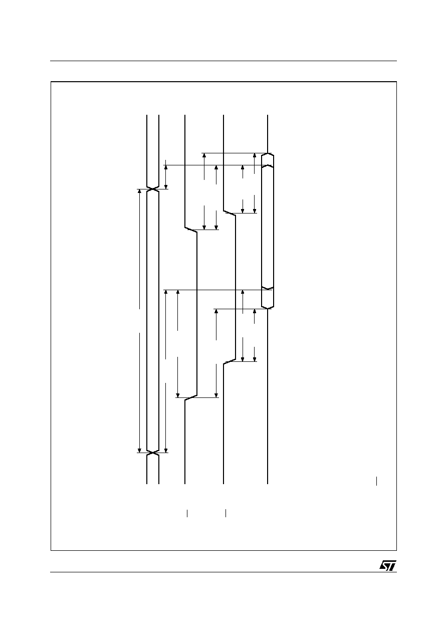
M36DR432A, M36DR432B
26/46
Figure 7. Flash Read AC Waveforms
AI90208
tAVAV
tAVQV
tAXQX
tELQX
tEHQX
tGLQV
tGLQX
tGHQX
VALID
A0-A20
EF
GF
DQ0-DQ15
tELQV
VALID
tEHQZ
tGHQZ
N
o
t
e
:
W
r
i
t
e
E
n
abl
e
(
W
F
)
=
H
i
gh.

27/46
M36DR432A, M36DR432B
Figure 8. Flash Page Read AC Waveforms
AI90209
EF
GF
DQ0-DQ15
A2-A20
VALID
A0-A1
VALID
VALID
tEHQX
tGHQZ
tGHQX
tEHQZ
tELQV
tGLQV
tAVQV
VALID
VALID
VALID
VALID
VALID
VALID
tAVQV1

M36DR432A, M36DR432B
28/46
Table 26. Flash Write AC Characteristics, Write Enable Controlled
(T
A
= ≠40 to 85 ∞C; V
DDF
= 1.65V to 2.2V
Figure 9. Flash Write AC Waveforms, WF Controlled
Note: 1. Address are latched on the falling edge of WF, Data is latched on the rising edge of WF.
Symbol
Alt
Parameter
Flash
Unit
100
120
Min
Max
Min
Max
t
AVAV
t
WC
Address Valid to Next Address Valid
100
120
ns
t
AVWL
t
AS
Address Valid to Write Enable Low
0
0
ns
t
DVWH
t
DS
Input Valid to Write Enable High
50
50
ns
t
ELWL
t
CS
Chip Enable Low to Write Enable Low
0
0
ns
t
GHWL
Output Enable High to Write Enable Low
0
0
ns
t
PLQ7V
RPF Low to Reset Complete During Program/Erase
15
15
µs
t
VDHEL
t
VCS
V
CCF
High to Chip Enable Low
50
50
µs
t
WHDX
t
DH
Write Enable High to Input Transition
0
0
ns
t
WHEH
t
CH
Write Enable High to Chip Enable High
0
0
ns
t
WHGL
t
OEH
Write Enable High to Output Enable Low
30
30
ns
t
WHWL
t
WPH
Write Enable High to Write Enable Low
30
30
ns
t
WLAX
t
AH
Write Enable Low to Address Transition
50
50
ns
t
WLWH
t
WP
Write Enable Low to Write Enable High
50
50
ns
AI90210
EF
GF
WF
A0-A20
DQ0-DQ15
VALID
VALID
VDDF
tVDHEL
tWHEH
tWHWL
tELWL
tAVWL
tWHGL
tWLAX
tWHDX
tAVAV
tDVWH
tWLWH
tGHWL
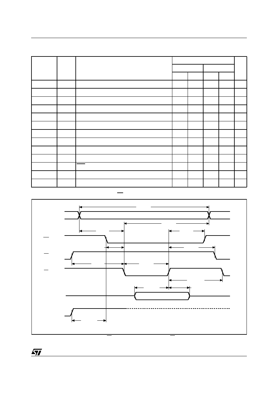
29/46
M36DR432A, M36DR432B
Table 27. Flash Write AC Characteristics, Chip Enable Controlled
(T
A
= ≠40 to 85 ∞C; V
DDF
= 1.65V to 2.2V)
Figure 10. Flash Write AC Waveforms, EF Controlled
Note: Address are latched on the falling edge of EF, Data is latched on the rising edge of EF.
Symbol
Alt
Parameter
Flash
Unit
100
120
Min
Max
Min
Max
t
AVAV
t
WC
Address Valid to Next Address Valid
100
120
ns
t
AVEL
t
AS
Address Valid to Chip Enable Low
0
0
ns
t
DVEH
t
DS
Input Valid to Chip Enable High
50
50
ns
t
EHDX
t
DH
Chip Enable High to Input Transition
0
0
ns
t
EHEL
t
CPH
Chip Enable High to Chip Enable Low
30
30
ns
t
EHGL
t
OEH
Chip Enable High to Output Enable Low
30
30
ns
t
EHWH
t
WH
Chip Enable High to Write Enable High
0
0
ns
t
ELAX
t
AH
Chip Enable Low to Address Transition
50
50
ns
t
ELEH
t
CP
Chip Enable Low to Chip Enable High
50
50
ns
t
GHEL
Output Enable High Chip Enable Low
0
0
ns
t
PLQ7V
RPF Low to Reset Complete During Program/Erase
15
15
µs
t
VDHWL
t
VCS
V
CCF
High to Write Enable Low
50
50
µs
t
WLEL
t
WS
Write Enable Low to Chip Enable Low
0
0
ns
AI90211
EF
GF
WF
A0-A20
DQ0-DQ15
VALID
VALID
VDDF
tVDHWL
tEHWH
tEHEL
tWLEL
tAVEL
tEHGL
tELAX
tEHDX
tAVAV
tDVEH
tELEH
tGHEL
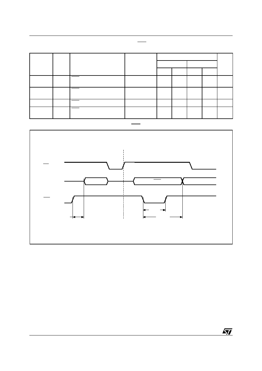
M36DR432A, M36DR432B
30/46
Table 28. Flash Read and Write AC Characteristics, RPF Related
(T
A
= ≠40 to 85∞C; V
DDF
= 1.65V to 2.2V)
Figure 11. Flash Read and Write AC Waveforms, RPF Related
Symbol
Alt
Parameter
Test Condition
Flash
Unit
100
120
Min
Max
Min
Max
t
PHQ7V1
RPF High to Data Valid (Read
Mode)
150
150
ns
t
PHQ7V2
RPF High to Data Valid
(Power Down enabled)
50
50
µs
t
PLPH
t
RP
RPF Pulse Width
100
100
ns
t
PLQ7V
RPF Low to Reset Complete
During Program/Erase
15
15
µs
AI90212
DQ7
WF
RPF
tPLPH
tPHQ7V1,2
VALID
READ
DQ7
VALID
tPLQ7V
PROGRAM / ERASE

31/46
M36DR432A, M36DR432B
Table 29. Flash Program, Erase Times and Program, Erase Endurance Cycles
(T
A
= ≠40 to 85∞C; V
DDF
= 1.65V to 2.2V, V
PPF
= V
DDF
unless otherwise specified)
Note: 1. Max values refer to the maximum time allowed by the internal algorithm before error bit is set. Worst case conditions program or
erase should perform significantly better.
2. Excludes the time needed to execute the sequence for program instruction.
Table 30. Flash Data Polling and Toggle Bits AC Characteristics
(1)
(T
A
= ≠40 to 85 ∞C; V
DDF
= 1.65V to 2.2V)
Note: 1. All other timings are defined in Read AC Characteristics table.
Parameter
Min
Max
(1)
Typ
Typical after
100k W/E Cycles
Unit
Parameter Block (4 KWord) Erase (Preprogrammed)
2.5
0.15
0.4
s
Main Block (32 KWord) Erase (Preprogrammed)
10
1
3
s
Bank Erase (Preprogrammed, Bank A)
2
6
s
Bank Erase (Preprogrammed, Bank B)
10
30
s
Chip Program
(2)
20
25
s
Chip Program (DPG, V
PP
= 12V)
(2)
10
s
Word Program
200
10
10
µs
Program/Erase Cycles (per Block)
100,000
cycles
Symbol
Parameter
Flash
Unit
Min
Max
t
EHQ7V
Chip Enable High to DQ7 Valid (Program, EF Controlled)
10
200
µs
Chip Enable High to DQ7 Valid (Block Erase, EF Controlled)
1
10
s
t
EHQV
Chip Enable High to Output Valid (Program)
10
200
µs
Chip Enable High to Output Valid (Block Erase)
1
10
s
t
Q7VQV
Q7 Valid to Output Valid (Data Polling)
0
ns
t
WHQ7V
Write Enable High to DQ7 Valid (Program, WF Controlled)
10
200
µs
Write Enable High to DQ7 Valid (Block Erase, WF
Controlled)
1
10
s
t
WHQV
Write Enable High to Output Valid (Program)
10
200
µs
Write Enable High to Output Valid (Block Erase)
1
10
s
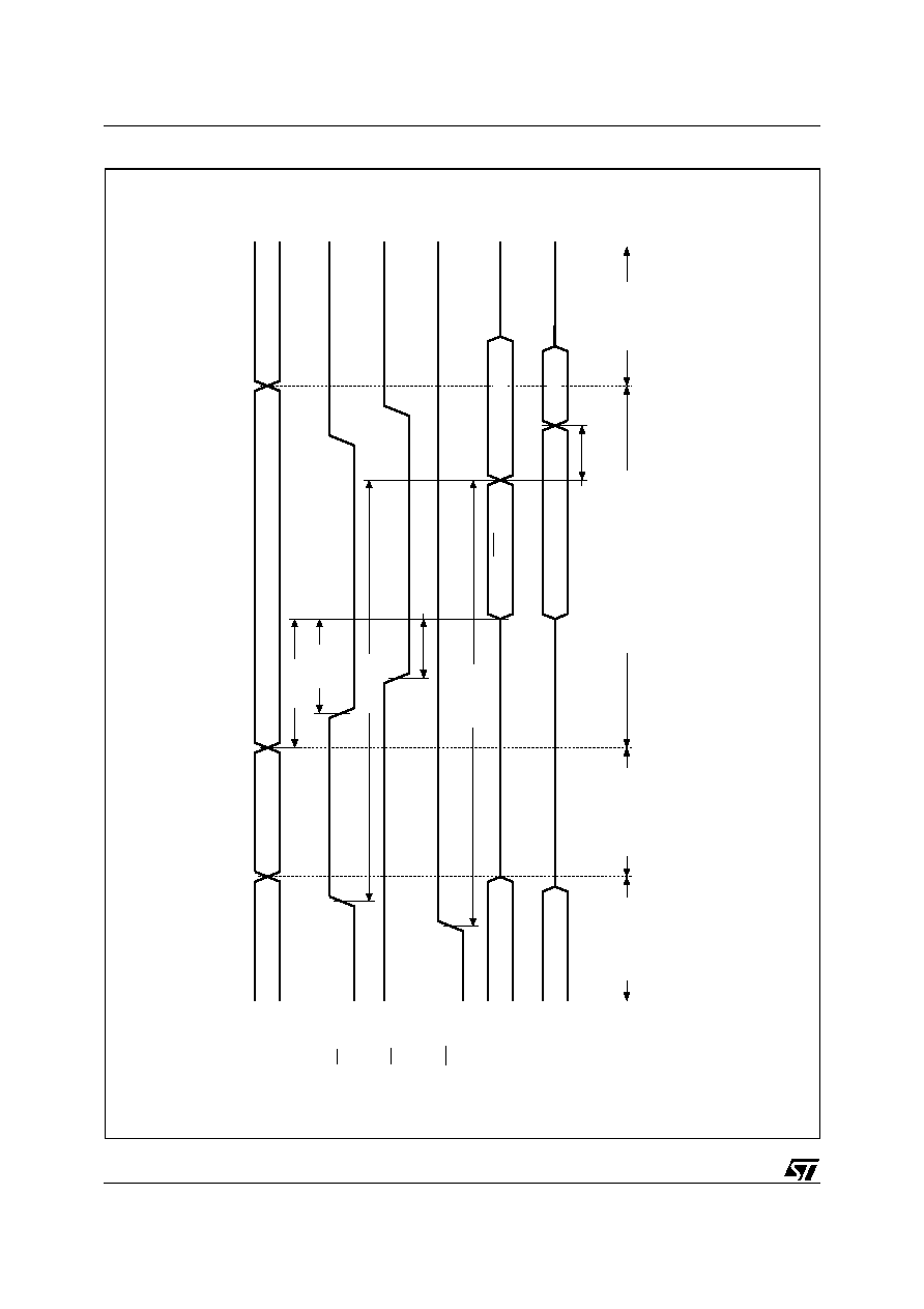
M36DR432A, M36DR432B
32/46
Figure 12. Flash Data Polling DQ7 AC Waveforms
AI90213
EF
GF
WF
A0-A20
DQ7
IGNORE
VALID
DQ0-DQ6/
DQ8-DQ15
ADDRESS (WITHIN BLOCKS)
tAVQV
tEHQ7V
tGLQV
tWHQ7V
VALID
tQ7VQV
DQ7
DATA POLLING (LAST) CYCLE
MEMORY
ARRAY
READ CYCLE
DATA POLLING
READ CYCLES
LAST WRITE
CYCLE OF
PROGRAM
OR ERASE
INSTRUCTION
tELQV

33/46
M36DR432A, M36DR432B
Figure 13. Flash Data Toggle DQ6, DQ2 AC Waveforms
AI90214
EF
GF
WF
A0-A20
DQ6,DQ2
tAVQV
STOP TOGGLE
LAST WRITE
CYCLE OF
PROGRAM
OF ERASE
INSTRUCTION
VALID
VALID
VALID
IGNORE
DATA TOGGLE
READ CYCLE
MEMORY ARRAY
READ CYCLE
tWHQV
tEHQV
tELQV
tGLQV
DATA
TOGGLE
READ CYCLE
DQ0-DQ1,DQ3-DQ5,
DQ7-DQ15
No
t
e
:
A
l
l
ot
he
r
t
i
m
i
n
g
s
a
r
e
a
s
a
no
r
m
al
Re
ad
c
y
c
l
e.
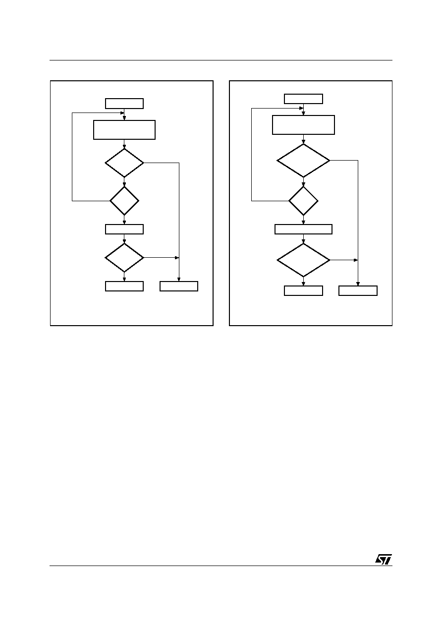
M36DR432A, M36DR432B
34/46
Figure 14. Flash Data Polling Flowchart
Figure 15. Flash Data Toggle Flowchart
READ DQ5 & DQ7
at VALID ADDRESS
START
READ DQ7
FAIL
PASS
AI90215
DQ7
=
DATA
YES
NO
YES
NO
DQ5
= 1
DQ7
=
DATA
YES
NO
READ
DQ5 & DQ6
START
READ DQ6
FAIL
PASS
AI90216
DQ6
=
TOGGLES
NO
NO
YES
YES
DQ5
= 1
NO
YES
DQ6
=
TOGGLES

35/46
M36DR432A, M36DR432B
Table 31. SRAM Read AC Characteristics
(T
A
= ≠40 to 85∞C; V
DDS
= 1.65V to 2.2V)
Note: 1. Sampled only. Not 100% tested.
Figure 16. SRAM Read Mode AC Waveforms, Address Controlled with UBS = LBS = V
IL
Note: E1S = Low, E2S = High, GS = Low, WS = High.
Symbol
Alt
Parameter
SRAM
Unit
Min
Max
t
AVAV
t
RC
Read Cycle Time
100
ns
t
AVQV
t
AA
Address Valid to Output Valid
100
ns
t
AXQX
t
OH
Address Transition to Output Transition
15
ns
t
BHQZ
t
BHZ
UBS, LBS Disable to Hi-Z Output
25
ns
t
BLQV
t
BA
UBS, LBS Access Time
100
ns
t
BLQX
t
BLZ
UBS, LBS Enable to Low-Z Output
5
ns
t
E1HQZ
t
HZ1
Chip Enable 1 High to Output Hi-Z
0
30
ns
t
E1LQV
t
CO1
Chip Enable 1 Low to Output Valid
100
ns
t
E1LQX
t
LZ1
Chip Enable 1 Low to Output Transition
10
ns
t
E2HQV
t
CO2
Chip Enable 2 High to Output Valid
100
ns
t
E2HQX
t
LZ2
Chip Enable 2 High to Output Transition
10
ns
t
E2LQZ
t
HZ2
Chip Enable 2 Low to Output Hi-Z
0
25
ns
t
GHQZ
t
OHZ
Output Enable High to Output Hi-Z
0
30
ns
t
GLQV
t
OE
Output Enable Low to Output Valid
35
ns
t
GLQX
t
OLZ
Output Enable Low to Output Transition
5
ns
t
PD
(1)
Chip Enable 1 High or Chip Enable 2 Low to Power
Down
100
ns
t
PU
(1)
Chip Enable 1 Low or Chip Enable 2 High to Power Up
0
ns
AI90217
tAVAV
tAVQV
tAXQX
A0-A17
DQ0-DQ15
VALID
DATA VALID
DATA VALID
M36DR432A, M36DR432B
36/46
Figure 17. SRAM Read AC Waveforms, E1S, E2S or GS Controlled
Note: Write Enable (WS) = High.
Figure 18. SRAM Standby AC Waveforms
AI90218
tAVAV
tAVQV
tAXQX
tE1LQV
tE1LQX
tE1HQZ
tGLQV
tGLQX
tGHQZ
DATA VALID
A0-A17
E1S
GS
DQ0-DQ15
tE2HQV
tE2HQX
VALID
tE2LQZ
E2S
tBLQV
tBLQX
tBHQZ
UBS, LBS
AI90219
tPD
E2S
IDD
tPU
50%
E1S

37/46
M36DR432A, M36DR432B
Table 32. SRAM Write AC Characteristics
(T
A
= ≠40 to 85∞C; V
DDS
= 1.65V to 2.2V)
Note: 1. t
AS
is measured from the address valid to the beginning of write.
2. t
WR
is measured from the end or write to the address change. t
WR
applied in case a write ends as E1S or WS going high.
3. t
CW
is measured from E1S going low end of write.
4. A Write occurs during the overlap (t
WP
) of low E1S and low WS. A write begins when E1S goes low and WS goes low with asserting
UBS or LBS for single byte operation or simultaneously asserting UBS and LBS for double byte operation. A write ends at the ear-
liest transition when E1S goes high and WS goes high. The t
WP
is measured from the beginning of write to the end of write.
Symbol
Alt
Parameter
SRAM
Unit
Min
Max
t
AVAV
t
WC
Write Cycle Time
100
ns
t
AVE1L
t
AS
(1)
Address Valid to Chip Enable 1 Low
0
ns
t
AVE2H
t
AS
(1)
Address Valid to Chip Enable 2 High
0
ns
t
AVWH
t
AW
Address Valid to Write Enable High
80
ns
t
AVWL
t
AS
(1)
Address Valid to Write Enable Low
0
ns
t
BLWH
t
BW
UBS, LBS Valid to End of Write
80
ns
t
DVE1H
t
DW
Input Valid to Chip Enable 1 High
40
ns
t
DVE2L
t
DW
Input Valid to Chip Enable 2 Low
40
ns
t
DVWH
t
DW
Input Valid to Write Enable High
40
ns
t
E1HAX
t
WR
(2)
Chip Enable 1 High to Address Transition
0
ns
t
E1LWH
,
t
E2HWH
t
CW
(3)
Chip Select to End of Write
80
ns
t
E2LAX
t
WR
(2)
Chip Enable 2 Low to Address Transition
0
ns
t
GHQZ
t
GHZ
Output Enable Higt to Output Hi-Z
25
ns
t
WHAX
t
WR
(2)
Write Enable High to Address Transition
0
ns
t
WHDX
t
DH
Write Enable High to Input Transition
0
ns
t
WHQX
t
OW
Write Enable High to Output Transition
5
ns
t
WLQZ
t
WHZ
Write Enable Low to Output Hi-Z
35
ns
t
WLWH
t
WP
(4)
Write Enable Pulse Width
70
ns

M36DR432A, M36DR432B
38/46
Figure 19. SRAM Write AC Waveforms, WS Controlled with GS Low
Note: Output Enable (GS) = Low.
Figure 20. SRAM Write AC Waveforms, WS Controlled with GS High
AI90220
tAVAV
tWHAX
tDVWH
INPUT VALID
A0-A17
E1S
WS
DQ0-DQ15
VALID
E2S
tAVWH
tAVE2H
tWLWH
tAVWL
tWLQZ
tWHDX
tWHQX
tBLWH
UBS, LBS
tE2HWH
tAVE1L
tE1LWH
AI90221
tAVAV
tWHAX
tDVWH
INPUT VALID
A0-A17
E1S
WS
DQ0-DQ15
VALID
E2S
tAVWH
tAVE2H
tWLWH
tAVWL
tWHDX
tWHQX
tBLWH
UBS, LBS
tE2HWH
tAVE1L
tE1LWH
GS
tGHQZ

39/46
M36DR432A, M36DR432B
Figure 21. SRAM Write Cycle Waveform, UBS and LBS Controlled
Figure 22. SRAM Write AC Waveforms, E1S Controlled
Note: Output Enable (GS) = High.
AI90222
tAVAV
tE1HAX
tDVWH
A0-A17
E1S
WS
DQ0-DQ15
VALID
E2S
tAVWH
tAVWL
tWHDX
DATA VALID
tBLWH
UBS, LBS
tE1LWH
tE2HWH
tWLWH
AI90223
tAVAV
tE1HAX
tDVE1H
A0-A17
E1S
WS
DQ0-DQ15
VALID
E2S
tAVE1L
tAVWL
tWHDX
INPUT VALID
tBLWH
UBS, LBS
tE1LWH
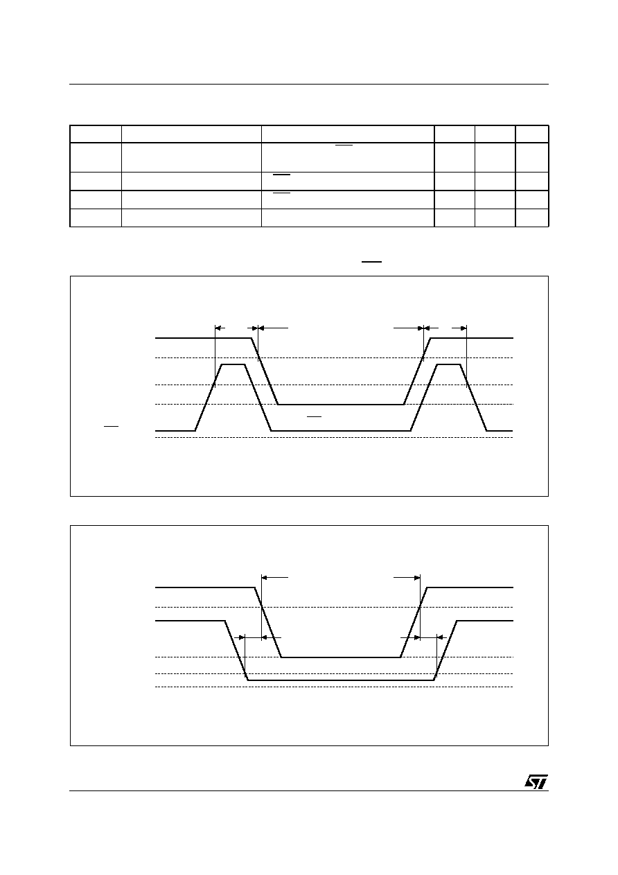
M36DR432A, M36DR432B
40/46
Table 33. SRAM Low V
CCS
Data Retention Characteristics
(1, 2)
(T
A
= ≠40 to 85∞C; V
DDS
= 1.65V to 2.2V)
Note: 1. All other Inputs V
IH
V
DD
≠ 0.2V or V
IL
0.2V.
2. Sampled only. Not 100% tested.
Figure 23. SRAM Low V
DDS
Data Retention AC Waveforms, E1S Controlled
Figure 24. SRAM Low V
DDS
Data Retention AC Waveforms, E2S Controlled
Symbol
Parameter
Test Condition
Min
Max
Unit
I
DDDR
Supply Current (Data Retention)
V
DDS
= 1.2V, E1S
V
DDS
≠ 0.2V,
E2S
V
DDS
≠ 0.2V or E2S
0.2V, f = 0
10
µA
V
DR
Supply Voltage (Data Retention)
E1S
V
DDS
≠ 0.2V, E2S
0.2V, f = 0
1
2.2
V
t
CDR
Chip Disable to Power Down
E1S
V
CCS
≠ 0.2V, E2S
0.2V, f = 0
0
ns
t
R
Operation Recovery Time
t
RC
ns
AI90224
1.65 V
E1S
tCDR
E1S
VDDS ≠ 0.2V
1.2 V
VDR
VSSS
VDDS
tR
DATA RETENTION MODE
AI90225
1.65 V
E2S
tCDR
E2S
0.2V
VDR
VSSS
VDDS
tR
DATA RETENTION MODE
0.4 V

41/46
M36DR432A, M36DR432B
Table 34. Ordering Information Scheme
Devices are shipped from the factory with the memory content bits erased to '1'.
Table 35. Daisy Chain Ordering Scheme
For a list of available options (Speed, Package, etc...) or for further information on any aspect of this de-
vice, please contact the STMicroelectronics Sales Office nearest to you.
Example:
M36DR432A
100 ZA
6
T
Device Type
M36 = MMP (Flash + SRAM)
Architecture
D = Dual Bank, Page Mode
Operating Voltage
R = V
DDF
= V
DDS
=1.65V to 2.2V
SRAM Chip Size & Organization
4 = 4 Mbit (256K x 16 bit)
Device Function
32A = 32 Mbit (x16), Dual Bank: 1/8-7/8 partitioning, Top Boot
32B = 32 Mbit (x16), Dual Bank: 1/8-7/8 partitioning, Bottom Boot
Speed
100 = 100ns
120 = 120ns
Package
ZA = LFBGA66: 0.8mm pitch
Temperature Range
6 = ≠40 to 85∞C
Option
T = Tape & Reel packing
C = Cypress's SRAM
Example:
M36DR432
-ZA
T
Device Type
M36DR432
Daisy Chain
-ZA = LFBGA66: 0.8mm pitch
Option
T = Tape & Reel Packing

M36DR432A, M36DR432B
42/46
Table 36. Revision History
Date
Version
Revision Details
24-May-2001
-01
First Issue
19-Nov-2001
-02
LFBGA66 mechanical data updated (Table 37)
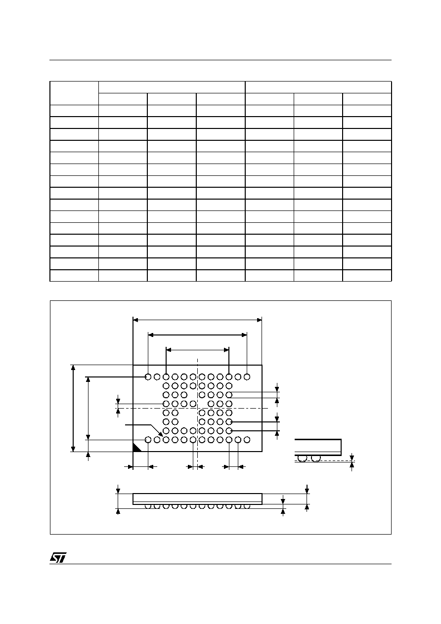
43/46
M36DR432A, M36DR432B
Table 37. Stacked LFBGA66 - 8 x 8 ball array, 0.8 mm pitch, Package Mechanical Data
Figure 25. Stacked LFBGA66 - 8 x 8 ball array, 0.8 mm pitch, Bottom View Package Outline
Note: Drawing is not to scale.
Symbol
millimeters
inches
Typ
Min
Max
Typ
Min
Max
A
1.400
0.0551
A1
0.250
0.0098
A2
1.100
0.0433
b
0.400
0.350
0.450
0.0157
0.0138
0.0177
D
12.000
≠
≠
0.4724
≠
≠
D1
5.600
≠
≠
0.2205
≠
≠
D2
8.800
≠
≠
0.3465
≠
≠
ddd
0.100
0.0039
E
8.000
≠
≠
0.3150
≠
≠
E1
5.600
≠
≠
0.2205
≠
≠
e
0.800
≠
≠
0.0315
≠
≠
FD
1.600
≠
≠
0.0630
≠
≠
FE
1.200
≠
≠
0.0472
≠
≠
SD
0.400
≠
≠
0.0157
≠
≠
SE
0.400
≠
≠
0.0157
≠
≠
A2
A1
A
BGA-Z12
ddd
D
E
e
b
SE
FD
FE
E1
e
D1
SD
D2
BALL "A1"
M36DR432A, M36DR432B
44/46
Figure 26. Stacked LFBGA66 Daisy Chain - Package Connections (Top view through package)
AI90251
D
C
#4
#3
8
7
6
1
E
F
A
B
H
G
5
4
3
2
#1
#2

45/46
M36DR432A, M36DR432B
Figure 27. Stacked LFBGA66 Daisy Chain - PCB Connections proposal (Top view through
package)
#1
AI90252
D
C
E
F
A
B
H
G
START
POINT
END
POINT
#4
#3
8
7
6
1
5
4
3
2
#2

M36DR432A, M36DR432B
46/46
Information furnished is believed to be accurate and reliable. However, STMicroelectronics assumes no responsibility for the consequences
of use of such information nor for any infringement of patents or other rights of third parties which may result from its use. No license is granted
by implication or otherwise under any patent or patent rights of STMicroelectronics. Specifications mentioned in this publication are subject
to change without notice. This publication supersedes and replaces all information previously supplied. STMicroelectronics products are not
authorized for use as critical components in life support devices or systems without express written approval of STMicroelectronics.
The ST logo is registered trademark of STMicroelectronics
All other names are the property of their respective owners.
©
2001 STMicroelectronics - All Rights Reserved
STMicroelectronics GROUP OF COMPANIES
Australia - Brazil - China - Finland - France - Germany - Hong Kong - India - Italy - Japan - Malaysia - Malta - Morocco -
Singapore - Spain - Sweden - Switzerland - United Kingdom - U.S.A.
www.st.com