
1/19
TARGET SPECIFICATION
July 2005
This is preliminary information on a new product forseen to be developed. Details are subject to change without notice.
M36LLR8760T1, M36LLR8760D1
M36LLR8760M1, M36LLR8760B1
256 + 128 Mbit (Multiple Bank, Multi-Level, Burst) Flash Memory
64 Mbit (Burst) PSRAM, 1.8V Supply, Multi-Chip Package
FEATURES SUMMARY
MULTI-CHIP PACKAGE
�
1 die of 256 Mbit (16Mb x16, Multiple
Bank, Multi-level, Burst) Flash Memory
�
1 die of 128 Mbit (8Mb x16, Multiple Bank,
Multi-Level, Burst) Flash Memory
�
1 die of 64 Mbit (4Mb x16) Pseudo SRAM
SUPPLY VOLTAGE
�
V
DDF1
= V
DDF2
= V
CCP
= V
DDQF
= 1.7 to
1.95V
�
V
PPF
= 9V for fast program (12V tolerant)
ELECTRONIC SIGNATURE
�
Manufacturer Code: 20h
�
Top Configuration (Top + Top)
M36LLR8760T1: 880Dh + 88C4h
�
Mixed Configuration (Bottom + Top)
M36LLR8760D1: 880Eh + 88C4h
�
Mixed Configuration (Top + Bottom)
M36LLR8760M1: 880Dh + 88C5h
�
Bottom Configuration (Bottom + Bottom)
M36LLR8760B1: 880Eh + 88C5h
PACKAGE
�
Compliant with Lead-Free Soldering
Processes
�
Lead-Free Versions
FLASH MEMORIES
SYNCHRONOUS / ASYNCHRONOUS READ
�
Synchronous Burst Read mode: 54MHz
�
Asynchronous Page Read mode
�
Random Access: 85ns
SYNCHRONOUS BURST READ SUSPEND
PROGRAMMING TIME
�
10�s typical Word program time using
Buffer Enhanced Factory Program
command
MEMORY ORGANIZATION
�
Multiple Bank Memory Array:
16 Mbit Banks for the 256 Mbit Memory
8 Mbit Banks for the 128 Mbit Memory
�
Parameter Blocks (at Top or Bottom)
Figure 1. Package
COMMON FLASH INTERFACE (CFI)
100,000 PROGRAM/ERASE CYCLES per
BLOCK
DUAL OPERATIONS
�
program/erase in one Bank while read in
others
�
No delay between read and write
operations
SECURITY
�
64 bit unique device number
�
2112 bit user programmable OTP Cells
BLOCK LOCKING
�
All blocks locked at power-up
�
Any combination of blocks can be locked
with zero latency
�
WP
F
for Block Lock-Down
�
Absolute Write Protection with V
PPF
= V
SS
PSRAM
ACCESS TIME: 70ns
ASYNCHRONOUS PAGE READ
�
Page Size: 16 words
�
Subsequent read within page: 20ns
LOW POWER FEATURES
�
Temperature Compensated Refresh
(TCR)
�
Partial Array Refresh (PAR)
�
Deep Power-Down (DPD) Mode
SYNCHRONOUS BURST READ/WRITE
LFBGA88 (ZAQ)
8 x 10mm
FBGA

M36LLR8760T1, M36LLR8760D1, M36LLR8760M1, M36LLR8760B1
2/19
TABLE OF CONTENTS
FEATURES SUMMARY . . . . . . . . . . . . . . . . . . . . . . . . . . . . . . . . . . . . . . . . . . . . . . . . . . . . . . . . . . . . . 1
FLASH MEMORIES . . . . . . . . . . . . . . . . . . . . . . . . . . . . . . . . . . . . . . . . . . . . . . . . . . . . . . . . . . . . . 1
Figure 1. Package. . . . . . . . . . . . . . . . . . . . . . . . . . . . . . . . . . . . . . . . . . . . . . . . . . . . . . . . . . . . . . . 1
PSRAM . . . . . . . . . . . . . . . . . . . . . . . . . . . . . . . . . . . . . . . . . . . . . . . . . . . . . . . . . . . . . . . . . . . . . . . 1
SUMMARY DESCRIPTION . . . . . . . . . . . . . . . . . . . . . . . . . . . . . . . . . . . . . . . . . . . . . . . . . . . . . . . . . . . 3
Figure 2. Logic Diagram . . . . . . . . . . . . . . . . . . . . . . . . . . . . . . . . . . . . . . . . . . . . . . . . . . . . . . . . . . 4
Table 1. Signal Names . . . . . . . . . . . . . . . . . . . . . . . . . . . . . . . . . . . . . . . . . . . . . . . . . . . . . . . . . . 4
Figure 3. LFBGA Connections (Top view through package) . . . . . . . . . . . . . . . . . . . . . . . . . . . . . . 5
SIGNAL DESCRIPTIONS . . . . . . . . . . . . . . . . . . . . . . . . . . . . . . . . . . . . . . . . . . . . . . . . . . . . . . . . . . . . 6
Address Inputs (A0-A23). . . . . . . . . . . . . . . . . . . . . . . . . . . . . . . . . . . . . . . . . . . . . . . . . . . . . . . . . . 6
Data Input/Output (DQ0-DQ15). . . . . . . . . . . . . . . . . . . . . . . . . . . . . . . . . . . . . . . . . . . . . . . . . . . . . 6
Latch Enable (L). . . . . . . . . . . . . . . . . . . . . . . . . . . . . . . . . . . . . . . . . . . . . . . . . . . . . . . . . . . . . . . . . 6
Clock (K).. . . . . . . . . . . . . . . . . . . . . . . . . . . . . . . . . . . . . . . . . . . . . . . . . . . . . . . . . . . . . . . . . . . . . . 6
Wait (WAIT). . . . . . . . . . . . . . . . . . . . . . . . . . . . . . . . . . . . . . . . . . . . . . . . . . . . . . . . . . . . . . . . . . . . 6
Flash Chip Enable Inputs (E
F1
, E
F2
).. . . . . . . . . . . . . . . . . . . . . . . . . . . . . . . . . . . . . . . . . . . . . . . . . 6
Flash Output Enable Inputs (G
F1
, G
F2
) . . . . . . . . . . . . . . . . . . . . . . . . . . . . . . . . . . . . . . . . . . . . . . . 6
Flash Write Enable (W
F
).. . . . . . . . . . . . . . . . . . . . . . . . . . . . . . . . . . . . . . . . . . . . . . . . . . . . . . . . . . 6
Flash Write Protect (WP
F
). . . . . . . . . . . . . . . . . . . . . . . . . . . . . . . . . . . . . . . . . . . . . . . . . . . . . . . . . 6
Flash Reset (RP
F
). . . . . . . . . . . . . . . . . . . . . . . . . . . . . . . . . . . . . . . . . . . . . . . . . . . . . . . . . . . . . . . 6
PSRAM Chip Enable input (E
P
). . . . . . . . . . . . . . . . . . . . . . . . . . . . . . . . . . . . . . . . . . . . . . . . . . . . . 7
PSRAM Write Enable (W
P
) . . . . . . . . . . . . . . . . . . . . . . . . . . . . . . . . . . . . . . . . . . . . . . . . . . . . . . . . 7
PSRAM Output Enable (G
P
) . . . . . . . . . . . . . . . . . . . . . . . . . . . . . . . . . . . . . . . . . . . . . . . . . . . . . . . 7
PSRAM Upper Byte Enable (UB
P
) . . . . . . . . . . . . . . . . . . . . . . . . . . . . . . . . . . . . . . . . . . . . . . . . . . 7
PSRAM Lower Byte Enable (LB
P
) . . . . . . . . . . . . . . . . . . . . . . . . . . . . . . . . . . . . . . . . . . . . . . . . . . . 7
PSRAM Configuration Register Enable (CR
P
) . . . . . . . . . . . . . . . . . . . . . . . . . . . . . . . . . . . . . . . . . 7
V
DDF1
/V
DDF2
Supply Voltages. . . . . . . . . . . . . . . . . . . . . . . . . . . . . . . . . . . . . . . . . . . . . . . . . . . . . . 7
V
CCP
Supply Voltage. . . . . . . . . . . . . . . . . . . . . . . . . . . . . . . . . . . . . . . . . . . . . . . . . . . . . . . . . . . . . 7
V
DDQF
Supply Voltage. . . . . . . . . . . . . . . . . . . . . . . . . . . . . . . . . . . . . . . . . . . . . . . . . . . . . . . . . . . . 7
V
PPF
Program Supply Voltage. . . . . . . . . . . . . . . . . . . . . . . . . . . . . . . . . . . . . . . . . . . . . . . . . . . . . . 7
V
SS
Ground.. . . . . . . . . . . . . . . . . . . . . . . . . . . . . . . . . . . . . . . . . . . . . . . . . . . . . . . . . . . . . . . . . . . . 7
FUNCTIONAL DESCRIPTION . . . . . . . . . . . . . . . . . . . . . . . . . . . . . . . . . . . . . . . . . . . . . . . . . . . . . . . . 8
Figure 4. Functional Block Diagram . . . . . . . . . . . . . . . . . . . . . . . . . . . . . . . . . . . . . . . . . . . . . . . . . 8
Table 2. Main Operating Modes . . . . . . . . . . . . . . . . . . . . . . . . . . . . . . . . . . . . . . . . . . . . . . . . . . . 9
MAXIMUM RATING. . . . . . . . . . . . . . . . . . . . . . . . . . . . . . . . . . . . . . . . . . . . . . . . . . . . . . . . . . . . . . . . 10
Table 3. Absolute Maximum Ratings . . . . . . . . . . . . . . . . . . . . . . . . . . . . . . . . . . . . . . . . . . . . . . . 10
DC AND AC PARAMETERS. . . . . . . . . . . . . . . . . . . . . . . . . . . . . . . . . . . . . . . . . . . . . . . . . . . . . . . . . 11
Table 4. Operating and AC Measurement Conditions . . . . . . . . . . . . . . . . . . . . . . . . . . . . . . . . . . 11
Figure 5. AC Measurement I/O Waveform . . . . . . . . . . . . . . . . . . . . . . . . . . . . . . . . . . . . . . . . . . . 11

3/19
M36LLR8760T1, M36LLR8760D1, M36LLR8760M1, M36LLR8760B1
Figure 6. AC Measurement Load Circuit. . . . . . . . . . . . . . . . . . . . . . . . . . . . . . . . . . . . . . . . . . . . . 11
Table 5. Device Capacitance. . . . . . . . . . . . . . . . . . . . . . . . . . . . . . . . . . . . . . . . . . . . . . . . . . . . . 11
Table 6. Flash 1 DC Characteristics - Currents . . . . . . . . . . . . . . . . . . . . . . . . . . . . . . . . . . . . . . . 12
Table 7. Flash 2 DC Characteristics - Currents . . . . . . . . . . . . . . . . . . . . . . . . . . . . . . . . . . . . . . . 13
Table 8. Flash 1 and Flash 2 DC Characteristics - Voltages . . . . . . . . . . . . . . . . . . . . . . . . . . . . . 14
Table 9. PSRAM DC Characteristics . . . . . . . . . . . . . . . . . . . . . . . . . . . . . . . . . . . . . . . . . . . . . . 14
PACKAGE MECHANICAL . . . . . . . . . . . . . . . . . . . . . . . . . . . . . . . . . . . . . . . . . . . . . . . . . . . . . . . . . . 15
Figure 7. LFBGA88 8x10mm, 8x10 ball array - 0.8mm pitch, Bottom View Package Outline . . . . 15
Table 10. Stacked LFBGA88 8x10mm - 8x10 active ball array, 0.8mm pitch, Package Data. . . . . 15
PART NUMBERING . . . . . . . . . . . . . . . . . . . . . . . . . . . . . . . . . . . . . . . . . . . . . . . . . . . . . . . . . . . . . . . 16
Table 11. Ordering Information Scheme . . . . . . . . . . . . . . . . . . . . . . . . . . . . . . . . . . . . . . . . . . . . . 16
REVISION HISTORY. . . . . . . . . . . . . . . . . . . . . . . . . . . . . . . . . . . . . . . . . . . . . . . . . . . . . . . . . . . . . . . 17
Table 12. Document Revision History . . . . . . . . . . . . . . . . . . . . . . . . . . . . . . . . . . . . . . . . . . . . . . . 17

M36LLR8760T1, M36LLR8760D1, M36LLR8760M1, M36LLR8760B1
4/19
SUMMARY DESCRIPTION
The M36LLR8760T1, M36LLR8760D1,
M36LLR8760M1 and M36LLR8760B1 combine
three memory devices in a Multi-Chip Package:
a 256-Mbit, Multiple Bank Flash memory, the
M30L0R8000(T/B)0 (Flash 1)
a 128-Mbit, Multiple Bank Flash memory, the
M58LR128GT/B (Flash 2)
a 64-Mbit PseudoSRAM, the M69KB096AA.
For detailed information on how to use the memo-
ry components, refer to the M30L0R8000(T/B)0,
M58LR128GT/B and M69KB096AA datasheets
which are available from your local STMicroelec-
tronics distributor and should be read in conjunc-
tion with the M36LLR8760x1 datasheet.
What differs between the M36LLR8760T1,
M36LLR8760D1 and M36LLR8760B1 is the con-
figuration of the two Flash memories:
in the M36LLR8760T1, Flash 1 and Flash 2
both have a Top Configuration (Parameter
Blocks located at the top of the address
space).
in the M36LLR8760D1, Flash 1 has a Bottom
Configuration (Parameter Blocks at the
bottom of the address space) and Flash 2 has
a Top Configuration.
In the M36LLR8760M1, Flash 1 has a Top
Configuration and Flash 2 has a Bottom
Configuration.
In the M36LLR8760B1, both Flash 1 and
Flash 2 have a Bottom Configuration.
Recommended operating conditions do not allow
more than one memory to be active at the same
time.
The memories are offered in a Stacked LFBGA88
(8 x 10mm, 8x10 ball array, 0.8mm pitch) pack-
age.
In addition to the standard version, the package is
also available in Lead-free version, in compliance
with JEDEC Std J-STD-020B, the ST ECOPACK
7191395 Specification, and the RoHS (Restriction
of Hazardous Substances) directive. All packages
are compliant with Lead-free soldering processes.
The memory is supplied with all the bits erased
(set to `1').
5/19
M36LLR8760T1, M36LLR8760D1, M36LLR8760M1, M36LLR8760B1
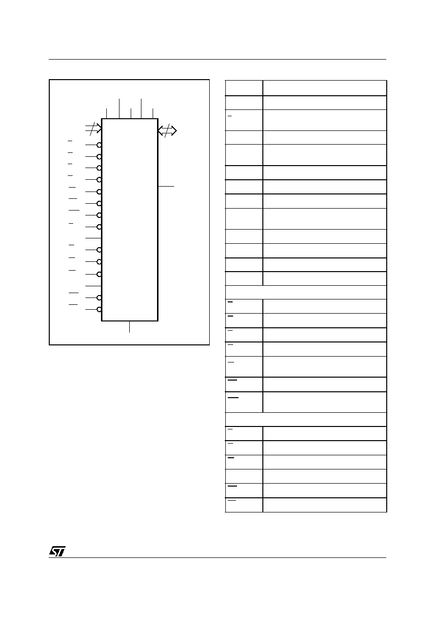
Figure 2. Logic Diagram
Table 1. Signal Names
Note: 1. A22 is an Address Input for the two Flash memories only.
A23 is for the 256Mb Flash memory component only.
AI10908b
24
A0-A23
DQ0-DQ15
M36LLR8760T1
M36LLR8760D1
M36LLR8760M1
M36LLR8760B1
G
F1
16
W
F
RP
F
WP
F
E
P
G
P
W
P
UB
P
LB
P
VSS
V
PPF
V
CCP
WAIT
L
K
V
DDQF
E
F1
CR
P
V
DDF2
V
DDF1
G
F2
E
F2
A0-A23
(1)
Address Inputs
DQ0-DQ15 Common Data Input/Output
L
Common Flash and PSRAM Latch
Enable Input
K
Common Flash and PSRAM Burst Clock
WAIT
Wait Data in Burst Mode for both Flash
memories and PSRAM
V
DDF1
Flash 1 Power Supply
V
DDF2
Flash 2 Power Supply
V
DDQF
Common Flash Supply for I/O Buffers
V
PPF
Common Flash Optional Supply Voltage
for Fast Program & Erase
V
SS
Common, Ground
V
CCP
PSRAM Power Supply
NC
Not Connected Internally
DU
Do Not Use as Internally Connected
Flash Memory Signals
E
F1
Flash 1 Chip Enable Input
G
F1
Flash 1 Output Enable Input
E
F2
Flash 2 Chip Enable Input
G
F2
Flash 2 Output Enable Input
W
F
Common Flash Memory Write Enable
Input
RP
F
Common Flash Memory Reset input
WP
F
Common Flash Memory Write Protect
Input
PSRAM Signals
E
P
Chip Enable Input
G
P
Output Enable Input
W
P
Write Enable Input
CR
P
Configuration Register Enable Input
UB
P
Upper Byte Enable Input
LB
P
Lower Byte Enable Input