1/17
December 2004
M36W0R6050T0
M36W0R6050B0
64 Mbit (4Mb x16, Multiple Bank, Burst) Flash Memory
and 32 Mbit (2Mb x16) PSRAM, Multi-Chip Package
FEATURES SUMMARY
MULTI-CHIP PACKAGE
1 die of 64 Mbit (4Mb x 16) Flash Memory
1 die of 32 Mbit (2Mb x 16) Pseudo SRAM
SUPPLY VOLTAGE
V
DDF
= V
CCP
= V
DDQ
= 1.7V to 1.95V
LOW POWER CONSUMPTION
ELECTRONIC SIGNATURE
Manufacturer Code: 20h
Device Code (Top Flash Configuration),
M36W0R6050T0: 8810h
Device Code (Bottom Flash
Configuration), M36W0R6050B0: 8811h
PACKAGE
Compliant with Lead-Free Soldering
Processes
Lead-Free Versions
FLASH MEMORY
PROGRAMMING TIME
8µs by Word typical for Fast Factory
Program
Double/Quadruple Word Program option
Enhanced Factory Program options
MEMORY BLOCKS
Multiple Bank Memory Array: 4 Mbit
Banks
Parameter Blocks (Top location)
SYNCHRONOUS / ASYNCHRONOUS READ
Synchronous Burst Read mode: 66MHz
Asynchronous/ Synchronous Page Read
mode
Random Access: 70ns
DUAL OPERATIONS
Program Erase in one Bank while Read in
others
No delay between Read and Write
operations
BLOCK LOCKING
All blocks locked at Power-up
Any combination of blocks can be locked
WP
F
for Block Lock-Down
Figure 1. Package
SECURITY
128-bit user programmable OTP cells
64-bit unique device number
COMMON FLASH INTERFACE (CFI)
100,000 PROGRAM/ERASE CYCLES per
BLOCK
PSRAM
ACCESS TIMES: 85ns
LOW STANDBY CURRENT: 100µA
DEEP POWER DOWN CURRENT: 10µA
BYTE CONTROL: UB
P
/LB
P
PROGRAMMABLE PARTIAL ARRAY
TRI-STATE COMMON I/O
8 WORD PAGE ACCESS CAPABILITY: 25ns
PARTIAL POWER-DOWN MODES
Deep Power-Down
4 Mbit Partial Power-Down
8 Mbit Partial Power-Down
16 Mbit Partial Power-Down
FBGA
Stacked TFBGA88 (ZAQ)
8 x 10mm

M36W0R6050T0, M36W0R6050B0
2/17
TABLE OF CONTENTS
FEATURES SUMMARY . . . . . . . . . . . . . . . . . . . . . . . . . . . . . . . . . . . . . . . . . . . . . . . . . . . . . . . . . . . . . 1
FLASH MEMORY . . . . . . . . . . . . . . . . . . . . . . . . . . . . . . . . . . . . . . . . . . . . . . . . . . . . . . . . . . . . . . . 1
Figure 1. Package. . . . . . . . . . . . . . . . . . . . . . . . . . . . . . . . . . . . . . . . . . . . . . . . . . . . . . . . . . . . . . . 1
PSRAM . . . . . . . . . . . . . . . . . . . . . . . . . . . . . . . . . . . . . . . . . . . . . . . . . . . . . . . . . . . . . . . . . . . . . . . 1
SUMMARY DESCRIPTION . . . . . . . . . . . . . . . . . . . . . . . . . . . . . . . . . . . . . . . . . . . . . . . . . . . . . . . . . . . 4
Figure 2. Logic Diagram . . . . . . . . . . . . . . . . . . . . . . . . . . . . . . . . . . . . . . . . . . . . . . . . . . . . . . . . . . 4
Table 1. Signal Names . . . . . . . . . . . . . . . . . . . . . . . . . . . . . . . . . . . . . . . . . . . . . . . . . . . . . . . . . . 4
Figure 3. TFBGA Connections (Top view through package) . . . . . . . . . . . . . . . . . . . . . . . . . . . . . . 5
SIGNAL DESCRIPTIONS . . . . . . . . . . . . . . . . . . . . . . . . . . . . . . . . . . . . . . . . . . . . . . . . . . . . . . . . . . . . 6
Address Inputs (A0-A20). . . . . . . . . . . . . . . . . . . . . . . . . . . . . . . . . . . . . . . . . . . . . . . . . . . . . . . . . . 6
Address Input (A21). . . . . . . . . . . . . . . . . . . . . . . . . . . . . . . . . . . . . . . . . . . . . . . . . . . . . . . . . . . . . . 6
Data Input/Output (DQ0-DQ15). . . . . . . . . . . . . . . . . . . . . . . . . . . . . . . . . . . . . . . . . . . . . . . . . . . . . 6
Flash Chip Enable (E
F
).. . . . . . . . . . . . . . . . . . . . . . . . . . . . . . . . . . . . . . . . . . . . . . . . . . . . . . . . . . . 6
Flash Output Enable (G
F
). . . . . . . . . . . . . . . . . . . . . . . . . . . . . . . . . . . . . . . . . . . . . . . . . . . . . . . . . . 6
Flash Write Enable (W
F
).. . . . . . . . . . . . . . . . . . . . . . . . . . . . . . . . . . . . . . . . . . . . . . . . . . . . . . . . . . 6
Flash Write Protect (WP
F
). . . . . . . . . . . . . . . . . . . . . . . . . . . . . . . . . . . . . . . . . . . . . . . . . . . . . . . . . 6
Flash Reset (RP
F
). . . . . . . . . . . . . . . . . . . . . . . . . . . . . . . . . . . . . . . . . . . . . . . . . . . . . . . . . . . . . . . 6
Flash Latch Enable (L
F
). . . . . . . . . . . . . . . . . . . . . . . . . . . . . . . . . . . . . . . . . . . . . . . . . . . . . . . . . . . 6
Flash Clock (K
F
). . . . . . . . . . . . . . . . . . . . . . . . . . . . . . . . . . . . . . . . . . . . . . . . . . . . . . . . . . . . . . . . . 6
Flash Wait (WAIT
F
).. . . . . . . . . . . . . . . . . . . . . . . . . . . . . . . . . . . . . . . . . . . . . . . . . . . . . . . . . . . . . . 6
PSRAM Chip Enable (E1
P
).. . . . . . . . . . . . . . . . . . . . . . . . . . . . . . . . . . . . . . . . . . . . . . . . . . . . . . . . 6
PSRAM Chip Enable (E2
P
).. . . . . . . . . . . . . . . . . . . . . . . . . . . . . . . . . . . . . . . . . . . . . . . . . . . . . . . . 6
PSRAM Output Enable (G
P
).. . . . . . . . . . . . . . . . . . . . . . . . . . . . . . . . . . . . . . . . . . . . . . . . . . . . . . . 7
PSRAM Write Enable (W
P
).. . . . . . . . . . . . . . . . . . . . . . . . . . . . . . . . . . . . . . . . . . . . . . . . . . . . . . . . 7
PSRAM Upper Byte Enable (UB
P
). . . . . . . . . . . . . . . . . . . . . . . . . . . . . . . . . . . . . . . . . . . . . . . . . . . 7
PSRAM Lower Byte Enable (LB
P
). . . . . . . . . . . . . . . . . . . . . . . . . . . . . . . . . . . . . . . . . . . . . . . . . . . 7
V
DDF
Supply Voltage . . . . . . . . . . . . . . . . . . . . . . . . . . . . . . . . . . . . . . . . . . . . . . . . . . . . . . . . . . . . . 7
V
CCP
Supply Voltage. . . . . . . . . . . . . . . . . . . . . . . . . . . . . . . . . . . . . . . . . . . . . . . . . . . . . . . . . . . . . 7
V
DDQ
Supply Voltage. . . . . . . . . . . . . . . . . . . . . . . . . . . . . . . . . . . . . . . . . . . . . . . . . . . . . . . . . . . . . 7
V
PPF
Program Supply Voltage. . . . . . . . . . . . . . . . . . . . . . . . . . . . . . . . . . . . . . . . . . . . . . . . . . . . . . 7
V
SS
Ground.. . . . . . . . . . . . . . . . . . . . . . . . . . . . . . . . . . . . . . . . . . . . . . . . . . . . . . . . . . . . . . . . . . . . 7
FUNCTIONAL DESCRIPTION . . . . . . . . . . . . . . . . . . . . . . . . . . . . . . . . . . . . . . . . . . . . . . . . . . . . . . . . 8
Figure 4. Functional Block Diagram . . . . . . . . . . . . . . . . . . . . . . . . . . . . . . . . . . . . . . . . . . . . . . . . . 8
Table 2. Main Operating Modes . . . . . . . . . . . . . . . . . . . . . . . . . . . . . . . . . . . . . . . . . . . . . . . . . . . 9
FLASH MEMORY DEVICE . . . . . . . . . . . . . . . . . . . . . . . . . . . . . . . . . . . . . . . . . . . . . . . . . . . . . . . . . . 10
PSRAM DEVICE . . . . . . . . . . . . . . . . . . . . . . . . . . . . . . . . . . . . . . . . . . . . . . . . . . . . . . . . . . . . . . . . . . 10
MAXIMUM RATING. . . . . . . . . . . . . . . . . . . . . . . . . . . . . . . . . . . . . . . . . . . . . . . . . . . . . . . . . . . . . . . . 10
Table 3. Absolute Maximum Ratings . . . . . . . . . . . . . . . . . . . . . . . . . . . . . . . . . . . . . . . . . . . . . . . 10

3/17
M36W0R6050T0, M36W0R6050B0
DC AND AC PARAMETERS. . . . . . . . . . . . . . . . . . . . . . . . . . . . . . . . . . . . . . . . . . . . . . . . . . . . . . . . . 11
Table 4. Operating and AC Measurement Conditions . . . . . . . . . . . . . . . . . . . . . . . . . . . . . . . . . . 11
Figure 5. AC Measurement I/O Waveform . . . . . . . . . . . . . . . . . . . . . . . . . . . . . . . . . . . . . . . . . . . 11
Figure 6. AC Measurement Load Circuit. . . . . . . . . . . . . . . . . . . . . . . . . . . . . . . . . . . . . . . . . . . . . 11
Table 5. Device Capacitance. . . . . . . . . . . . . . . . . . . . . . . . . . . . . . . . . . . . . . . . . . . . . . . . . . . . . 11
Table 6. Flash Memory DC Characteristics - Currents . . . . . . . . . . . . . . . . . . . . . . . . . . . . . . . . . 12
Table 7. Flash Memory DC Characteristics - Voltages . . . . . . . . . . . . . . . . . . . . . . . . . . . . . . . . . 13
Table 8. PSRAM DC Characteristics . . . . . . . . . . . . . . . . . . . . . . . . . . . . . . . . . . . . . . . . . . . . . . . 13
PACKAGE MECHANICAL . . . . . . . . . . . . . . . . . . . . . . . . . . . . . . . . . . . . . . . . . . . . . . . . . . . . . . . . . . 14
Figure 7. Stacked TFBGA88 8x10mm - 8x10 active ball array, 0.8mm pitch, Package Outline . . 14
Table 9. Stacked TFBGA88 8x10mm - 8x10 ball array, 0.8mm pitch, Package Mechanical Data 14
PART NUMBERING . . . . . . . . . . . . . . . . . . . . . . . . . . . . . . . . . . . . . . . . . . . . . . . . . . . . . . . . . . . . . . . 15
Table 10. Ordering Information Scheme . . . . . . . . . . . . . . . . . . . . . . . . . . . . . . . . . . . . . . . . . . . . . 15
REVISION HISTORY . . . . . . . . . . . . . . . . . . . . . . . . . . . . . . . . . . . . . . . . . . . . . . . . . . . . . . . . . . . . . . . 16
Table 11. Document Revision History . . . . . . . . . . . . . . . . . . . . . . . . . . . . . . . . . . . . . . . . . . . . . . . 16
M36W0R6050T0, M36W0R6050B0
4/17
SUMMARY DESCRIPTION
The M36W0R6050T0 and M36W0R6050B0 com-
bine two memory devices in a Multi-Chip Package:
a 64-Mbit, Multiple Bank Flash memory, the
M58WR064FT/B, and a 32-Mbit Pseudo SRAM,
the M69AR048B. Recommended operating condi-
tions do not allow more than one memory to be ac-
tive at the same time.
The memory is offered in a Stacked TFBGA88
(8 x 10mm, 8x10 ball array, 0.8mm pitch) pack-
age.
In addition to the standard version, the packages
are also available in Lead-free version, in compli-
ance with JEDEC Std J-STD-020B, the ST ECO-
PACK 7191395 Specification, and the RoHS
(Restriction of Hazardous Substances) directive.
All packages are compliant with Lead-free solder-
ing processes.
The memory is supplied with all the bits erased
(set to `1').
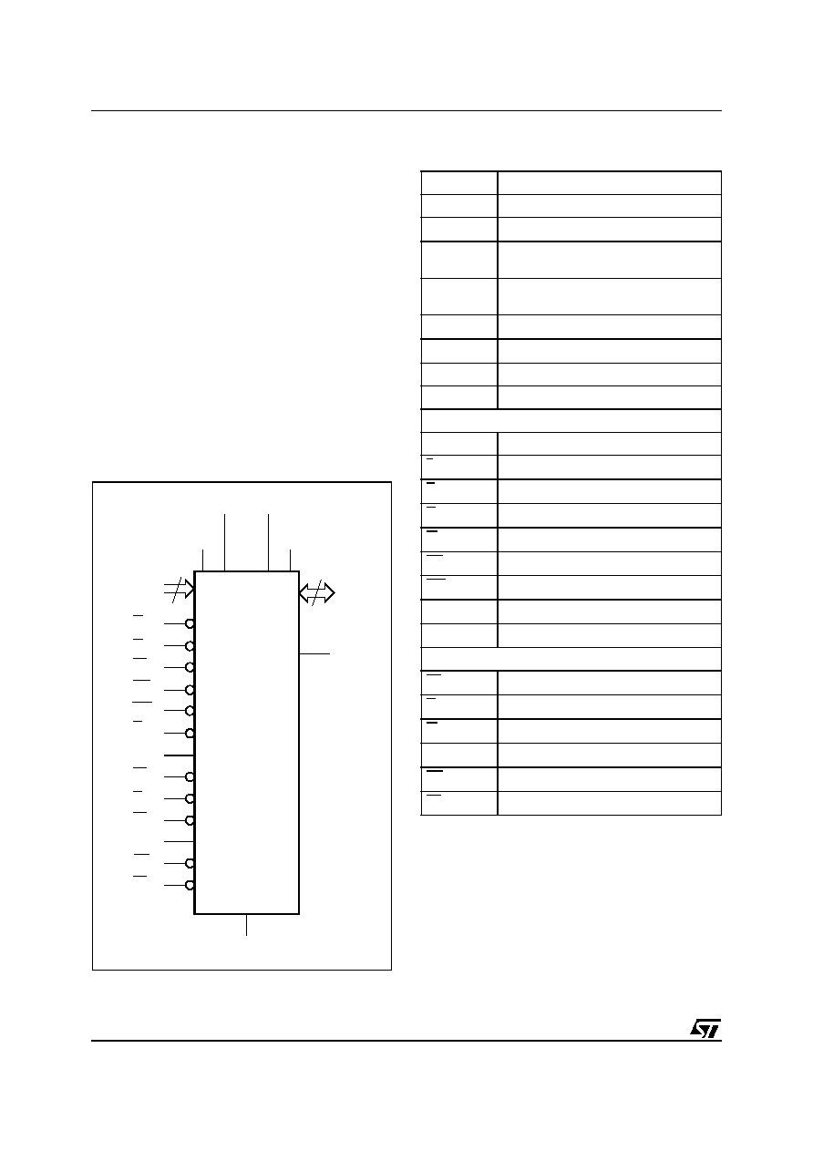
Figure 2. Logic Diagram
Table 1. Signal Names
AI09378
22
A0-A21
DQ0-DQ15
M36W0R6050T0
M36W0R6050B0
G
F
16
W
F
RP
F
WP
F
E1
P
G
P
W
P
UB
P
LB
P
VSS
V
DDF
V
PPF
V
CCP
WAIT
F
L
F
K
F
V
DDQ
E
F
E2
P
A0-A20
Common Address Inputs
DQ0-DQ15
Common Data Input/Output
V
DDF
Flash Memory Power Supply
V
DDQ
Common Flash and PSRAM Power
Supply for I/O Buffers
V
PPF
Common Flash Optional Supply Voltage
for Fast Program & Erase
V
SS
Ground
V
CCP
PSRAM Power Supply
NC
Not Connected Internally
DU
Do Not Use as Internally Connected
Flash Memory
A21
Address Input for the Flash memory only
L
F
Latch Enable input
E
F
Chip Enable input
G
F
Output Enable input
W
F
Write Enable input
RP
F
Reset input
WP
F
Write Protect input
K
F
Burst Clock
WAIT
F
Wait Data in Burst Mode
PSRAM
E1
P
Chip Enable input
G
P
Output Enable input
W
P
Write Enable input
E2
P
Power-down input
UB
P
Upper Byte Enable input
LB
P
Lower Byte Enable input