1/35
NOT FOR NEW DESIGN
May 1999
This is information on a product still in production but not recommended for new designs.
M36W108T
M36W108B
8 Mbit (1Mb x8, Boot Block) Flash Memory and
1 Mbit (128Kb x8) SRAM Low Voltage Multi-Memory Product
s
M36W108T and M36W108B are replaced
respectively by the M36W108AT and
M36W108AB
s
SUPPLY VOLTAGE
≠ V
CCF
= V
CCS
= 2.7V to 3.6V: for Program,
Erase and Read
s
ACCESS TIME: 100ns
s
LOW POWER CONSUMPTION
≠ Read: 40mA max. (SRAM chip)
≠ Stand-by: 30µA max. (SRAM chip)
≠ Read: 10mA max. (Flash chip)
≠ Stand-by: 100µA max. (Flash chip)
FLASH MEMORY
s
8 Mbit (1Mb x 8) BOOT BLOCK ERASE
s
PROGRAMMING TIME: 10µs typical
s
PROGRAM/ERASE CONTROLLER (P/E.C.)
≠ Program Byte-by-Byte
≠ Status Register bits and Ready/Busy Output
s
MEMORY BLOCKS
≠ Boot Block (Top or Bottom location)
≠ Parameter and Main Blocks
s
BLOCK, MULTI-BLOCK and CHIP ERASE
s
ERASE SUSPEND and RESUME MODES
≠ Read and Program another Block during
Erase Suspend
s
100,000 PROGRAM/ERASE CYCLES per
BLOCK
s
ELECTRONIC SIGNATURE
≠ Manufacturer Code: 20h
≠ Device Code, M36W108T: D2h
≠ Device Code, M36W108B: DCh
SRAM
s
1 Mbit (128Kb x 8)
s
POWER DOWN FEATURES USING TWO
CHIP ENABLE INPUTS
s
LOW V
CC
DATA RETENTION: 2V
BGA
LGA
LBGA48 (ZM)
6 x 8 solder balls
LGA48 (ZN)
6 x 8 solder lands
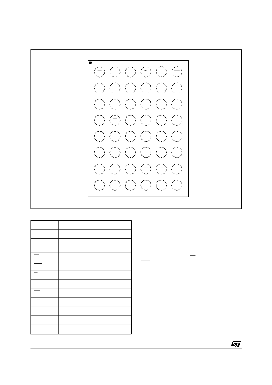
Figure 1. Logic Diagram
AI02509
20
A0-A19
W
DQ0-DQ7
VCCF
M36W108T
M36W108B
EF
VSS
8
G
RP
RB
VCCS
E1S
E2S
M36W108T, M36W108B
2/35
DESCRIPTION
The M36W108 is multi-chip device containing an
8 Mbit boot block Flash memory and a 1 Mbit of
SRAM. The device is offered in the new Chip
Scale Package solutions: LBGA48 1.0 mm ball
pitch and LGA48 1.0 mm land pitch.
The two components, of the package's overall 9
Mbit of memory, are distinguishable by use of the
three chip enable lines: EF for the Flash memory,
E1S and E2S for the SRAM.
The Flash memory component is identical with the
M29W008 device. It is a non-volatile memory that
may be erased electrically at the block or chip level
and programmed in-system on a Byte-by-Byte ba-
sis using only a single 2.7V to 3.6V V
CCF
supply.
For Program and Erase operations the necessary
high voltages are generated internally. The device
can also be programmed in standard program-
mers. The array matrix organization allows each
block to be erased and reprogrammed without af-
fecting other blocks.
Instructions for Read/Reset, Auto Select for read-
ing the Electronic Signature, Programming, Block
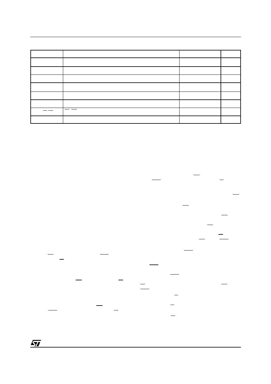
Figure 2. LBGA and LGA Connections (Top View)
C
B
A
6
5
4
3
2
1
E
D
F
G
A11
A14
A1
NC
EF
VSS
A2
A3
DQ3
NC
NC
A4
A7
VCCF
NC
A0
VSS
A8
A18
VCCS
DQ1
DQ2
DQ4
A5
NC
W
DQ7
DQ5
A19
NC
A6
DQ0
A10
E1S
AI02508
G
H
E2S
RB
A13
DQ6
NC
A9
A15
A12
NC
A16
NC
RP
A17
Table 1. Signal Names
A0-A16
Address Inputs
A17-A19
Address Inputs for Flash Chip
DQ0-DQ7
Data Input/Outputs, Command Inputs
for Flash Chip
EF
Chip Enable for Flash Chip
E1S, E2S
Chip Enable for SRAM Chip
G
Output Enable
W
Write Enable
RP
Reset for Flash Chip
RB
Ready/Busy Output for Flash Chip
V
CCF
Supply Voltage for Flash Chip
V
CCS
Supply Voltage for SRAM Chip
V
SS
Ground
3/35
M36W108T, M36W108B
and Chip Erase, Erase Suspend and Resume are
written to the device in cycles of commands to a
Command Interface using standard microproces-
sor write timings.
The SRAM component is a low power SRAM that
features fully static operation requiring no external
clocks or timing strobes, with equal address ac-
cess and cycle times. It requires a single 2.7V to
3.6V V
CCS
supply, and all inputs and outputs are
TTL compatible.
SIGNAL DESCRIPTIONS
See Figure 1 and Table 1.
Address Inputs (A0-A16). Addresses A0 to A16
are common inputs for the Flash chip and the
SRAM chip. The address inputs for the Flash
memory or the SRAM array are latched during a
write operation on the falling edge of Flash Chip
Enable (EF), SRAM Chip Enable (E1S or E2S) or
Write Enable (W).
Address Inputs (A17-A19). Address A17 to A19
are address inputs for the Flash chip. They are
latched during a write operation on the falling edge
of Flash Chip Enable (EF) or Write Enable (W).
Data Input/Outputs (DQ0-DQ7). The input is
data to be programmed in the Flash or SRAM
memory array or a command to be written to the
C.I. of the Flash chip. Both are latched on the ris-
ing edge of Flash Chip Enable (EF), SRAM Chip
Enable (E1S or E2S) or Write Enable (W). The
output is data from the Flash memory or SRAM ar-
ray, the Electronic Signature Manufacturer or De-
vice codes or the Status register Data Polling bit
DQ7, the Toggle Bits DQ6 and DQ2, the Error bit
DQ5 or the Erase Timer bit DQ3. Outputs are valid
when Flash Chip Enable (EF) or SRAM Chip En-
able (E1S or E2S) and Output Enable (G) are ac-
tive. The output is high impedance when the both
the Flash chip and the SRAM chip are deselected
or the outputs are disabled and when Reset (RP)
is at a V
IL
.
Flash Chip Enable (EF). The Chip Enable input
for Flash activates the memory control logic, input
buffers, decoders and sense amplifiers. EF at V
IH
deselects the memory and reduces the power con-
sumption to the standby level. EF can also be
used to control writing to the command register
and to the Flash memory array, while W remains
at V
IL
. It is not allowed to set EF at V
IL
, E1S at V
IL
and E2S at V
IH
at the same time.
SRAM Chip Enable (E1S, E2S). The Chip En-
able inputs for SRAM activate the memory control
logic, input buffers, decoders and sense amplifi-
ers. E1S at V
IH
or E2S at V
IL
deselects the mem-
ory and reduces the power consumption to the
standby level. E1S and E2S can also be used to
control writing to the SRAM memory array, while
W remains at V
IL
. It is not allowed to set EF at V
IL
,
E1S at V
IL
and E2S at V
IH
at the same time.
Output Enable (G). The Output Enable gates the
outputs through the data buffers during a read op-
eration. When G is High the outputs are High im-
pedance.
Write Enable (W). The Write Enable input con-
trols writing to the Command Register of the Flash
chip and Address/Data latches.
Table 2. Absolute Maximum Ratings
(1)
Note: 1. Except for the rating "Operating Temperature Range", stresses above those listed in the Table "Absolute Maximum Ratings" may
cause permanent damage to the device. These are stress ratings only and operation of the device at these or any other conditions
above those indicated in the Operating sections of this specification is not implied. Exposure to Absolute Maximum Rating condi-
tions for extended periods may affect device reliability. Refer also to the STMicroelectronics SURE Program and other relevant qual-
ity documents.
2. Minimum Voltage may undershoot to ≠2V during transition and for less than 20ns.
3. Depends on range.
Symbol
Parameter
Value
Unit
T
A
Ambient Operating Temperature
(3)
≠40 to 85
∞C
T
BIAS
Temperature Under Bias
≠50 to 125
∞C
T
STG
Storage Temperature
≠65 to 150
∞C
V
IO
(2)
Input or Output Voltage
≠0.5 to V
CC
+0.5
V
V
CCF
Flash Chip Supply Voltage
≠0.6 to 5
V
V
CCS
SRAM Chip Supply Voltage
≠0.3 to 4.6
V
V
(EF, RP)
EF, RP Voltage
0.6 to 13.5
V
PD
Power Dissipation
0.7
W

M36W108T, M36W108B
4/35
Reset Input (RP). The Reset input provides
hardware reset of the Flash chip. Reset of the
Flash memory is achieved by pulling RP to V
IL
for
at least t
PLPX
. When the reset pulse is given, if the
Flash memory is in Read or Standby modes, it will
be available for new operations in t
PHEL
after the
rising edge of RP.
If the Flash memory is in Erase or Program mode
the reset will take t
PLYH
during which the Ready/
Busy (RB) signal will be held at V
IL
. The end of the
Flash memory reset will be indicated by the rising
edge of RB. A hardware reset during an Erase or
Program operation will corrupt the data being pro-
grammed or the block(s) being erased. See Table
17 and Figure 9.
Ready/Busy Output (RB). Ready/Busy is an
open-drain output of the Flash chip. It gives the in-
ternal state of the Program/Erase Controller (P/
E.C.) of the Flash device. When RB is Low, the
Flash device is busy with a Program or Erase op-
eration and it will not accept any additional pro-
gram or erase instructions except the Erase
Suspend instruction. When RB is High, the Flash
device is ready for any Read, Program or Erase
operation. The RB will also be High when the
Flash memory is put in Erase Suspend or Standby
modes.
V
CCF
Supply Voltage. Flash memory power sup-
ply for all operations (Read, Program and Erase).
V
CCS
Supply Voltage. SRAM power supply for
all operations (Read, Program).
V
SS
Ground. V
SS
is the reference for all voltage
measurements.
POWER SUPPLY
Power Up. The Flash memory Command Inter-
face is reset on power up to Read Array. Either
Flash Chip Enable (EF) or Write Enable (W) inputs
must be tied to V
IH
during Power Up to allow max-
imum security and the possibility to write a com-
mand on the first rising edge of EF and W. Any
write cycle initiation is blocked when V
CCF
is below
V
LKO
.
Supply Rails. Normal precautions must be taken
for supply voltage decoupling; each device in a
system should have the V
CCF
, V
CCS
rails decou-
pled with a 0.1µF capacitor close to the V
CCF
,
V
CCS
and V
SS
pins. The PCB trace widths should
be sufficient to carry the V
CCF
and V
CCS
program
currents and the V
CCF
erase current required.
Table 3. Main Operation Modes
(1)
Note: 1. X = V
IL
or V
IH
.
Operation Mode
EF
E1S
E2S
G
W
RP
DQ0-DQ7
Flash Chip Read
V
IL
V
IH
X
V
IL
V
IH
V
IH
Data Output
V
IL
X
V
IL
V
IL
V
IH
V
IH
Data Output
SRAM Chip Read
V
IH
V
IL
V
IH
V
IL
V
IH
X
Data Output
Flash Chip Write
V
IL
V
IH
X
V
IH
V
IL
V
IH
Data Input
V
IL
X
V
IL
V
IH
V
IL
V
IH
Data Input
SRAM Chip Write
V
IH
V
IL
V
IH
X
V
IL
X
Data Input
Flash Chip Output Disable
X
V
IH
X
V
IH
V
IH
X
Hi-Z
X
X
V
IL
V
IH
V
IH
X
Hi-Z
SRAM Chip Output Disable
V
IH
V
IL
V
IH
V
IH
V
IH
X
Hi-Z
Flash Chip Stand-by
V
IH
X
X
X
X
V
IH
Hi-Z
Flash Chip Reset
X
V
IH
X
X
X
V
IL
Hi-Z
X
X
V
IL
X
X
V
IL
Hi-Z
SRAM Chip Stand-by
X
V
IH
X
X
X
V
IL
Hi-Z
X
X
V
IL
X
X
V
IL
Hi-Z

5/35
M36W108T, M36W108B
Figure 3. Internal Functional Arrangement
AI02444
VCCS
8 Mbit
Flash Memory
(1Mb x 8)
RP
RB
EF
W
G
1 Mbit SRAM
(128 Kb x 8)
A0-A16
E1S
E2S
VSS
VCCF
VSS
A0-A19
DQ0-DQ7