Äîêóìåíòàöèÿ è îïèñàíèÿ www.docs.chipfind.ru
1/64
May 2003
M36W832TE
M36W832BE
32 Mbit (2Mb x16, Boot Block) Flash Memory
and 8 Mbit (512Kb x16) SRAM, Multiple Memory Product
FEATURES SUMMARY
s
SUPPLY VOLTAGE
V
DDF
= 2.7V to 3.3V
V
DDS
= V
DDQF
= 2.7V to 3.3V
V
PPF
= 12V for Fast Program (optional)
s
ACCESS TIMES: 70ns and 85ns
s
LOW POWER CONSUMPTION
s
ELECTRONIC SIGNATURE
Manufacturer Code: 20h
Top Device Code, M36W832TE: 88BAh
Bottom Device Code, M36W832BE: 88BBh
FLASH MEMORY
s
32 Mbit (2Mb x16) BOOT BLOCK
8 x 4 KWord Parameter Blocks (Top or
Bottom Location)
s
PROGRAMMING TIME
10µs typical
Double Word Programming Option
Quadruple Word Programming Option
s
BLOCK LOCKING
All blocks locked at Power up
Any combination of blocks can be locked
WPF for Block Lock-Down
s
AUTOMATIC STANDBY MODE
s
PROGRAM and ERASE SUSPEND
s
100,000 PROGRAM/ERASE CYCLES per
BLOCK
s
COMMON FLASH INTERFACE
s
SECURITY
128 bit user programmable OTP cells
64 bit unique device identifier
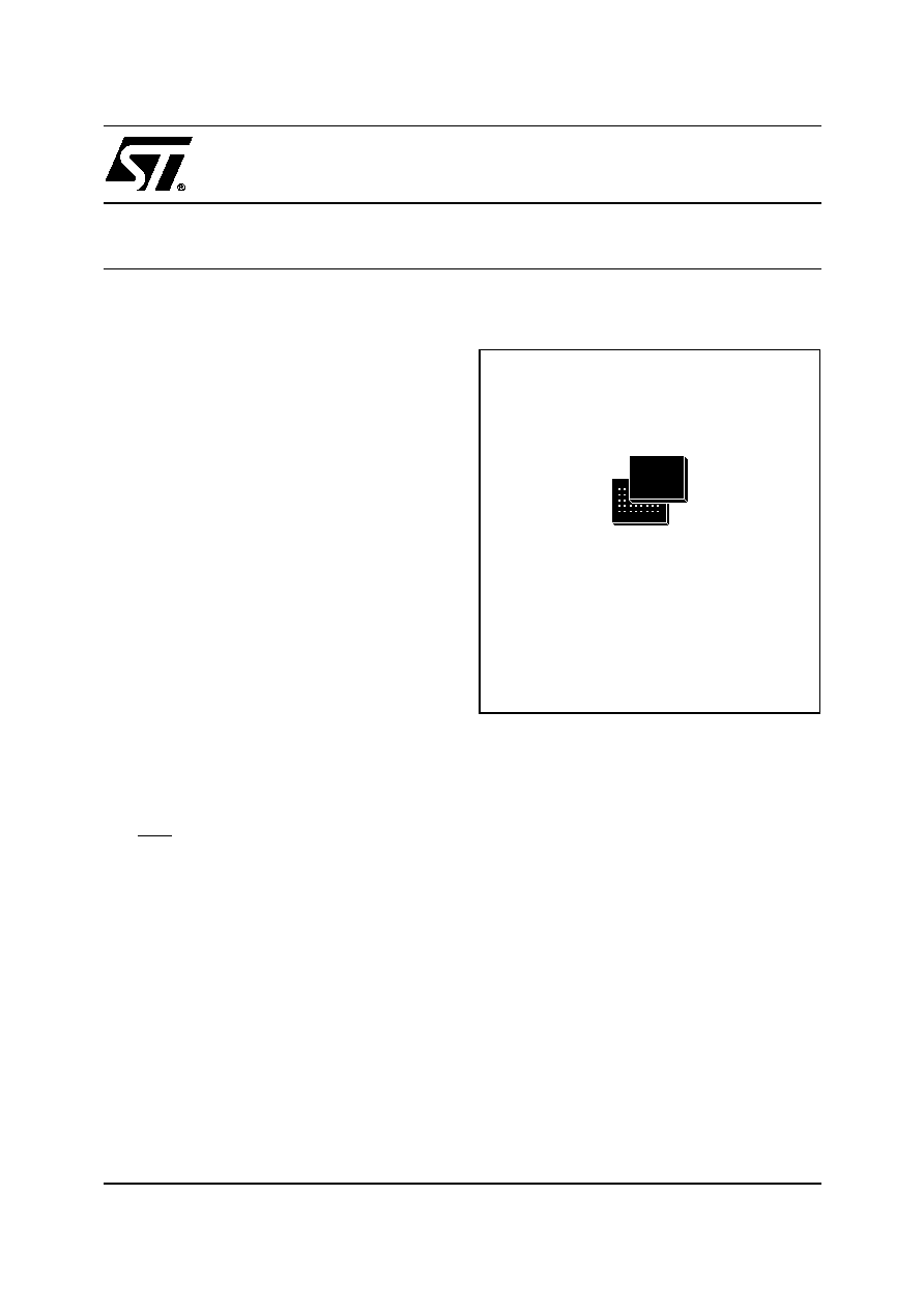
Figure 1. Packages
SRAM
s
8 Mbit (512Kb x 16)
s
ACCESS TIME: 70ns
s
LOW V
DDS
DATA RETENTION: 1.5V
s
POWER DOWN FEATURES USING TWO
CHIP ENABLE INPUTS
FBGA
Stacked LFBGA66 (ZA)
12 x 8mm

M36W832TE, M36W832BE
2/64
TABLE OF CONTENTS
SUMMARY DESCRIPTION . . . . . . . . . . . . . . . . . . . . . . . . . . . . . . . . . . . . . . . . . . . . . . . . . . . . . . . . . . . 6
Figure 2. Logic Diagram . . . . . . . . . . . . . . . . . . . . . . . . . . . . . . . . . . . . . . . . . . . . . . . . . . . . . . . . . . 6
Table 1. Signal Names . . . . . . . . . . . . . . . . . . . . . . . . . . . . . . . . . . . . . . . . . . . . . . . . . . . . . . . . . . . 6
Figure 3. LFBGA Connections (Top view through package) . . . . . . . . . . . . . . . . . . . . . . . . . . . . . . . 7
Signal Descriptions . . . . . . . . . . . . . . . . . . . . . . . . . . . . . . . . . . . . . . . . . . . . . . . . . . . . . . . . . . . . . . 8
Address Inputs (A0-A18). . . . . . . . . . . . . . . . . . . . . . . . . . . . . . . . . . . . . . . . . . . . . . . . . . . . . . . 8
Address Inputs (A19-A20). . . . . . . . . . . . . . . . . . . . . . . . . . . . . . . . . . . . . . . . . . . . . . . . . . . . . . 8
Data Input/Output (DQ0-DQ15). . . . . . . . . . . . . . . . . . . . . . . . . . . . . . . . . . . . . . . . . . . . . . . . . . 8
Flash Chip Enable (EF). . . . . . . . . . . . . . . . . . . . . . . . . . . . . . . . . . . . . . . . . . . . . . . . . . . . . . . . 8
Flash Output Enable (GF). . . . . . . . . . . . . . . . . . . . . . . . . . . . . . . . . . . . . . . . . . . . . . . . . . . . . . 8
Flash Write Enable (WF). . . . . . . . . . . . . . . . . . . . . . . . . . . . . . . . . . . . . . . . . . . . . . . . . . . . . . . 8
Flash Write Protect (WPF). . . . . . . . . . . . . . . . . . . . . . . . . . . . . . . . . . . . . . . . . . . . . . . . . . . . . . 8
Flash Reset (RPF). . . . . . . . . . . . . . . . . . . . . . . . . . . . . . . . . . . . . . . . . . . . . . . . . . . . . . . . . . . . 8
SRAM Chip Enable (E1S, E2S). . . . . . . . . . . . . . . . . . . . . . . . . . . . . . . . . . . . . . . . . . . . . . . . . . 8
SRAM Write Enable (WS). . . . . . . . . . . . . . . . . . . . . . . . . . . . . . . . . . . . . . . . . . . . . . . . . . . . . . 8
SRAM Output Enable (GS). . . . . . . . . . . . . . . . . . . . . . . . . . . . . . . . . . . . . . . . . . . . . . . . . . . . . 8
SRAM Upper Byte Enable (UBS). . . . . . . . . . . . . . . . . . . . . . . . . . . . . . . . . . . . . . . . . . . . . . . . . 8
SRAM Lower Byte Enable (LBS). . . . . . . . . . . . . . . . . . . . . . . . . . . . . . . . . . . . . . . . . . . . . . . . . 8
V
DDF
Supply Voltage (2.7V to 3.3V). . . . . . . . . . . . . . . . . . . . . . . . . . . . . . . . . . . . . . . . . . . . . . . 8
V
DDQF
and V
DDS
Supply Voltage (2.7V to 3.3V). . . . . . . . . . . . . . . . . . . . . . . . . . . . . . . . . . . . . 8
V
PPF
Program Supply Voltage. . . . . . . . . . . . . . . . . . . . . . . . . . . . . . . . . . . . . . . . . . . . . . . . . . . 8
V
SSF
and V
SSS
Ground. . . . . . . . . . . . . . . . . . . . . . . . . . . . . . . . . . . . . . . . . . . . . . . . . . . . . . . . 9
FUNCTIONAL DESCRIPTION . . . . . . . . . . . . . . . . . . . . . . . . . . . . . . . . . . . . . . . . . . . . . . . . . . . . . . . . 9
Figure 4. Functional Block Diagram . . . . . . . . . . . . . . . . . . . . . . . . . . . . . . . . . . . . . . . . . . . . . . . . . 9
Table 2. Main Operation Modes . . . . . . . . . . . . . . . . . . . . . . . . . . . . . . . . . . . . . . . . . . . . . . . . . . . 10
Flash Memory Component . . . . . . . . . . . . . . . . . . . . . . . . . . . . . . . . . . . . . . . . . . . . . . . . . . . . . . . 11
Figure 5. Flash Block Addresses . . . . . . . . . . . . . . . . . . . . . . . . . . . . . . . . . . . . . . . . . . . . . . . 11
Figure 6. Flash Security Block and Protection Register Memory Map . . . . . . . . . . . . . . . . . . . 12
SRAM Component. . . . . . . . . . . . . . . . . . . . . . . . . . . . . . . . . . . . . . . . . . . . . . . . . . . . . . . . . . . . . . 13
Figure 7. SRAM Block Diagram . . . . . . . . . . . . . . . . . . . . . . . . . . . . . . . . . . . . . . . . . . . . . . . . 13
OPERATING MODES . . . . . . . . . . . . . . . . . . . . . . . . . . . . . . . . . . . . . . . . . . . . . . . . . . . . . . . . . . . . . . 14
Flash Bus Operations . . . . . . . . . . . . . . . . . . . . . . . . . . . . . . . . . . . . . . . . . . . . . . . . . . . . . . . . . . . 14
Read.. . . . . . . . . . . . . . . . . . . . . . . . . . . . . . . . . . . . . . . . . . . . . . . . . . . . . . . . . . . . . . . . . . . . . 14
Write. . . . . . . . . . . . . . . . . . . . . . . . . . . . . . . . . . . . . . . . . . . . . . . . . . . . . . . . . . . . . . . . . . . . . . 14
Output Disable. . . . . . . . . . . . . . . . . . . . . . . . . . . . . . . . . . . . . . . . . . . . . . . . . . . . . . . . . . . . . . 14
Standby. . . . . . . . . . . . . . . . . . . . . . . . . . . . . . . . . . . . . . . . . . . . . . . . . . . . . . . . . . . . . . . . . . . 14
Automatic Standby. . . . . . . . . . . . . . . . . . . . . . . . . . . . . . . . . . . . . . . . . . . . . . . . . . . . . . . . . . . 14
Reset. . . . . . . . . . . . . . . . . . . . . . . . . . . . . . . . . . . . . . . . . . . . . . . . . . . . . . . . . . . . . . . . . . . . . 14
Flash Command Interface . . . . . . . . . . . . . . . . . . . . . . . . . . . . . . . . . . . . . . . . . . . . . . . . . . . . . . . . 15
Table 3. Flash Command Codes . . . . . . . . . . . . . . . . . . . . . . . . . . . . . . . . . . . . . . . . . . . . . . . 15
Read Memory Array Command. . . . . . . . . . . . . . . . . . . . . . . . . . . . . . . . . . . . . . . . . . . . . . . . . 15
Read Status Register Command . . . . . . . . . . . . . . . . . . . . . . . . . . . . . . . . . . . . . . . . . . . . . . . 15

3/64
M36W832TE, M36W832BE
Read Electronic Signature Command . . . . . . . . . . . . . . . . . . . . . . . . . . . . . . . . . . . . . . . . . . . . 15
Read CFI Query Command . . . . . . . . . . . . . . . . . . . . . . . . . . . . . . . . . . . . . . . . . . . . . . . . . . . 15
Block Erase Command . . . . . . . . . . . . . . . . . . . . . . . . . . . . . . . . . . . . . . . . . . . . . . . . . . . . . . . 15
Program Command . . . . . . . . . . . . . . . . . . . . . . . . . . . . . . . . . . . . . . . . . . . . . . . . . . . . . . . . . . 16
Double Word Program Command . . . . . . . . . . . . . . . . . . . . . . . . . . . . . . . . . . . . . . . . . . . . . . . 16
Quadruple Word Program Command . . . . . . . . . . . . . . . . . . . . . . . . . . . . . . . . . . . . . . . . . . . . 16
Clear Status Register Command . . . . . . . . . . . . . . . . . . . . . . . . . . . . . . . . . . . . . . . . . . . . . . . 16
Program/Erase Suspend Command . . . . . . . . . . . . . . . . . . . . . . . . . . . . . . . . . . . . . . . . . . . . . 16
Program/Erase Resume Command . . . . . . . . . . . . . . . . . . . . . . . . . . . . . . . . . . . . . . . . . . . . . 17
Protection Register Program Command . . . . . . . . . . . . . . . . . . . . . . . . . . . . . . . . . . . . . . . . . . 17
Block Lock Command . . . . . . . . . . . . . . . . . . . . . . . . . . . . . . . . . . . . . . . . . . . . . . . . . . . . . . . . 17
Block Unlock Command . . . . . . . . . . . . . . . . . . . . . . . . . . . . . . . . . . . . . . . . . . . . . . . . . . . . . . 17
Table 4. Flash Commands . . . . . . . . . . . . . . . . . . . . . . . . . . . . . . . . . . . . . . . . . . . . . . . . . . . . 18
Table 5. Flash Read Electronic Signature. . . . . . . . . . . . . . . . . . . . . . . . . . . . . . . . . . . . . . . . . 19
Table 6. Flash Read Block Lock Signature . . . . . . . . . . . . . . . . . . . . . . . . . . . . . . . . . . . . . . . . 19
Table 7. Flash Read Protection Register and Lock Register . . . . . . . . . . . . . . . . . . . . . . . . . . 19
Table 8. Flash Program, Erase Times and Program/Erase Endurance Cycles . . . . . . . . . . . . 20
Flash Block Locking. . . . . . . . . . . . . . . . . . . . . . . . . . . . . . . . . . . . . . . . . . . . . . . . . . . . . . . . . . . . . 21
Reading a Block's Lock Status . . . . . . . . . . . . . . . . . . . . . . . . . . . . . . . . . . . . . . . . . . . . . . . . . 21
Locked State . . . . . . . . . . . . . . . . . . . . . . . . . . . . . . . . . . . . . . . . . . . . . . . . . . . . . . . . . . . . . . . 21
Unlocked State . . . . . . . . . . . . . . . . . . . . . . . . . . . . . . . . . . . . . . . . . . . . . . . . . . . . . . . . . . . . . 21
Lock-Down State . . . . . . . . . . . . . . . . . . . . . . . . . . . . . . . . . . . . . . . . . . . . . . . . . . . . . . . . . . . . 21
Locking Operations During Erase Suspend . . . . . . . . . . . . . . . . . . . . . . . . . . . . . . . . . . . . . . . 21
Table 9. Block Lock Status . . . . . . . . . . . . . . . . . . . . . . . . . . . . . . . . . . . . . . . . . . . . . . . . . . . . 22
Table 10. Protection Status . . . . . . . . . . . . . . . . . . . . . . . . . . . . . . . . . . . . . . . . . . . . . . . . . . . . 22
Flash Status Register . . . . . . . . . . . . . . . . . . . . . . . . . . . . . . . . . . . . . . . . . . . . . . . . . . . . . . . . . . . 23
Program/Erase Controller Status (Bit 7) . . . . . . . . . . . . . . . . . . . . . . . . . . . . . . . . . . . . . . . . . . 23
Erase Suspend Status (Bit 6) . . . . . . . . . . . . . . . . . . . . . . . . . . . . . . . . . . . . . . . . . . . . . . . . . . 23
Erase Status (Bit 5) . . . . . . . . . . . . . . . . . . . . . . . . . . . . . . . . . . . . . . . . . . . . . . . . . . . . . . . . . . 23
Program Status (Bit 4). . . . . . . . . . . . . . . . . . . . . . . . . . . . . . . . . . . . . . . . . . . . . . . . . . . . . . . . 23
V
PPF
Status (Bit 3) . . . . . . . . . . . . . . . . . . . . . . . . . . . . . . . . . . . . . . . . . . . . . . . . . . . . . . . . . . 23
Program Suspend Status (Bit 2) . . . . . . . . . . . . . . . . . . . . . . . . . . . . . . . . . . . . . . . . . . . . . . . . 23
Block Protection Status (Bit 1) . . . . . . . . . . . . . . . . . . . . . . . . . . . . . . . . . . . . . . . . . . . . . . . . . 24
Reserved (Bit 0) . . . . . . . . . . . . . . . . . . . . . . . . . . . . . . . . . . . . . . . . . . . . . . . . . . . . . . . . . . . . 24
Table 11. Flash Status Register Bits . . . . . . . . . . . . . . . . . . . . . . . . . . . . . . . . . . . . . . . . . . . . . 24
SRAM Operations . . . . . . . . . . . . . . . . . . . . . . . . . . . . . . . . . . . . . . . . . . . . . . . . . . . . . . . . . . . . . . 25
Read . . . . . . . . . . . . . . . . . . . . . . . . . . . . . . . . . . . . . . . . . . . . . . . . . . . . . . . . . . . . . . . . . . . . . 25
Write . . . . . . . . . . . . . . . . . . . . . . . . . . . . . . . . . . . . . . . . . . . . . . . . . . . . . . . . . . . . . . . . . . . . . 25
Standby/Power-Down . . . . . . . . . . . . . . . . . . . . . . . . . . . . . . . . . . . . . . . . . . . . . . . . . . . . . . . . 25
Data Retention . . . . . . . . . . . . . . . . . . . . . . . . . . . . . . . . . . . . . . . . . . . . . . . . . . . . . . . . . . . . . 25
Output Disable . . . . . . . . . . . . . . . . . . . . . . . . . . . . . . . . . . . . . . . . . . . . . . . . . . . . . . . . . . . . . 25
MAXIMUM RATING. . . . . . . . . . . . . . . . . . . . . . . . . . . . . . . . . . . . . . . . . . . . . . . . . . . . . . . . . . . . . . . . 26
Table 12. Absolute Maximum Ratings . . . . . . . . . . . . . . . . . . . . . . . . . . . . . . . . . . . . . . . . . . . . . . . 26

M36W832TE, M36W832BE
4/64
DC AND AC PARAMETERS. . . . . . . . . . . . . . . . . . . . . . . . . . . . . . . . . . . . . . . . . . . . . . . . . . . . . . . . . 27
Table 13. Operating and AC Measurement Conditions . . . . . . . . . . . . . . . . . . . . . . . . . . . . . . . . . . 27
Figure 8. AC Measurement I/O Waveform . . . . . . . . . . . . . . . . . . . . . . . . . . . . . . . . . . . . . . . . . . . 27
Figure 9. AC Measurement Load Circuit . . . . . . . . . . . . . . . . . . . . . . . . . . . . . . . . . . . . . . . . . . . . . 27
Table 14. Device Capacitance. . . . . . . . . . . . . . . . . . . . . . . . . . . . . . . . . . . . . . . . . . . . . . . . . . . . . 27
Table 15. DC Characteristics. . . . . . . . . . . . . . . . . . . . . . . . . . . . . . . . . . . . . . . . . . . . . . . . . . . . . . 28
Figure 10. Flash Read Mode AC Waveforms . . . . . . . . . . . . . . . . . . . . . . . . . . . . . . . . . . . . . . . . . 30
Table 16. Flash Read AC Characteristics . . . . . . . . . . . . . . . . . . . . . . . . . . . . . . . . . . . . . . . . . . . . 30
Figure 11. Flash Write AC Waveforms, Write Enable Controlled . . . . . . . . . . . . . . . . . . . . . . . . . . 31
Table 17. Flash Write AC Characteristics, Write Enable Controlled . . . . . . . . . . . . . . . . . . . . . . . . 32
Figure 12. Flash Write AC Waveforms, Chip Enable Controlled . . . . . . . . . . . . . . . . . . . . . . . . . . . 33
Table 18. Flash Write AC Characteristics, Chip Enable Controlled. . . . . . . . . . . . . . . . . . . . . . . . . 34
Figure 13. Flash Power-Up and Reset AC Waveforms . . . . . . . . . . . . . . . . . . . . . . . . . . . . . . . . . . 35
Table 19. Flash Power-Up and Reset AC Characteristics. . . . . . . . . . . . . . . . . . . . . . . . . . . . . . . . 35
Figure 14. SRAM Read Mode AC Waveforms, Address Controlled with UBS = LBS = V
IL
. . . . . . 36
Figure 15. SRAM Read AC Waveforms, GS Controlled . . . . . . . . . . . . . . . . . . . . . . . . . . . . . . . . . 36
Figure 16. SRAM Standby AC Waveforms . . . . . . . . . . . . . . . . . . . . . . . . . . . . . . . . . . . . . . . . . . . 36
Figure 17. SRAM Write AC Waveforms, E1S or E2S Controlled . . . . . . . . . . . . . . . . . . . . . . . . . . 37
Table 20. SRAM Read AC Characteristics . . . . . . . . . . . . . . . . . . . . . . . . . . . . . . . . . . . . . . . . . . . 37
Figure 18. SRAM Write AC Waveforms, WS Controlled, GS High during Write . . . . . . . . . . . . . . . 38
Figure 19. SRAM Write AC Waveforms, WS Controlled with GS Low . . . . . . . . . . . . . . . . . . . . . . 38
Figure 20. SRAM Write Cycle Waveform, UBS and LBS Controlled GS Low, . . . . . . . . . . . . . . . . 39
Table 21. SRAM Write AC Characteristics . . . . . . . . . . . . . . . . . . . . . . . . . . . . . . . . . . . . . . . . . . . 40
Figure 21. SRAM Low V
DDS
Data Retention AC Waveforms, E1S Controlled . . . . . . . . . . . . . . . . 41
Figure 22. SRAM Low V
DDS
Data Retention AC Waveforms, E2S Controlled . . . . . . . . . . . . . . . . 41
Table 22. SRAM Low V
DDS
Data Retention Characteristic . . . . . . . . . . . . . . . . . . . . . . . . . . . . . . . 41
PACKAGE MECHANICAL . . . . . . . . . . . . . . . . . . . . . . . . . . . . . . . . . . . . . . . . . . . . . . . . . . . . . . . . . . 42
Figure 23. Stacked LFBGA66 12x8mm, 8x8 array, 0.8mm pitch, Bottom View Package Outline. . 42
Table 23. Stacked LFBGA66, 12x8mm, 8x8 ball array, 0.8mm pitch, Package Mechanical Data . 42
Figure 24. Stacked LFBGA66 Daisy Chain - Package Connections (Top view through package) . 43
Figure 25. Stacked LFBGA66 Daisy Chain - PCB Connections proposal (Top view through package)44
PART NUMBERING . . . . . . . . . . . . . . . . . . . . . . . . . . . . . . . . . . . . . . . . . . . . . . . . . . . . . . . . . . . . . . . 45
Table 24. Ordering Information Scheme . . . . . . . . . . . . . . . . . . . . . . . . . . . . . . . . . . . . . . . . . . . . . 45
Table 25. Daisy Chain Ordering Scheme . . . . . . . . . . . . . . . . . . . . . . . . . . . . . . . . . . . . . . . . . . . . 45
APPENDIX A. FLASH MEMORY BLOCK ADDRESS TABLES . . . . . . . . . . . . . . . . . . . . . . . . . . . . . 46
Table 26. Top Boot Block Addresses, M36W832TE . . . . . . . . . . . . . . . . . . . . . . . . . . . . . . . . . . . . 46
Table 27. Bottom Boot Block Addresses, M36W832BE . . . . . . . . . . . . . . . . . . . . . . . . . . . . . . . . . 47
APPENDIX B. COMMON FLASH INTERFACE (CFI) . . . . . . . . . . . . . . . . . . . . . . . . . . . . . . . . . . . . . 48
Table 28. Query Structure Overview . . . . . . . . . . . . . . . . . . . . . . . . . . . . . . . . . . . . . . . . . . . . . . . . 48
Table 29. CFI Query Identification String . . . . . . . . . . . . . . . . . . . . . . . . . . . . . . . . . . . . . . . . . . . . 48
Table 30. CFI Query System Interface Information . . . . . . . . . . . . . . . . . . . . . . . . . . . . . . . . . . . . . 49

5/64
M36W832TE, M36W832BE
Table 31. Device Geometry Definition . . . . . . . . . . . . . . . . . . . . . . . . . . . . . . . . . . . . . . . . . . . . . . . 50
Table 32. Primary Algorithm-Specific Extended Query Table . . . . . . . . . . . . . . . . . . . . . . . . . . . . . 51
Table 33. Security Code Area . . . . . . . . . . . . . . . . . . . . . . . . . . . . . . . . . . . . . . . . . . . . . . . . . . . . . 52
APPENDIX C. FLASH MEMORY FLOWCHARTS and PSEUDO CODES . . . . . . . . . . . . . . . . . . . . . 53
Figure 26. Program Flowchart and Pseudo Code . . . . . . . . . . . . . . . . . . . . . . . . . . . . . . . . . . . . . . 53
Figure 27. Double Word Program Flowchart and Pseudo Code . . . . . . . . . . . . . . . . . . . . . . . . . . . 54
Figure 28. Quadruple Word Program Flowchart and Pseudo Code . . . . . . . . . . . . . . . . . . . . . . . . 55
Figure 29. Program Suspend & Resume Flowchart and Pseudo Code . . . . . . . . . . . . . . . . . . . . . 56
Figure 30. Erase Flowchart and Pseudo Code . . . . . . . . . . . . . . . . . . . . . . . . . . . . . . . . . . . . . . . . 57
Figure 31. Erase Suspend & Resume Flowchart and Pseudo Code. . . . . . . . . . . . . . . . . . . . . . . . 58
Figure 32. Locking Operations Flowchart and Pseudo Code . . . . . . . . . . . . . . . . . . . . . . . . . . . . . 59
Figure 33. Protection Register Program Flowchart and Pseudo Code . . . . . . . . . . . . . . . . . . . . . . 60
APPENDIX D. FLASH MEMORY COMMAND INTERFACE and PROGRAM/ERASE CONTROLLER
STATE . . . . . . . . . . . . . . . . . . . . . . . . . . . . . . . . . . . . . . . . . . . . . . . . . . . . . . . . . . . . . . . . . . . . . . . . . . 61
Table 34. Write State Machine Current/Next, sheet 1 of 2 . . . . . . . . . . . . . . . . . . . . . . . . . . . . . . . 61
Table 35. Write State Machine Current/Next, sheet 2 of 2 . . . . . . . . . . . . . . . . . . . . . . . . . . . . . . . 62
REVISION HISTORY . . . . . . . . . . . . . . . . . . . . . . . . . . . . . . . . . . . . . . . . . . . . . . . . . . . . . . . . . . . . . . . 63
Table 36. Document Revision History . . . . . . . . . . . . . . . . . . . . . . . . . . . . . . . . . . . . . . . . . . . . . . . 63
Document Outline
- FEATURES SUMMARY
- TABLE OF CONTENTS
- SUMMARY DESCRIPTION
- FUNCTIONAL DESCRIPTION
- OPERATING MODES
- MAXIMUM RATING
- DC AND AC PARAMETERS
- Table 13. Operating and AC Measurement Conditions
- Figure 8. AC Measurement I/O Waveform
- Figure 9. AC Measurement Load Circuit
- Table 14. Device Capacitance
- Table 15. DC Characteristics
- Figure 10. Flash Read Mode AC Waveforms
- Table 16. Flash Read AC Characteristics
- Figure 11. Flash Write AC Waveforms, Write Enable Controlled
- Table 17. Flash Write AC Characteristics, Write Enable Controlled
- Figure 12. Flash Write AC Waveforms, Chip Enable Controlled
- Table 18. Flash Write AC Characteristics, Chip Enable Controlled
- Figure 13. Flash Power-Up and Reset AC Waveforms
- Table 19. Flash Power-Up and Reset AC Characteristics
- Figure 14. SRAM Read Mode AC Waveforms, Address Controlled with UBS = LBS = VIL
- Figure 15. SRAM Read AC Waveforms, GS Controlled
- Figure 16. SRAM Standby AC Waveforms
- Table 20. SRAM Read AC Characteristics
- Figure 17. SRAM Write AC Waveforms, E1S or E2S Controlled
- Figure 18. SRAM Write AC Waveforms, WS Controlled, GS High during Write
- Figure 19. SRAM Write AC Waveforms, WS Controlled with GS Low
- Figure 20. SRAM Write Cycle Waveform, UBS and LBS Controlled GS Low,
- Table 21. SRAM Write AC Characteristics
- Figure 21. SRAM Low VDDS Data Retention AC Waveforms, E1S Controlled
- Figure 22. SRAM Low VDDS Data Retention AC Waveforms, E2S Controlled
- Table 22. SRAM Low VDDS Data Retention Characteristic
- PACKAGE MECHANICAL
- PART NUMBERING
- APPENDIX A. FLASH MEMORY BLOCK ADDRESS TABLES
- APPENDIX B. COMMON FLASH INTERFACE (CFI)
- APPENDIX C. FLASH MEMORY FLOWCHARTS and PSEUDO CODES
- APPENDIX D. FLASH MEMORY COMMAND INTERFACE and PROGRAM/ERASE CONTROLLER STATE
- REVISION HISTORY