Document Outline
- Table 1. Product List
- 1 Summary description
- 2 Memory array organization
- 3 Signal descriptions
- 4 Bus operations
- 5 Command Set
- 6 Device operations
- 7 Data protection
- 8 Software algorithms
- 9 Program and Erase Times and Endurance cycles
- 10 Maximum rating
- 11 DC And AC parameters
- 12 Package mechanical
- Figure 37. TSOP48 - 48 lead Plastic Thin Small Outline, 12 x 20 mm, Package Outline
- Table 26. TSOP48 - 48 lead Plastic Thin Small Outline, 12 x 20 mm, Package Mechanical Data
- Figure 38. VFBGA63 9.5x12mm - 6x8 active ball array, 0.80mm pitch, Package Outline
- Table 27. VFBGA63 9.5x12mm - 6x8 active ball array, 0.80mm pitch, Package Mechanical Data
- Figure 39. TFBGA63 9.5x12mm - 6x8 active ball array, 0.80mm pitch, Package Outline
- Table 28. TFBGA63 9.5x12mm - 6x8 active ball array, 0.80mm pitch, Package Mechanical Data
- 13 Part numbering
- 14 Revision history

February 2006
Rev 4.0
1/64
2
NAND01G-B
NAND02G-B
1 Gbit, 2 Gbit,
2112 Byte/1056 Word Page, 1.8V/3V, NAND Flash Memory
Feature summary
High Density NAND Flash memories
≠
Up to 2 Gbit memory array
≠
Up to 64Mbit spare area
≠
Cost effective solutions for mass
storage applications
NAND interface
≠
x8 or x16 bus width
≠
Multiplexed Address/ Data
≠
Pinout compatibility for all densities
Supply voltage
≠
1.8V device: V
DD
= 1.7 to 1.95V
≠
3.0V device: V
DD
= 2.7 to 3.6V
Page size
≠
x8 device: (2048 + 64 spare) Bytes
≠
x16 device: (1024 + 32 spare) Words
Block size
≠
x8 device: (128K + 4K spare) Bytes
≠
x16 device: (64K + 2K spare) Words
Page Read/Program
≠
Random access: 25µs (max)
≠
Sequential access: 50ns (min)
≠
Page program time: 300µs (typ)
Copy Back Program mode
≠
Fast page copy without external
buffering
Cache Program and Cache Read modes
≠
Internal Cache Register to improve the
program and read throughputs
Fast Block Erase
≠
Block erase time: 2ms (typ)
Status Register
Electronic Signature
Chip Enable `don't care'
≠
for simple interface with microcontroller
Serial Number option
Data protection
≠
Hardware and Software Block Locking
≠
Hardware Program/Erase locked during
Power transitions
Data integrity
≠
100,000 Program/Erase cycles
≠
10 years Data Retention
ECOPACK
Æ
packages
Development tools
≠
Error Correction Code software and
hardware models
≠
Bad Blocks Management and Wear
Leveling algorithms
≠
File System OS Native reference
software
≠
Hardware simulation models
FBGA
TSOP48 12 x 20mm
VFBGA63 9.5 x 12 x 1mm
TFBGA63 9.5 x 12 x 1.2mm
www.st.com
NAND01G-B, NAND02G-B
2/64
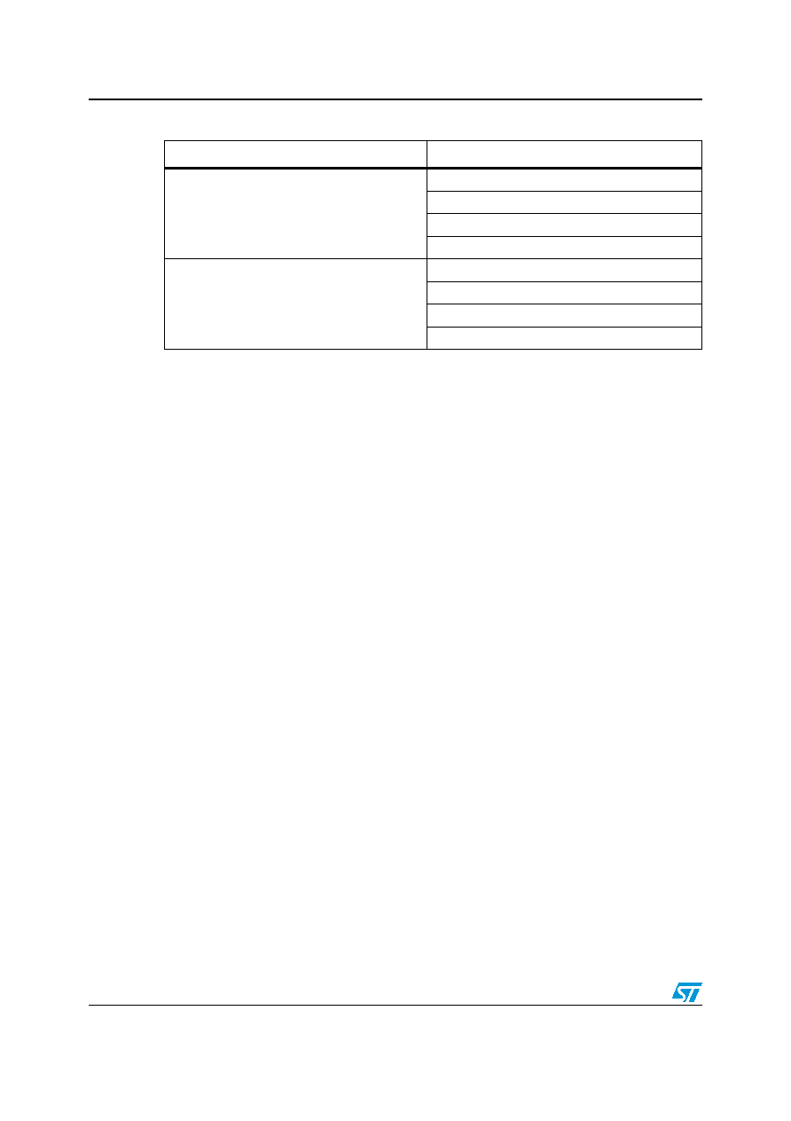
Table 1.
Product List
(1)
1.
x16 organization only available for MCP Products.
Reference
Part Number
NAND01G-B
NAND01GR3B
NAND01GW3B
NAND01GR4B
NAND01GW4B
NAND02G-B
NAND02GR3B
NAND02GW3B
NAND02GR4B
NAND02GW4B

NAND01G-B, NAND02G-B
Contents
3/64
Contents
1
Summary description . . . . . . . . . . . . . . . . . . . . . . . . . . . . . . . . . . . . . . . . 8
2
Memory array organization . . . . . . . . . . . . . . . . . . . . . . . . . . . . . . . . . . 15
2.1
Bad blocks . . . . . . . . . . . . . . . . . . . . . . . . . . . . . . . . . . . . . . . . . . . . . . . . 15
3
Signal descriptions . . . . . . . . . . . . . . . . . . . . . . . . . . . . . . . . . . . . . . . . . 17
3.1
Inputs/Outputs (I/O0-I/O7) . . . . . . . . . . . . . . . . . . . . . . . . . . . . . . . . . . . . 17
3.2
Inputs/Outputs (I/O8-I/O15) . . . . . . . . . . . . . . . . . . . . . . . . . . . . . . . . . . . 17
3.3
Address Latch Enable (AL) . . . . . . . . . . . . . . . . . . . . . . . . . . . . . . . . . . . 17
3.4
Command Latch Enable (CL) . . . . . . . . . . . . . . . . . . . . . . . . . . . . . . . . . . 17
3.5
Chip Enable (E) . . . . . . . . . . . . . . . . . . . . . . . . . . . . . . . . . . . . . . . . . . . . 17
3.6
Read Enable (R) . . . . . . . . . . . . . . . . . . . . . . . . . . . . . . . . . . . . . . . . . . . . 17
3.7
Power-Up Read Enable, Lock/Unlock Enable (PRL) . . . . . . . . . . . . . . . . 18
3.8
Write Enable (W) . . . . . . . . . . . . . . . . . . . . . . . . . . . . . . . . . . . . . . . . . . . 18
3.9
Write Protect (WP) . . . . . . . . . . . . . . . . . . . . . . . . . . . . . . . . . . . . . . . . . . 18
3.10
Ready/Busy (RB) . . . . . . . . . . . . . . . . . . . . . . . . . . . . . . . . . . . . . . . . . . . 18
3.11
V
DD
Supply Voltage . . . . . . . . . . . . . . . . . . . . . . . . . . . . . . . . . . . . . . . . . 18
3.12
V
SS
Ground . . . . . . . . . . . . . . . . . . . . . . . . . . . . . . . . . . . . . . . . . . . . . . . 19
4
Bus operations . . . . . . . . . . . . . . . . . . . . . . . . . . . . . . . . . . . . . . . . . . . . 19
4.1
Command Input . . . . . . . . . . . . . . . . . . . . . . . . . . . . . . . . . . . . . . . . . . . . 19
4.2
Address Input . . . . . . . . . . . . . . . . . . . . . . . . . . . . . . . . . . . . . . . . . . . . . . 19
4.3
Data Input . . . . . . . . . . . . . . . . . . . . . . . . . . . . . . . . . . . . . . . . . . . . . . . . . 19
4.4
Data Output . . . . . . . . . . . . . . . . . . . . . . . . . . . . . . . . . . . . . . . . . . . . . . . 20
4.5
Write Protect . . . . . . . . . . . . . . . . . . . . . . . . . . . . . . . . . . . . . . . . . . . . . . 20
4.6
Standby . . . . . . . . . . . . . . . . . . . . . . . . . . . . . . . . . . . . . . . . . . . . . . . . . . 20
5
Command Set . . . . . . . . . . . . . . . . . . . . . . . . . . . . . . . . . . . . . . . . . . . . . 22
6
Device operations . . . . . . . . . . . . . . . . . . . . . . . . . . . . . . . . . . . . . . . . . . 23
6.1
Read Memory Array . . . . . . . . . . . . . . . . . . . . . . . . . . . . . . . . . . . . . . . . . 23
6.1.1
Random Read . . . . . . . . . . . . . . . . . . . . . . . . . . . . . . . . . . . . . . . . . . . . 23

Contents
NAND01G-B, NAND02G-B
4/64
6.1.2
Page Read . . . . . . . . . . . . . . . . . . . . . . . . . . . . . . . . . . . . . . . . . . . . . . . 23
6.2
Cache Read . . . . . . . . . . . . . . . . . . . . . . . . . . . . . . . . . . . . . . . . . . . . . . . 26
6.3
Page Program . . . . . . . . . . . . . . . . . . . . . . . . . . . . . . . . . . . . . . . . . . . . . 27
6.3.1
Sequential Input . . . . . . . . . . . . . . . . . . . . . . . . . . . . . . . . . . . . . . . . . . . 27
6.3.2
Random Data Input . . . . . . . . . . . . . . . . . . . . . . . . . . . . . . . . . . . . . . . . 27
6.4
Copy Back Program . . . . . . . . . . . . . . . . . . . . . . . . . . . . . . . . . . . . . . . . . 29
6.5
Cache Program . . . . . . . . . . . . . . . . . . . . . . . . . . . . . . . . . . . . . . . . . . . . 31
6.6
Block Erase . . . . . . . . . . . . . . . . . . . . . . . . . . . . . . . . . . . . . . . . . . . . . . . 32
6.7
Reset . . . . . . . . . . . . . . . . . . . . . . . . . . . . . . . . . . . . . . . . . . . . . . . . . . . . 32
6.8
Read Status Register . . . . . . . . . . . . . . . . . . . . . . . . . . . . . . . . . . . . . . . . 33
6.8.1
Write Protection Bit (SR7) . . . . . . . . . . . . . . . . . . . . . . . . . . . . . . . . . . . 33
6.8.2
P/E/R Controller and Cache Ready/Busy Bit (SR6) . . . . . . . . . . . . . . . 33
6.8.3
P/E/R Controller Bit (SR5) . . . . . . . . . . . . . . . . . . . . . . . . . . . . . . . . . . . 33
6.8.4
Cache Program Error Bit (SR1) . . . . . . . . . . . . . . . . . . . . . . . . . . . . . . . 34
6.8.5
Error Bit (SR0) . . . . . . . . . . . . . . . . . . . . . . . . . . . . . . . . . . . . . . . . . . . . 34
6.8.6
SR4, SR3 and SR2 are Reserved . . . . . . . . . . . . . . . . . . . . . . . . . . . . . 34
6.9
Read Electronic Signature . . . . . . . . . . . . . . . . . . . . . . . . . . . . . . . . . . . . 35
7
Data protection . . . . . . . . . . . . . . . . . . . . . . . . . . . . . . . . . . . . . . . . . . . . 36
7.1
Blocks Lock . . . . . . . . . . . . . . . . . . . . . . . . . . . . . . . . . . . . . . . . . . . . . . . 36
7.2
Blocks Unlock . . . . . . . . . . . . . . . . . . . . . . . . . . . . . . . . . . . . . . . . . . . . . . 36
7.3
Blocks Lock-Down . . . . . . . . . . . . . . . . . . . . . . . . . . . . . . . . . . . . . . . . . . 37
7.4
Block Lock Status . . . . . . . . . . . . . . . . . . . . . . . . . . . . . . . . . . . . . . . . . . . 37
8
Software algorithms . . . . . . . . . . . . . . . . . . . . . . . . . . . . . . . . . . . . . . . . 40
8.1
Bad Block Management . . . . . . . . . . . . . . . . . . . . . . . . . . . . . . . . . . . . . . 40
8.2
Block Replacement . . . . . . . . . . . . . . . . . . . . . . . . . . . . . . . . . . . . . . . . . 40
8.3
Garbage Collection . . . . . . . . . . . . . . . . . . . . . . . . . . . . . . . . . . . . . . . . . . 42
8.4
Wear-leveling algorithm . . . . . . . . . . . . . . . . . . . . . . . . . . . . . . . . . . . . . . 42
8.5
Error Correction Code . . . . . . . . . . . . . . . . . . . . . . . . . . . . . . . . . . . . . . . 42
8.6
Hardware Simulation models . . . . . . . . . . . . . . . . . . . . . . . . . . . . . . . . . . 43
8.6.1
Behavioral simulation models . . . . . . . . . . . . . . . . . . . . . . . . . . . . . . . . 43
8.6.2
IBIS simulations models . . . . . . . . . . . . . . . . . . . . . . . . . . . . . . . . . . . . 43
9
Program and Erase Times and Endurance cycles . . . . . . . . . . . . . . . . 44

NAND01G-B, NAND02G-B
Contents
5/64
10
Maximum rating . . . . . . . . . . . . . . . . . . . . . . . . . . . . . . . . . . . . . . . . . . . . 45
11
DC And AC parameters . . . . . . . . . . . . . . . . . . . . . . . . . . . . . . . . . . . . . . 46
11.1
Ready/Busy Signal electrical characteristics . . . . . . . . . . . . . . . . . . . . . . 57
11.2
Data Protection . . . . . . . . . . . . . . . . . . . . . . . . . . . . . . . . . . . . . . . . . . . . . 58
12
Package mechanical . . . . . . . . . . . . . . . . . . . . . . . . . . . . . . . . . . . . . . . . 59
13
Part numbering . . . . . . . . . . . . . . . . . . . . . . . . . . . . . . . . . . . . . . . . . . . . 62
14
Revision history . . . . . . . . . . . . . . . . . . . . . . . . . . . . . . . . . . . . . . . . . . . 63

List of tables
NAND01G-B, NAND02G-B
6/64
List of tables
Table 1.
Product List . . . . . . . . . . . . . . . . . . . . . . . . . . . . . . . . . . . . . . . . . . . . . . . . . . . . . . . . . . . . . . 2
Table 2.
Product Description . . . . . . . . . . . . . . . . . . . . . . . . . . . . . . . . . . . . . . . . . . . . . . . . . . . . . . . 9
Table 3.
Signal Names . . . . . . . . . . . . . . . . . . . . . . . . . . . . . . . . . . . . . . . . . . . . . . . . . . . . . . . . . . . 11
Table 4.
Valid Blocks . . . . . . . . . . . . . . . . . . . . . . . . . . . . . . . . . . . . . . . . . . . . . . . . . . . . . . . . . . . . 15
Table 5.
Bus Operations . . . . . . . . . . . . . . . . . . . . . . . . . . . . . . . . . . . . . . . . . . . . . . . . . . . . . . . . . . 20
Table 6.
Address Insertion, x8 Devices . . . . . . . . . . . . . . . . . . . . . . . . . . . . . . . . . . . . . . . . . . . . . . 20
Table 7.
Address Insertion, x16 Devices . . . . . . . . . . . . . . . . . . . . . . . . . . . . . . . . . . . . . . . . . . . . . 21
Table 8.
Address Definitions, x8 . . . . . . . . . . . . . . . . . . . . . . . . . . . . . . . . . . . . . . . . . . . . . . . . . . . . 21
Table 9.
Address Definitions, x16 . . . . . . . . . . . . . . . . . . . . . . . . . . . . . . . . . . . . . . . . . . . . . . . . . . . 21
Table 10.
Commands . . . . . . . . . . . . . . . . . . . . . . . . . . . . . . . . . . . . . . . . . . . . . . . . . . . . . . . . . . . . . 22
Table 11.
Copy Back Program x8 Addresses . . . . . . . . . . . . . . . . . . . . . . . . . . . . . . . . . . . . . . . . . . . 29
Table 12.
Copy Back Program x16 Addresses . . . . . . . . . . . . . . . . . . . . . . . . . . . . . . . . . . . . . . . . . . 29
Table 13.
Status Register Bits . . . . . . . . . . . . . . . . . . . . . . . . . . . . . . . . . . . . . . . . . . . . . . . . . . . . . . 34
Table 14.
Electronic Signature . . . . . . . . . . . . . . . . . . . . . . . . . . . . . . . . . . . . . . . . . . . . . . . . . . . . . . 35
Table 15.
Electronic Signature Byte/Word 4 . . . . . . . . . . . . . . . . . . . . . . . . . . . . . . . . . . . . . . . . . . . . 35
Table 16.
Block Lock Status . . . . . . . . . . . . . . . . . . . . . . . . . . . . . . . . . . . . . . . . . . . . . . . . . . . . . . . . 38
Table 17.
Block Failure . . . . . . . . . . . . . . . . . . . . . . . . . . . . . . . . . . . . . . . . . . . . . . . . . . . . . . . . . . . . 41
Table 18.
Program, Erase Times and Program Erase Endurance Cycles . . . . . . . . . . . . . . . . . . . . . 44
Table 19.
Absolute Maximum Ratings . . . . . . . . . . . . . . . . . . . . . . . . . . . . . . . . . . . . . . . . . . . . . . . . 45
Table 20.
Operating and AC Measurement Conditions . . . . . . . . . . . . . . . . . . . . . . . . . . . . . . . . . . . 46
Table 21.
Capacitance . . . . . . . . . . . . . . . . . . . . . . . . . . . . . . . . . . . . . . . . . . . . . . . . . . . . . . . . . . . . 46
Table 22.
DC Characteristics, 1.8V Devices. . . . . . . . . . . . . . . . . . . . . . . . . . . . . . . . . . . . . . . . . . . . 47
Table 23.
DC Characteristics, 3V Devices . . . . . . . . . . . . . . . . . . . . . . . . . . . . . . . . . . . . . . . . . . . . . 48
Table 24.
AC Characteristics for Command, Address, Data Input . . . . . . . . . . . . . . . . . . . . . . . . . . . 49
Table 25.
AC Characteristics for Operations . . . . . . . . . . . . . . . . . . . . . . . . . . . . . . . . . . . . . . . . . . . 50
Table 26.
TSOP48 - 48 lead Plastic Thin Small Outline, 12 x 20 mm, Package Mechanical Data. . . 59
Table 27.
VFBGA63 9.5x12mm - 6x8 active ball array, 0.80mm pitch, Package Mechanical Data . . 60
Table 28.
TFBGA63 9.5x12mm - 6x8 active ball array, 0.80mm pitch, Package Mechanical Data . . 61
Table 29.
Ordering Information Scheme. . . . . . . . . . . . . . . . . . . . . . . . . . . . . . . . . . . . . . . . . . . . . . . 62
Table 30.
Document Revision History . . . . . . . . . . . . . . . . . . . . . . . . . . . . . . . . . . . . . . . . . . . . . . . . 63

NAND01G-B, NAND02G-B
List of figures
7/64
List of figures
Figure 1.
Logic Block Diagram . . . . . . . . . . . . . . . . . . . . . . . . . . . . . . . . . . . . . . . . . . . . . . . . . . . . . . 10
Figure 2.
Logic Diagram. . . . . . . . . . . . . . . . . . . . . . . . . . . . . . . . . . . . . . . . . . . . . . . . . . . . . . . . . . . 10
Figure 3.
TSOP48 Connections, x8 devices . . . . . . . . . . . . . . . . . . . . . . . . . . . . . . . . . . . . . . . . . . . 12
Figure 4.
FBGA63 Connections, x8 devices (Top view through package). . . . . . . . . . . . . . . . . . . . . 13
Figure 5.
FBGA63 Connections, x16 devices (Top view through package). . . . . . . . . . . . . . . . . . . . 14
Figure 6.
Memory Array Organization . . . . . . . . . . . . . . . . . . . . . . . . . . . . . . . . . . . . . . . . . . . . . . . . 16
Figure 7.
Read Operations. . . . . . . . . . . . . . . . . . . . . . . . . . . . . . . . . . . . . . . . . . . . . . . . . . . . . . . . . 24
Figure 8.
Random Data Output During Sequential Data Output . . . . . . . . . . . . . . . . . . . . . . . . . . . . 25
Figure 9.
Cache Read Operation . . . . . . . . . . . . . . . . . . . . . . . . . . . . . . . . . . . . . . . . . . . . . . . . . . . . 26
Figure 10.
Page Program Operation . . . . . . . . . . . . . . . . . . . . . . . . . . . . . . . . . . . . . . . . . . . . . . . . . . 28
Figure 11.
Random Data Input During Sequential Data Input . . . . . . . . . . . . . . . . . . . . . . . . . . . . . . . 28
Figure 12.
Copy Back Program . . . . . . . . . . . . . . . . . . . . . . . . . . . . . . . . . . . . . . . . . . . . . . . . . . . . . . 30
Figure 13.
Page Copy Back Program with Random Data Input. . . . . . . . . . . . . . . . . . . . . . . . . . . . . . 30
Figure 14.
Cache Program Operation . . . . . . . . . . . . . . . . . . . . . . . . . . . . . . . . . . . . . . . . . . . . . . . . . 31
Figure 15.
Block Erase Operation . . . . . . . . . . . . . . . . . . . . . . . . . . . . . . . . . . . . . . . . . . . . . . . . . . . . 32
Figure 16.
Blocks Unlock Operation . . . . . . . . . . . . . . . . . . . . . . . . . . . . . . . . . . . . . . . . . . . . . . . . . . 37
Figure 17.
Read Block Lock Status Operation . . . . . . . . . . . . . . . . . . . . . . . . . . . . . . . . . . . . . . . . . . . 38
Figure 18.
Block Protection State Diagram . . . . . . . . . . . . . . . . . . . . . . . . . . . . . . . . . . . . . . . . . . . . . 39
Figure 19.
Bad Block Management Flowchart . . . . . . . . . . . . . . . . . . . . . . . . . . . . . . . . . . . . . . . . . . . 41
Figure 20.
Garbage Collection . . . . . . . . . . . . . . . . . . . . . . . . . . . . . . . . . . . . . . . . . . . . . . . . . . . . . . . 41
Figure 21.
Error Detection . . . . . . . . . . . . . . . . . . . . . . . . . . . . . . . . . . . . . . . . . . . . . . . . . . . . . . . . . . 43
Figure 22.
Equivalent Testing Circuit for AC Characteristics Measurement . . . . . . . . . . . . . . . . . . . . 47
Figure 23.
Command Latch AC Waveforms . . . . . . . . . . . . . . . . . . . . . . . . . . . . . . . . . . . . . . . . . . . . 51
Figure 24.
Address Latch AC Waveforms . . . . . . . . . . . . . . . . . . . . . . . . . . . . . . . . . . . . . . . . . . . . . . 51
Figure 25.
Data Input Latch AC Waveforms . . . . . . . . . . . . . . . . . . . . . . . . . . . . . . . . . . . . . . . . . . . . 52
Figure 26.
Sequential Data Output after Read AC Waveforms . . . . . . . . . . . . . . . . . . . . . . . . . . . . . . 52
Figure 27.
Read Status Register AC Waveform . . . . . . . . . . . . . . . . . . . . . . . . . . . . . . . . . . . . . . . . . 53
Figure 28.
Read Electronic Signature AC Waveform. . . . . . . . . . . . . . . . . . . . . . . . . . . . . . . . . . . . . . 53
Figure 29.
Page Read Operation AC Waveform . . . . . . . . . . . . . . . . . . . . . . . . . . . . . . . . . . . . . . . . . 54
Figure 30.
Page Program AC Waveform . . . . . . . . . . . . . . . . . . . . . . . . . . . . . . . . . . . . . . . . . . . . . . . 55
Figure 31.
Block Erase AC Waveform . . . . . . . . . . . . . . . . . . . . . . . . . . . . . . . . . . . . . . . . . . . . . . . . . 56
Figure 32.
Reset AC Waveform . . . . . . . . . . . . . . . . . . . . . . . . . . . . . . . . . . . . . . . . . . . . . . . . . . . . . . 56
Figure 33.
Ready/Busy AC Waveform . . . . . . . . . . . . . . . . . . . . . . . . . . . . . . . . . . . . . . . . . . . . . . . . . 57
Figure 34.
Ready/Busy Load Circuit . . . . . . . . . . . . . . . . . . . . . . . . . . . . . . . . . . . . . . . . . . . . . . . . . . 57
Figure 35.
Resistor Value Versus Waveform Timings For Ready/Busy Signal . . . . . . . . . . . . . . . . . . 58
Figure 36.
Data Protection . . . . . . . . . . . . . . . . . . . . . . . . . . . . . . . . . . . . . . . . . . . . . . . . . . . . . . . . . 58
Figure 37.
TSOP48 - 48 lead Plastic Thin Small Outline, 12 x 20 mm, Package Outline . . . . . . . . . . 59
Figure 38.
VFBGA63 9.5x12mm - 6x8 active ball array, 0.80mm pitch, Package Outline. . . . . . . . . . 60
Figure 39.
TFBGA63 9.5x12mm - 6x8 active ball array, 0.80mm pitch, Package Outline . . . . . . . . . . 61

Summary description
NAND01G-B, NAND02G-B
8/64
1 Summary
description
The NAND Flash 2112 Byte/ 1056 Word Page is a family of non-volatile Flash memories
that uses NAND cell technology. The devices range from 1 Gbit to 2 Gbits and operate with
either a 1.8V or 3V voltage supply. The size of a Page is either 2112 Bytes (2048 + 64
spare) or 1056 Words (1024 + 32 spare) depending on whether the device has a x8 or x16
bus width.
The address lines are multiplexed with the Data Input/Output signals on a multiplexed x8 or
x16 Input/Output bus. This interface reduces the pin count and makes it possible to migrate
to other densities without changing the footprint.
Each block can be programmed and erased over 100,000 cycles. To extend the lifetime of
NAND Flash devices it is strongly recommended to implement an Error Correction Code
(ECC).
The devices have hardware and software security features:
A Write Protect pin is available to give a hardware protection against program and
erase operations.
A Block Locking scheme is available to provide user code and/or data protection.
The devices feature an open-drain Ready/Busy output that can be used to identify if the
Program/Erase/Read (P/E/R) Controller is currently active. The use of an open-drain output
allows the Ready/Busy pins from several memories to be connected to a single pull-up
resistor.
A Copy Back Program command is available to optimize the management of defective
blocks. When a Page Program operation fails, the data can be programmed in another page
without having to resend the data to be programmed.
Each device has Cache Program and Cache Read features which improve the program and
read throughputs for large files. During Cache Programming, the device loads the data in a
Cache Register while the previous data is transferred to the Page Buffer and programmed
into the memory array. During Cache Reading, the device loads the data in a Cache
Register while the previous data is transferred to the I/O Buffers to be read.
All devices have the Chip Enable Don't Care feature, which allows code to be directly
downloaded by a microcontroller, as Chip Enable transitions during the latency time do not
stop the read operation.
All devices have the option of a Unique Identifier (serial number), which allows each device
to be uniquely identified.
The Unique Identifier options is subject to an NDA (Non Disclosure Agreement) and so not
described in the datasheet. For more details of this option contact your nearest ST Sales
office.
The devices are available in the following packages:
TSOP48 (12 x 20mm) for all products
VFBGA63 (9.5 x 12 x 1mm, 0.8mm pitch) for 1Gb products
TFBGA63 (9.5 x 12 x 1.2mm, 0.8mm pitch) for 2Gb Dual Die products
In order to meet environmental requirements, ST offers the NAND01G-B and NAND02G-B
in ECOPACK
Æ
packages. ECOPACK packages are Lead-free. The category of second Level
Interconnect is marked on the package and on the inner box label, in compliance with

NAND01G-B, NAND02G-B
Summary description
9/64
JEDEC Standard JESD97. The maximum ratings related to soldering conditions are also
marked on the inner box label. ECOPACK is an ST trademark.
For information on how to order these options refer to
Table 29: Ordering Information
Scheme
. Devices are shipped from the factory with Block 0 always valid and the memory
content bits, in valid blocks, erased to '1'.
See
Table 2: Product Description
, for all the devices available in the family.
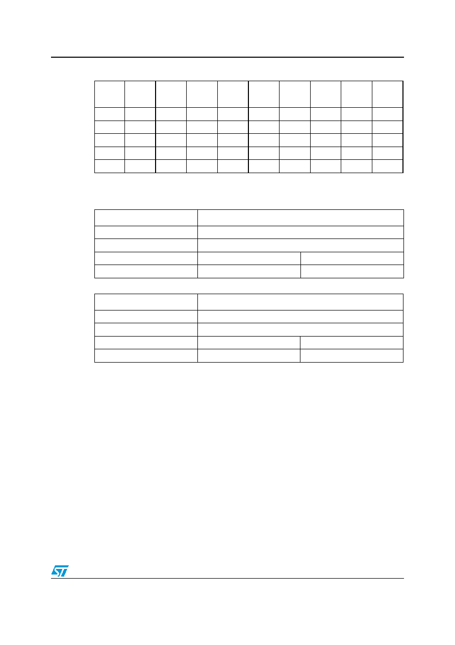
Table 2.
Product Description
(1)
Reference
Part Number
Density
Bus
Width
Page
Size
Block
Size
Memory
Array
Operating
Voltage
Timings
Packages
Random
access
time
(max)
Sequential
access
time
(min)
Page
Program
time
(typ)
Block
Erase
(typ)
NAND01G
-B
NAND01GR3B
1Gbit
x8
2048+
64
Bytes
128K+
4K
Bytes
64
Pages x
1024
Blocks
1.7 to
1.95V
25µs
60ns
300µs
2ms
TSOP48
VFBGA63
NAND01GW3B
2.7 to
3.6V
25µs
50ns
300µs
NAND01GR4B
x16
(2)
1024+
32
Words
64K+
2K
Words
1.7 to
1.95V
25µs
60ns
300µs
NAND01GW4B
2.7 to
3.6V
25µs
50ns
300µs
NAND02G
-B
NAND02GR3B
2Gbit
x8
2048+
64
Bytes
128K+
4K
Bytes
64
Pages x
2048
Blocks
1.7 to
1.95V
25µs
60ns
300µs
2ms
TSOP48
TFBGA63
(2)
NAND02GW3B
2.7 to
3.6V
25µs
50ns
300µs
NAND02GR4B
x16
(2)
1024+
32
Words
64K+
2K
Words
1.7 to
1.95V
25µs
60ns
300µs
NAND02GW4B
2.7 to
3.6V
25µs
50ns
300µs
1.
x16 organization only available for MCP
2.
Dual Die devices only
Summary description
NAND01G-B, NAND02G-B
10/64
Figure 1.
Logic Block Diagram
Figure 2.
Logic Diagram
1.
x16 organization only available for MCP
Address
Register/Counter
Command
Interface
Logic
P/E/R Controller,
High Voltage
Generator
WP
I/O Buffers & Latches
I/O8-I/O15, x16
E
W
AI09373b
R
Y Decoder
Page Buffer
NAND Flash
Memory Array
X Decoder
I/O0-I/O7, x8/x16
Command Register
CL
AL
Cache Register
RB
PRL
AI09372b
W
I/O8-I/O15, x16
VDD
NAND Flash
E
VSS
WP
AL
CL
RB
R
I/O0-I/O7, x8/x16
PRL
NAND01G-B, NAND02G-B
Summary description
11/64
Table 3.
Signal Names
I/O8-15
Data Input/Outputs for x16 devices
I/O0-7
Data Input/Outputs, Address Inputs, or Command Inputs for x8 and
x16 devices
AL
Address Latch Enable
CL
Command Latch Enable
E
Chip Enable
R
Read Enable
RB
Ready/Busy (open-drain output)
W
Write Enable
WP
Write Protect
PRL
Power-Up Read Enable, Lock/Unlock Enable
V
DD
Supply Voltage
V
SS
Ground
NC
Not Connected Internally
DU
Do Not Use
Summary description
NAND01G-B, NAND02G-B
12/64
Figure 3.
TSOP48 Connections, x8 devices
I/O3
I/O2
I/O6
R
RB
NC
I/O4
I/O7
AI11750
NAND Flash
(x8)
12
1
13
24
25
36
37
48
E
I/O1
NC
NC
NC
NC
NC
NC
NC
WP
W
NC
NC
NC
VSS
VDD
AL
NC
NC
CL
NC
I/O5
NC
NC
NC
I/O0
NC
NC
NC
NC
PRL
VDD
NC
NC
NC
VSS
NC
NC
NC
NC
NAND01G-B, NAND02G-B
Summary description
13/64
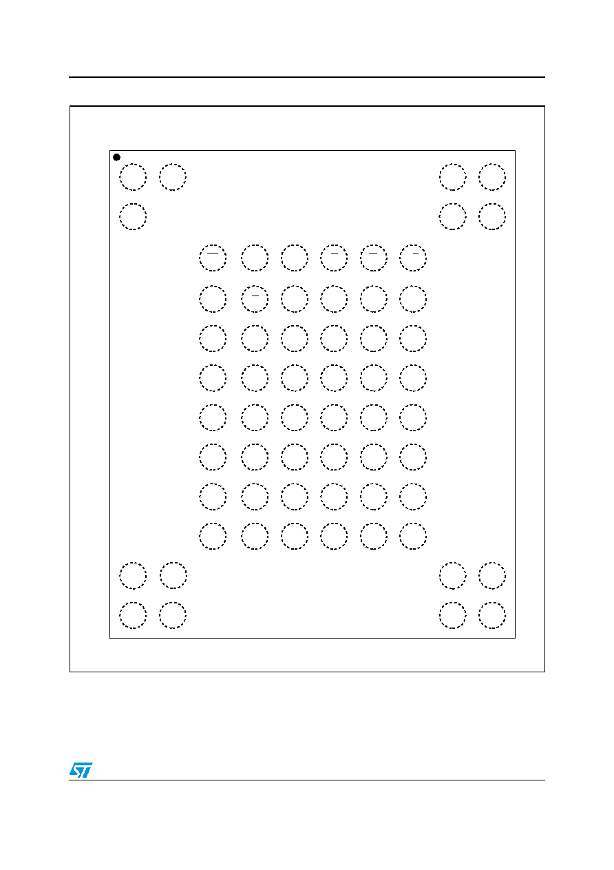
Figure 4.
FBGA63 Connections, x8 devices (Top view through package)
AI09376
I/O7
WP
I/O4
I/O3
NC
VDD
I/O5
VDD
NC
H
VSS
I/O6
D
E
CL
C
NC
NC
B
DU
NC
W
NC
A
8
7
6
5
4
3
2
1
NC
NC
NC
NC
G
F
E
I/O0
AL
DU
NC
NC
NC
NC
NC
NC
NC
NC
NC
NC
VSS
NC
NC
NC
NC
RB
I/O2
DU
NC
DU
I/O1
10
9
R
NC
PRL
NC
VSS
DU
DU
DU
DU
DU
DU
DU
DU
DU
DU
DU
M
L
K
J

Summary description
NAND01G-B, NAND02G-B
14/64
Figure 5.
FBGA63 Connections, x16 devices (Top view through package)
AI09377
I/O15
WP
I/O4
I/O11
I/O10
VDD
I/O6
VDD
I/O3
H
VSS
I/O13
D
E
CL
C
NC
NC
B
DU
NC
W
NC
A
8
7
6
5
4
3
2
1
NC
NC
NC
NC
G
F
E
I/O1
AL
DU
NC
NC
NC
NC
NC
NC
I/O7
I/O5
I/O14
I/O12
VSS
NC
NC
NC
NC
RB
I/O2
DU
I/O0
DU
I/O9
10
9
R
NC
PRL
I/O8
VSS
DU
DU
DU
DU
DU
DU
DU
DU
DU
DU
DU
M
L
K
J
NAND01G-B, NAND02G-B
Memory array organization
15/64
2
Memory array organization
The memory array is made up of NAND structures where 32 cells are connected in series.
The memory array is organized in blocks where each block contains 64 pages. The array is
split into two areas, the main area and the spare area. The main area of the array is used to
store data whereas the spare area is typically used to store Error correction Codes, software
flags or Bad Block identification.
In x8 devices the pages are split into a 2048 Byte main area and a spare area of 64 Bytes.
In the x16 devices the pages are split into a 1,024 Word main area and a 32 Word spare
area. Refer to
Figure 6: Memory Array Organization
.
2.1 Bad
blocks
The NAND Flash 2112 Byte/ 1056 Word Page devices may contain Bad Blocks, that is
blocks that contain one or more invalid bits whose reliability is not guaranteed. Additional
Bad Blocks may develop during the lifetime of the device.
The Bad Block Information is written prior to shipping (refer to
Section 8.1: Bad Block
Management
for more details).
Table 4: Valid Blocks
shows the minimum number of valid blocks in each device. The values
shown include both the Bad Blocks that are present when the device is shipped and the Bad
Blocks that could develop later on.
These blocks need to be managed using Bad Blocks Management, Block Replacement or
Error Correction Codes (refer to
Section 8: Software algorithms
).
Table 4.
Valid Blocks
Density of Device
Min
Max
2 Gbits
2008
2048
1 Gbit
1004
1024
Memory array organization
NAND01G-B, NAND02G-B
16/64
Figure 6.
Memory Array Organization
AI09854
Block = 64 Pages
Page = 2112 Bytes (2,048 + 64)
2,048 Bytes
2048 Bytes
Spare Area
64
Bytes
Block
8 bits
64
Bytes
8 bits
Page
Page Buffer, 2112 Bytes
Block = 64 Pages
Page = 1056 Words (1024 + 32)
1,024 Words
1024 Words
Spare Area
Main Area
32
Words
16 bits
32
Words
16 bits
Page Buffer, 1056 Words
Block
Page
x8 DEVICES
x16 DEVICES
Main Area

NAND01G-B, NAND02G-B
Signal descriptions
17/64
3 Signal
descriptions
See
Figure 2: Logic Diagram
, and
Table 3: Signal Names
, for a brief overview of the signals
connected to this device.
3.1 Inputs/Outputs
(I/O0-I/O7)
Input/Outputs 0 to 7 are used to input the selected address, output the data during a Read
operation or input a command or data during a Write operation. The inputs are latched on
the rising edge of Write Enable. I/O0-I/O7 are left floating when the device is deselected or
the outputs are disabled.
3.2 Inputs/Outputs
(I/O8-I/O15)
Input/Outputs 8 to 15 are only available in x16 devices. They are used to output the data
during a Read operation or input data during a Write operation. Command and Address
Inputs only require I/O0 to I/O7.
The inputs are latched on the rising edge of Write Enable. I/O8-I/O15 are left floating when
the device is deselected or the outputs are disabled.
3.3
Address Latch Enable (AL)
The Address Latch Enable activates the latching of the Address inputs in the Command
Interface. When AL is high, the inputs are latched on the rising edge of Write Enable.
3.4
Command Latch Enable (CL)
The Command Latch Enable activates the latching of the Command inputs in the Command
Interface. When CL is high, the inputs are latched on the rising edge of Write Enable.
3.5 Chip
Enable
(E)
The Chip Enable input activates the memory control logic, input buffers, decoders and
sense amplifiers. When Chip Enable is low, V
IL
, the device is selected. If Chip Enable goes
high, v
IH
, while the device is busy, the device remains selected and does not go into standby
mode.
3.6 Read
Enable
(R)
The Read Enable pin, R, controls the sequential data output during Read operations. Data
is valid t
RLQV
after the falling edge of R. The falling edge of R also increments the internal
column address counter by one.

Signal descriptions
NAND01G-B, NAND02G-B
18/64
3.7
Power-Up Read Enable, Lock/Unlock Enable (PRL)
The Power-Up Read Enable, Lock/Unlock Enable input, PRL, is used to enable and disable
the lock mechanism. When PRL is High, V
IH
, the device is in Block Lock mode.
If the Power-Up Read Enable, Lock/Unlock Enable input is not required, the PRL pin should
be left unconnected (Not Connected) or connected to V
SS
.
3.8 Write
Enable
(W)
The Write Enable input, W, controls writing to the Command Interface, Input Address and
Data latches. Both addresses and data are latched on the rising edge of Write Enable.
During power-up and power-down a recovery time of 10µs (min) is required before the
Command Interface is ready to accept a command. It is recommended to keep Write Enable
high during the recovery time.
3.9
Write Protect (WP)
The Write Protect pin is an input that gives a hardware protection against unwanted program
or erase operations. When Write Protect is Low, V
IL
, the device does not accept any
program or erase operations.
It is recommended to keep the Write Protect pin Low, V
IL
, during power-up and power-down.
3.10 Ready/Busy
(RB)
The Ready/Busy output, RB, is an open-drain output that can be used to identify if the P/E/R
Controller is currently active. When Ready/Busy is Low, V
OL
, a read, program or erase
operation is in progress. When the operation completes Ready/Busy goes High, V
OH
.
The use of an open-drain output allows the Ready/Busy pins from several memories to be
connected to a single pull-up resistor. A Low will then indicate that one, or more, of the
memories is busy.
Refer to the
Section 11.1: Ready/Busy Signal electrical characteristics
for details on how to
calculate the value of the pull-up resistor.
3.11 V
DD
Supply Voltage
V
DD
provides the power supply to the internal core of the memory device. It is the main
power supply for all operations (read, program and erase).
An internal voltage detector disables all functions whenever V
DD
is below V
LKO
(see
Table 22
and
Table 23
) or 1.5V (for 1.8V devices) to protect the device from any involuntary
program/erase during power-transitions.
Each device in a system should have V
DD
decoupled with a 0.1µF capacitor. The PCB track
widths should be sufficient to carry the required program and erase currents.

NAND01G-B, NAND02G-B
Bus operations
19/64
3.12 V
SS
Ground
Ground, V
SS,
is the reference for the power supply. It must be connected to the system
ground.
4 Bus
operations
There are six standard bus operations that control the memory. Each of these is described
in this section, see
Table 5: Bus Operations
, for a summary.
Typically, glitches of less than 5 ns on Chip Enable, Write Enable and Read Enable are
ignored by the memory and do not affect bus operations.
4.1 Command
Input
Command Input bus operations are used to give commands to the memory. Commands are
accepted when Chip Enable is Low, Command Latch Enable is High, Address Latch Enable
is Low and Read Enable is High. They are latched on the rising edge of the Write Enable
signal.
Only I/O0 to I/O7 are used to input commands.
See
Figure 23
and
Table 24
for details of the timings requirements.
4.2 Address
Input
Address Input bus operations are used to input the memory addresses. Four bus cycles are
required to input the addresses for 1Gb devices whereas five bus cycles are required for the
2Gb device (refer to
Table 6
and
Table 7
, Address Insertion).
The addresses are accepted when Chip Enable is Low, Address Latch Enable is High,
Command Latch Enable is Low and Read Enable is High. They are latched on the rising
edge of the Write Enable signal. Only I/O0 to I/O7 are used to input addresses.
See
Figure 24
and
Table 24
for details of the timings requirements.
4.3 Data
Input
Data Input bus operations are used to input the data to be programmed.
Data is accepted only when Chip Enable is Low, Address Latch Enable is Low, Command
Latch Enable is Low and Read Enable is High. The data is latched on the rising edge of the
Write Enable signal. The data is input sequentially using the Write Enable signal.
See
Figure 25
and
Table 24
and
Table 25
for details of the timings requirements.
Bus operations
NAND01G-B, NAND02G-B
20/64
4.4 Data
Output
Data Output bus operations are used to read: the data in the memory array, the Status
Register, the lock status, the Electronic Signature
and the Unique Identifier.
Data is output when Chip Enable is Low, Write Enable is High, Address Latch Enable is Low,
and Command Latch Enable is Low. The data is output sequentially using the Read Enable
signal.
See
Figure 26
and
Table 25
for details of the timings requirements.
4.5 Write
Protect
Write Protect bus operations are used to protect the memory against program or erase
operations. When the Write Protect signal is Low the device will not accept program or erase
operations and so the contents of the memory array cannot be altered. The Write Protect
signal is not latched by Write Enable to ensure protection even during power-up.
4.6 Standby
When Chip Enable is High the memory enters Standby mode, the device is deselected,
outputs are disabled and power consumption is reduced.
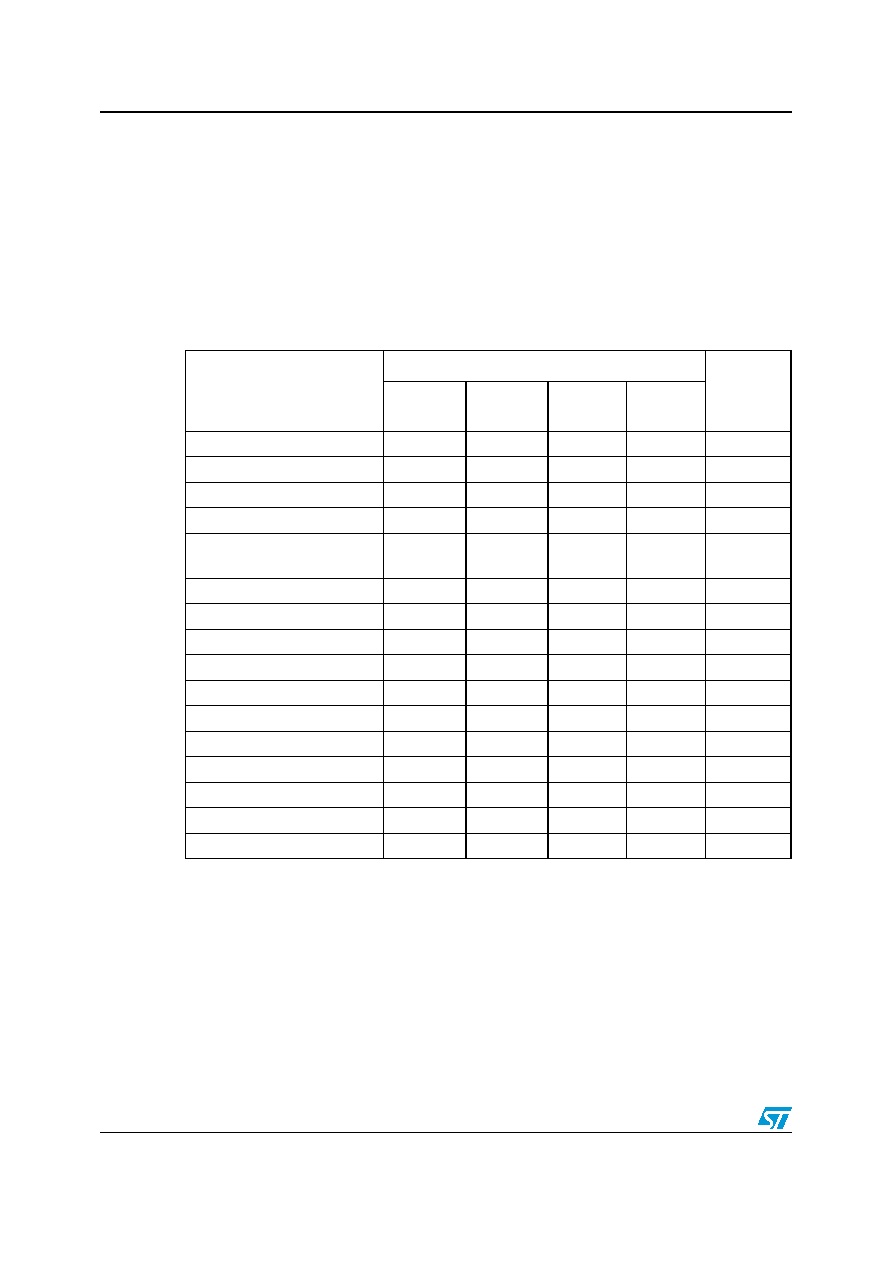
Table 5.
Bus Operations
Bus Operation
E
AL
CL
R
W
WP
I/O0 - I/O7
I/O8 - I/O15
(1)
1. Only for x16 devices.
Command Input
V
IL
V
IL
V
IH
V
IH
Rising
X
(2)
2. WP must be V
IH
when issuing a program or erase command.
Command
X
Address Input
V
IL
V
IH
V
IL
V
IH
Rising
X
Address
X
Data Input
V
IL
V
IL
V
IL
V
IH
Rising
V
IH
Data Input
Data Input
Data Output
V
IL
V
IL
V
IL
Fallin
g
V
IH
X
Data Output
Data Output
Write Protect
X
X
X
X
X
V
IL
X
X
Standby
V
IH
X
X
X
X
V
IL
/V
D
D
X
X
Table 6.
Address Insertion, x8 Devices
Bus Cycle
(1)
1.
Any additional address input cycles will be ignored.
I/O7
I/O6
I/O5
I/O4
I/O3
I/O2
I/O1
I/O0
1
st
A7
A6
A5
A4
A3
A2
A1
A0
2
nd
V
IL
V
IL
V
IL
V
IL
A11
A10
A9
A8
3
rd
A19
A18
A17
A16
A15
A14
A13
A12
4
th
A27
A26
A25
A24
A23
A22
A21
A20
5
th(2)
2.
The fifth cycle is valid for 2Gb devices. A28 is for 2Gb devices only.
V
IL
V
IL
V
IL
V
IL
V
IL
V
IL
V
IL
A28
NAND01G-B, NAND02G-B
Bus operations
21/64
Table 7.
Address Insertion, x16 Devices
Bus
Cycle
(1)
1.
Any additional address input cycles will be ignored.
I/O8-
I/O15
I/O7
I/O6
I/O5
I/O4
I/O3
I/O2
I/O1
I/O0
1
st
X
A7
A6
A5
A4
A3
A2
A1
A0
2
nd
X
V
IL
V
IL
V
IL
V
IL
V
IL
A10
A9
A8
3
rd
X
A18
A17
A16
A15
A14
A13
A12
A11
4
th
X
A26
A25
A24
A23
A22
A21
A20
A19
5
th(2)
2.
The fifth cycle is valid for 2Gb devices. A27 is for 2Gb devices only.
X
V
IL
V
IL
V
IL
V
IL
V
IL
V
IL
V
IL
A27
Table 8.
Address Definitions, x8
Address
Definition
A0 - A11
Column Address
A12 - A17
Page Address
A18 - A27
Block Address
1Gb device
A18 - A28
Block Address
2Gb device
Table 9.
Address Definitions, x16
Address
Definition
A0 - A10
Column Address
A11 - A16
Page Address
A17 - A26
Block Address
1Gb device
A17 - A27
Block Address
2Gb device
Command Set
NAND01G-B, NAND02G-B
22/64
5 Command
Set
All bus write operations to the device are interpreted by the Command Interface. The
Commands are input on I/O0-I/O7 and are latched on the rising edge of Write Enable when
the Command Latch Enable signal is high. Device operations are selected by writing
specific commands to the Command Register. The two-step command sequences for
program and erase operations are imposed to maximize data security.
The Commands are summarized in
Table 10: Commands
.
Table 10.
Commands
Command
Bus Write Operations
(1)(2)
1. The bus cycles are only shown for issuing the codes. The cycles required to input the
addresses or input/output data are not shown.
2. For consecutive Read operations the 00h command does not need to be repeated.
Commands
accepted
during
busy
1
st
CYCLE
2
nd
CYCLE 3
rd
CYCLE 4
th
CYCLE
Read
00h
(2)
30h
≠
≠
Random Data Output
05h
E0h
≠
≠
Cache Read
00h
31h
≠
≠
Exit Cache Read
34h
≠
≠
≠
Yes
(3)
3. Only during Cache Read busy.
Page Program
(Sequential Input default)
80h
10h
≠
≠
Random Data Input
85h
≠
≠
≠
Copy Back Program
00h
35h
85h
10h
Cache Program
80h
15h
≠
≠
Block Erase
60h
D0h
≠
≠
Reset
FFh
≠
≠
≠
Yes
Read Electronic Signature
90h
≠
≠
≠
Read Status Register
70h
≠
≠
≠
Yes
Read Block Lock Status
7Ah
≠
≠
≠
Blocks Unlock
23h
24h
≠
≠
Blocks Lock
2Ah
≠
≠
≠
Blocks Lock-Down
2Ch
≠
≠
≠

NAND01G-B, NAND02G-B
Device operations
23/64
6 Device
operations
The following section gives the details of the device operations.
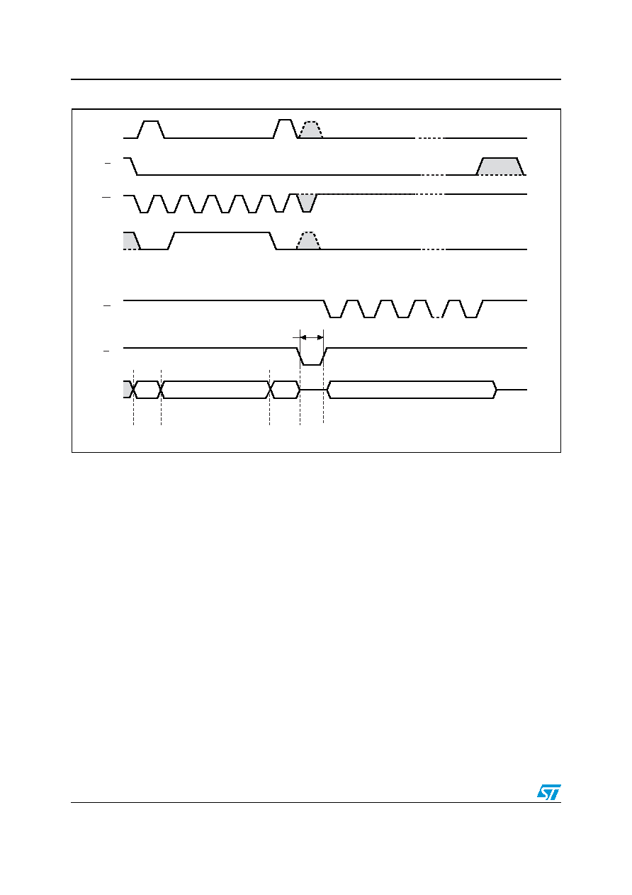
6.1 Read
Memory
Array
At Power-Up the device defaults to Read mode. To enter Read mode from another mode the
Read command must be issued, see
Table 10: Commands
. Once a Read command is
issued, subsequent consecutive Read commands only require the confirm command code
(30h).
Once a Read command is issued two types of operations are available: Random Read and
Page Read.
6.1.1 Random
Read
Each time the Read command is issued the first read is Random Read.
6.1.2 Page
Read
After the first Random Read access, the page data (2112 Bytes or 1056 Words) is
transferred to the Page Buffer in a time of t
WHBH
(refer to
Table 25
for value). Once the
transfer is complete the Ready/Busy signal goes High. The data can then be read out
sequentially (from selected column address to last column address) by pulsing the Read
Enable signal.
The device can output random data in a page, instead of the consecutive sequential data, by
issuing a Random Data Output command.
The Random Data Output command can be used to skip some data during a sequential
data output.
The sequential operation can be resumed by changing the column address of the next data
to be output, to the address which follows the Random Data Output command.
The Random Data Output command can be issued as many times as required within a
page.
The Random Data Output command is not accepted during Cache Read operations.
Device operations
NAND01G-B, NAND02G-B
24/64
Figure 7.
Read Operations
1.
Highest address depends on device density.
CL
E
W
AL
R
I/O
RB
00h
ai08657b
Busy
Command
Code
Data Output (sequentially)
Address Input
tBLBH1
30h
Command
Code
NAND01G-B, NAND02G-B
Device operations
25/64
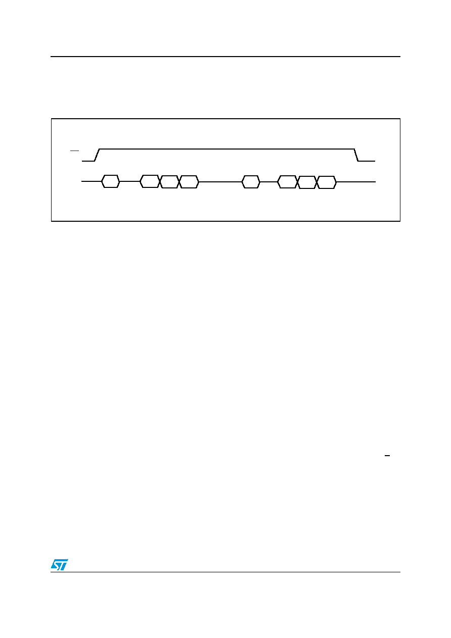
Figure 8.
Random Data Output During Sequential Data Output
I/O
RB
Address
Inputs
ai08658
Data Output
Busy
tBLBH1
(Read Busy time)
00h
Cmd
Code
30h
Address
Inputs
Data Output
05h
E0h
5 Add cycles
Main Area
Spare
Area
Col Add 1,2
Row Add 1,2,3
Cmd
Code
Cmd
Code
Cmd
Code
2Add cycles
Main Area
Spare
Area
Col Add 1,2
R
Device operations
NAND01G-B, NAND02G-B
26/64
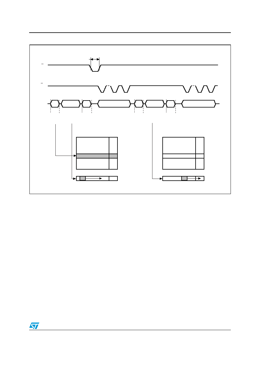
6.2 Cache
Read
The Cache Read operation is used to improve the read throughput by reading data using
the Cache Register. As soon as the user starts to read one page, the device automatically
loads the next page into the Cache Register.
An Cache Read operation consists of three steps (see
Table 10: Commands
):
1.
One bus cycle is required to setup the Cache Read command (the same as the
standard Read command)
2.
Four or Five (refer to
Table 6
and
Table 7
) bus cycles are then required to input the
Start Address
3.
One bus cycle is required to issue the Cache Read confirm command to start the P/E/R
Controller.
The Start Address must be at the beginning of a page (Column Address = 00h, see
Table 8
and
Table 9
). This allows the data to be output uninterrupted after the latency time (t
BLBH1
),
see
Figure 9
The Ready/Busy signal can be used to monitor the start of the operation. During the latency
period the Ready/Busy signal goes Low, after this the Ready/Busy signal goes High, even if
the device is internally downloading page n+1.
Once the Cache Read operation has started, the Status Register can be read using the
Read Status Register command.
During the operation, SR5 can be read, to find out whether the internal reading is ongoing
(SR5 = `0'), or has completed (SR5 = `1'), while SR6 indicates whether the Cache Register
is ready to download new data.
To exit the Cache Read operation an Exit Cache Read command must be issued (see
Table 10
).
If the Exit Cache Read command is issued while the device is internally reading page n+1,
page n will still be output, but not page n+1.
Figure 9.
Cache Read Operation
I/O
RB
Address
Inputs
ai08661
00h
Read
Setup
Code
31h
Cache
Read
Confirm
Code
Busy
tBLBH1
(Read Busy time)
1st page
Data Output
2nd page
3rd page
last page
34h
Exit
Cache
Read
Code
Block N

NAND01G-B, NAND02G-B
Device operations
27/64
6.3 Page
Program
The Page Program operation is the standard operation to program data to the memory
array. Generally, data is programmed sequentially, however the device does support
Random Input within a page.
The memory array is programmed by page, however partial page programming is allowed
where any number of Bytes (1 to 2112) or Words (1 to 1056) can be programmed.
The maximum number of consecutive partial page program operations allowed in the same
page is eight. After exceeding this a Block Erase command must be issued before any
further program operations can take place in that page.
6.3.1 Sequential
Input
To input data sequentially the addresses must be sequential and remain in one block.
For Sequential Input each Page Program operation consists of five steps (see
Figure 10
):
1.
one bus cycle is required to setup the Page Program (Sequential Input) command (see
Table 10
)
2.
four or five bus cycles are then required to input the program address (refer to
Table 6
and
Table 7
)
3.
the data is then loaded into the Data Registers
4.
one bus cycle is required to issue the Page Program confirm command to start the
P/E/R Controller. The P/E/R will only start if the data has been loaded in step 3.
5.
the P/E/R Controller then programs the data into the array.
6.3.2
Random Data Input
During a Sequential Input operation, the next sequential address to be programmed can be
replaced by a random address, by issuing a Random Data Input command. The following
two steps are required to issue the command:
1.
one bus cycle is required to setup the Random Data Input command (see
Table 10
)
2.
two bus cycles are then required to input the new column address (refer to
Table 6
)
Random Data Input can be repeated as often as required in any given page.
Once the program operation has started the Status Register can be read using the Read
Status Register command. During program operations the Status Register will only flag
errors for bits set to '1' that have not been successfully programmed to '0'.
During the program operation, only the Read Status Register and Reset commands will be
accepted, all other commands will be ignored.
Once the program operation has completed the P/E/R Controller bit SR6 is set to `1' and the
Ready/Busy signal goes High.
The device remains in Read Status Register mode until another valid command is written to
the Command Interface.

Device operations
NAND01G-B, NAND02G-B
28/64
Figure 10.
Page Program Operation
Figure 11.
Random Data Input During Sequential Data Input
I/O
RB
Address Inputs
SR0
ai08659
Data Input
10h
70h
80h
Page Program
Setup Code
Confirm
Code
Read Status Register
Busy
tBLBH2
(Program Busy time)
I/O
Address
Inputs
ai08664
Data Intput
80h
Cmd
Code
Address
Inputs
Data Input
85h
5 Add cycles
Main Area
Spare
Area
Col Add 1,2
Row Add 1,2,3
Cmd
Code
2 Add cycles
Main Area
Spare
Area
Col Add 1,2
RB
Busy
tBLBH2
(Program Busy time)
SR0
10h
70h
Confirm
Code
Read Status Register
NAND01G-B, NAND02G-B
Device operations
29/64
6.4
Copy Back Program
The Copy Back Program operation is used to copy the data stored in one page and
reprogram it in another page.
The Copy Back Program operation does not require external memory and so the operation
is faster and more efficient because the reading and loading cycles are not required. The
operation is particularly useful when a portion of a block is updated and the rest of the block
needs to be copied to the newly assigned block.
If the Copy Back Program operation fails an error is signalled in the Status Register.
However as the standard external ECC cannot be used with the Copy Back Program
operation bit error due to charge loss cannot be detected. For this reason it is recommended
to limit the number of Copy Back Program operations on the same data and or to improve
the performance of the ECC.
The Copy Back Program operation requires four steps:
1.
The first step reads the source page. The operation copies all 1056 Words/ 2112 Bytes
from the page into the Data Buffer. It requires:
≠
one bus write cycle to setup the command
≠
4 bus write cycles to input the source page address
≠
one bus write cycle to issue the confirm command code
2.
When the device returns to the ready state (Ready/Busy High), the next bus write cycle
of the command is given with the 4 bus cycles to input the target page address. Refer
to
Table 11
for the addresses that must be the same for the Source and Target pages.
3.
Then the confirm command is issued to start the P/E/R Controller.
To see the Data Input cycle for modifying the source page and an example of the Copy Back
Program operation refer to
Figure 12
.
A data input cycle to modify a portion or a multiple distant portion of the source page, is
shown in
Figure 13
Table 11.
Copy Back Program x8 Addresses
Density
Same Address for Source and Target Pages
1 Gbit
no constraint
2 Gbit
no constraint
2 Gbit DD
(1)
1.
DD = Dual Die
A28
Table 12.
Copy Back Program x16 Addresses
Density
Same Address for Source and Target Pages
1 Gbit
no constraint
2 Gbit
no constraint
2 Gbit DD
(1)
1.
DD = Dual Die
A27

Device operations
NAND01G-B, NAND02G-B
30/64
Figure 12.
Copy Back Program
1.
Copy back program is only permitted between odd address pages or even address pages.
Figure 13.
Page Copy Back Program with Random Data Input
I/O
RB
Source
Add Inputs
ai09858b
85h
Copy Back
Code
Read
Code
Read Status Register
Target
Add Inputs
tBLBH1
(Read Busy time)
Busy
tBLBH2
(Program Busy time)
00h
10h
70h
SR0
Busy
35h
I/O
RB
Source
Add Inputs
ai11001
85h
Read
Code
Target
Add Inputs
tBLBH1
(Read Busy time)
00h
Busy
35h
85h
Data
2 Cycle
Add Inputs
Data
Copy Back
Code
10h
70h
Unlimited number of repetitions
Busy
tBLBH2
(Program Busy time)
SR0

NAND01G-B, NAND02G-B
Device operations
31/64
6.5 Cache
Program
The Cache Program operation is used to improve the programming throughput by
programming data using the Cache Register. The Cache Program operation can only be
used within one block. The Cache Register allows new data to be input while the previous
data that was transferred to the Page Buffer is programmed into the memory array.
Each Cache Program operation consists of five steps (refer to
Figure 14
):
1.
First of all the program setup command is issued (one bus cycle to issue the program
setup command then four bus write cycles to input the address), the data is then input
(up to 2112 Bytes/ 1056 Words) and loaded into the Cache Register.
2.
One bus cycle is required to issue the confirm command to start the P/E/R Controller.
3.
The P/E/R Controller then transfers the data to the
Page Buffer. During this the device
is busy for a time of t
WHBH2
.
4.
Once the data is loaded into the Page Buffer the P/E/R Controller programs the data
into the memory array. As soon as the Cache Registers are empty (after t
WHBH2
) a new
Cache program command can be issued, while the internal programming is still
executing.
Once the program operation has started the Status Register can be read using the Read
Status Register command. During Cache Program operations SR5 can be read to find out
whether the internal programming is ongoing (SR5 = `0') or has completed (SR5 = `1') while
SR6 indicates whether the Cache Register is ready to accept new data. If any errors have
been detected on the previous page (
Page N-1
), the Cache Program Error Bit SR1 will be set
to `1', while if the error has been detected on Page N the Error Bit SR0 will be set to '1'.
When the next page (Page N) of data is input with the Cache Program command, t
WHBH2
is
affected by the pending internal programming. The data will only be transferred from the
Cache Register to the Page Buffer when the pending program cycle is finished and the Page
Buffer is available.
If the system monitors the progress of the operation using only the Ready/Busy signal, the
last page of data must be programmed with the Page Program confirm command (10h).
If the Cache Program confirm command (15h) is used instead, Status Register bit SR5 must
be polled to find out if the last programming is finished before starting any other operations.
Figure 14.
Cache Program Operation
1.
Up to 64 pages can be programmed in one Cache Program operation.
2.
t
CACHEPG
is the program time for the last page + the program time for the (last
-
1)
th
page
-
(Program command cycle time
+ Last page data loading time).
I/O
RB
Address
Inputs
ai08672
80h
Page
Program
Code
Read Status
Register
Busy
Data
Inputs
15h
Cache
Program
Code
80h
Page
Program
Code
15h
Cache Program
Confirm Code
Busy
Last Page
tBLBH5
(Cache Busy time)
tBLBH5
tCACHEPG
SR0
70h
80h
10h
Page
Program
Confirm Code
Busy
First Page
Second Page
(can be repeated up to 63 times)
Address
Inputs
Data
Inputs
Address
Inputs
Data
Inputs

Device operations
NAND01G-B, NAND02G-B
32/64
6.6 Block
Erase
Erase operations are done one block at a time. An erase operation sets all of the bits in the
addressed block to `1'. All previous data in the block is lost.
An erase operation consists of three steps (refer to
Figure 15
):
1.
One bus cycle is required to setup the Block Erase command. Only addresses A18-
A28 (x8) or A17-A27 (x16) are used, the other address inputs are ignored.
2.
two or three bus cycles are then required to load the address of the block to be erased.
Refer to
Table 8
and
Table 9
for the block addresses of each device.
3.
one bus cycle is required to issue the Block Erase confirm command to start the P/E/R
Controller.
The operation is initiated on the rising edge of write Enable, W, after the confirm command
is issued. The P/E/R Controller handles Block Erase and implements the verify process.
During the Block Erase operation, only the Read Status Register and Reset commands will
be accepted, all other commands will be ignored.
Once the program operation has completed the P/E/R Controller bit SR6 is set to `1' and the
Ready/Busy signal goes High. If the operation completed successfully, the Write Status Bit
SR0 is `0', otherwise it is set to `1'.
Figure 15.
Block Erase Operation
6.7 Reset
The Reset command is used to reset the Command Interface and Status Register. If the
Reset command is issued during any operation, the operation will be aborted. If it was a
program or erase operation that was aborted, the contents of the memory locations being
modified will no longer be valid as the data will be partially programmed or erased.
If the device has already been reset then the new Reset command will not be accepted.
The Ready/Busy signal goes Low for t
BLBH4
after the Reset command is issued. The value
of t
BLBH4
depends on the operation that the device was performing when the command was
issued, refer to
Table 25: AC Characteristics for Operations
for the values.
I/O
RB
Block Address
Inputs
SR0
ai07593
D0h
70h
60h
Block Erase
Setup Code
Confirm
Code
Read Status Register
Busy
tBLBH3
(Erase Busy time)

NAND01G-B, NAND02G-B
Device operations
33/64
6.8
Read Status Register
The device contains a Status Register which provides information on the current or previous
Program or Erase operation. The various bits in the Status Register convey information and
errors on the operation.
The Status Register is read by issuing the Read Status Register command. The Status
Register information is present on the output data bus (I/O0-I/O7) on the falling edge of Chip
Enable or Read Enable, whichever occurs last. When several memories are connected in a
system, the use of Chip Enable and Read Enable signals allows the system to poll each
device separately, even when the Ready/Busy pins are common-wired. It is not necessary to
toggle the Chip Enable or Read Enable signals to update the contents of the Status
Register.
After the Read Status Register command has been issued, the device remains in Read
Status Register mode until another command is issued. Therefore if a Read Status Register
command is issued during a Random Read cycle a new Read command must be issued to
continue with a Page Read operation.
The Status Register bits are summarized in
Table 13: Status Register Bits
,. Refer to
Table 13
in conjunction with the following text descriptions.
6.8.1
Write Protection Bit (SR7)
The Write Protection bit can be used to identify if the device is protected or not. If the Write
Protection bit is set to `1' the device is not protected and program or erase operations are
allowed. If the Write Protection bit is set to `0' the device is protected and program or erase
operations are not allowed.
6.8.2 P/E/R
Controller
and
Cache Ready/Busy Bit (SR6)
Status Register bit SR6 has two different functions depending on the current operation.
During Cache Program operations SR6 acts as a Cache Program Ready/Busy bit, which
indicates whether the Cache Register is ready to accept new data. When SR6 is set to '0',
the Cache Register is busy and when SR6 is set to '1', the Cache Register is ready to
accept new data.
During all other operations SR6 acts as a P/E/R Controller bit, which indicates whether the
P/E/R Controller is active or inactive. When the P/E/R Controller bit is set to `0', the P/E/R
Controller is active (device is busy); when the bit is set to `1', the P/E/R Controller is inactive
(device is ready).
6.8.3
P/E/R Controller Bit (SR5)
The Program/Erase/Read Controller bit indicates whether the P/E/R Controller is active or
inactive. When the P/E/R Controller bit is set to `0', the P/E/R Controller is active (device is
busy); when the bit is set to `1', the P/E/R Controller is inactive (device is ready).
Device operations
NAND01G-B, NAND02G-B
34/64
6.8.4
Cache Program Error Bit (SR1)
The Cache Program Error bit can be used to identify if the previous page (page N-1) has
been successfully programmed or not in a Cache Program operation. SR1 is set to '1' when
the Cache Program operation has failed to program the previous page (page N-1) correctly.
If SR1 is set to `0' the operation has completed successfully.
The Cache Program Error bit is only valid during Cache Program operations, during other
operations it is Don't Care.
6.8.5
Error Bit (SR0)
The Error bit is used to identify if any errors have been detected by the P/E/R Controller. The
Error Bit is set to '1' when a program or erase operation has failed to write the correct data to
the memory. If the Error Bit is set to `0' the operation has completed successfully. The Error
Bit SR0, in a Cache Program operation, indicates a failure on Page N.
6.8.6
SR4, SR3 and SR2 are Reserved
Table 13.
Status Register Bits
Bit
Name
Logic Level
Definition
SR7
Write Protection
'1'
Not Protected
'0'
Protected
SR6
(1)
Program/ Erase/ Read
Controller
'1'
P/E/R C inactive, device ready
'0'
P/E/R C active, device busy
Cache Ready/Busy
'1'
Cache Register ready (Cache Program only)
'0'
Cache Register busy (Cache Program only)
SR5
Program/ Erase/ Read
Controller
(2)
'1'
P/E/R C inactive, device ready
'0'
P/E/R C active, device busy
SR4, SR3, SR2
Reserved
Don't Care
SR1
Cache Program Error
(3)
'1'
Page N-1 failed in Cache Program operation
'0'
Page N-1 programmed successfully
SR0
(1)
Generic Error
`1'
Error ≠ operation failed
`0'
No Error ≠ operation successful
Cache Program Error
`1'
Page N failed in Cache Program operation
`0'
Page N programmed successfully
1.
The SR6 bit and SR0 bit have a different meaning during Cache Program and Cache Read operations.
2.
Only valid for Cache Program operations, for other operations it is same as SR6.
3.
Only valid for Cache Program operations, for other operations it is Don't Care.
NAND01G-B, NAND02G-B
Device operations
35/64
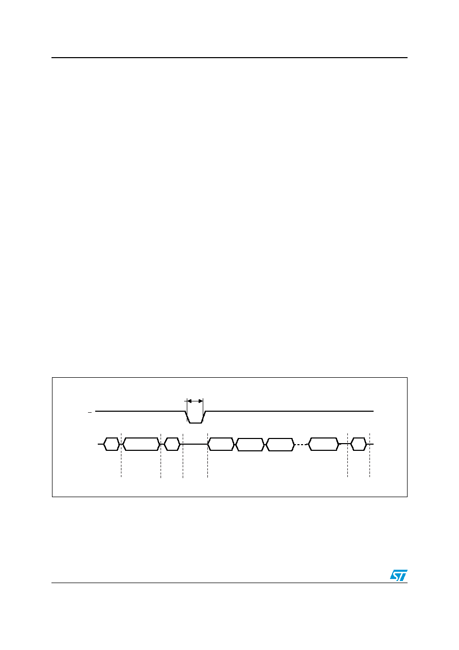
6.9
Read Electronic Signature
The device contains a Manufacturer Code and Device Code. To read these codes three steps
are required:
1.
one Bus Write cycle to issue the Read Electronic Signature command (90h)
2.
one Bus Write cycle to input the address (00h)
3.
four Bus Read Cycles to sequentially output the data (as shown in
Table 14: Electronic
Signature
).
Table 14.
Electronic Signature
Part Number
Byte/Word 1
Byte/Word 2
Byte/Word 3
Byte/Word 4
Manufacturer
Code
Device code
NAND01GR3B
20h
A1h
Reserved
80h
Page Size
Spare Area size
Sequential Access
Time
Block Size
Organization
(see
Table 15
)
NAND01GW3B
F1h
NAND01GR4B
0020h
B1h
NAND01GW4B
C1h
NAND02GR3B
20h
AAh
NAND02GW3B
DAh
NAND02GR4B
0020h
BAh
NAND02GW4B
CAh
Table 15.
Electronic Signature Byte/Word 4
I/O
Definition
Value
Description
I/O1-I/O0
Page Size
(Without Spare Area)
0 0
0 1
1 0
1 1
1K
2K
Reserved
Reserved
I/O2
Spare Area Size
(Byte / 512 Byte)
0
1
8
16
I/O3
Sequential Access Time
0
1
Standard (50 ns)
Fast (30 ns)
I/O5-I/O4
Block Size
(Without Spare Area)
0 0
0 1
1 0
1 1
64K
128K
256K
Reserved
I/O6
Organization
0
1
X8
X16
I/O7
Not Used
Reserved

Data protection
NAND01G-B, NAND02G-B
36/64
7 Data
protection
The device has both hardware and software features to protect against program and erase
operations.
It features a Write Protect, WP, pin, which can be used to protect the device against program
and erase operations. It is recommended to keep WP at V
IL
during power-up and power-
down.
In addition, to protect the memory from any involuntary program/erase operations during
power-transitions, the device has an internal voltage detector which disables all functions
whenever V
DD
is below V
LKO
(see
Table 22
and
Table 23
).
The device features a Block Lock mode, which is enabled by setting the Power-Up Read
Enable, Lock/Unlock Enable, PRL, signal to High.
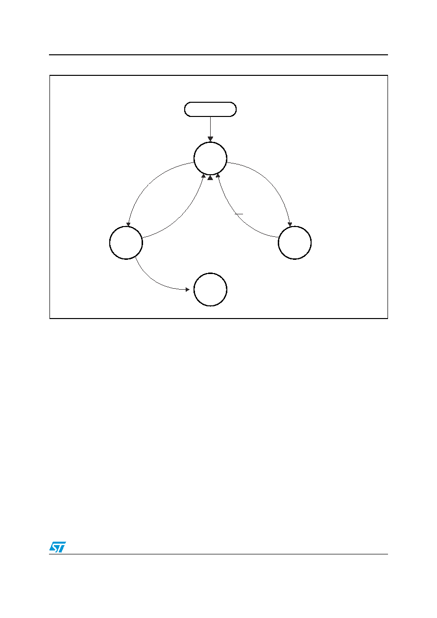
The Block Lock mode has two levels of software protection.
Blocks Lock/Unlock
Blocks Lock-down
Refer to
Figure 18
for an overview of the protection mechanism.
7.1 Blocks
Lock
All the blocks are locked simultaneously by issuing a Blocks Lock command (see
Table 10:
Commands
).
All blocks are locked after power-up and when the Write Protect signal is Low.
Once all the blocks are locked, one sequence of consecutive blocks can be unlocked by
using the Blocks Unlock command.
Refer to
Figure 23: Command Latch AC Waveforms
for details on how to issue the
command.
7.2 Blocks
Unlock
A sequence of consecutive locked blocks can be unlocked, to allow program or erase
operations, by issuing an Blocks Unlock command (see
Table 10: Commands
).
The Blocks Unlock command consists of four steps:
1.
One bus cycle to setup the command
2.
two or three bus cycles to give the Start Block Address (refer to
Table 8
,
Table 9
and
Figure 16
)
3.
one bus cycle to confirm the command
4.
two or three bus cycles to give the End Block Address (refer to
Table 8
,
Table 9
and
Figure 16
).
The Start Block Address must be nearer the logical LSB (Least Significant Bit) than End
Block Address.
NAND01G-B, NAND02G-B
Data protection
37/64
If the Start Block Address is the same as the End Block Address, only one block is unlocked.
Only one consecutive area of blocks can be unlocked at any one time. It is not possible to
unlock multiple areas.
Figure 16.
Blocks Unlock Operation
1.
Three address cycles are required for 2 Gb devices. 1Gb devices only require two address cycles.
7.3 Blocks
Lock-Down
The Lock-Down feature provides an additional level of protection. A Locked-down block
cannot be unlocked by a software command. Locked-Down blocks can only be unlocked by
setting the Write Protect signal to Low for a minimum of 100ns.
Only locked blocks can be locked-down. The command has no affect on unlocked blocks.
Refer to
Figure 23: Command Latch AC Waveforms
for details on how to issue the
command.
7.4 Block
Lock
Status
In Block Lock mode (PRL High) the Block Lock Status of each block can be checked by
issuing a Read Block Lock Status command (see
Table 10: Commands
).
The command consists of:
one bus cycle to give the command code
three bus cycles to give the block address
After this, a read cycle will then output the Block Lock Status on the I/O pins on the falling
edge of Chip Enable or Read Enable, whichever occurs last. Chip Enable or Read Enable
do not need to be toggled to update the status.
The Read Block Lock Status command will not be accepted while the device is busy (RB
Low).
The device will remain in Read Block Lock Status mode until another command is issued.
I/O
WP
Start Block Address, 3 cycles
ai08670
23h
Blocks Unlock
Command
Add1
Add2
Add3
24h
Add1
Add2
Add3
End Block Address, 3 cycles

Data protection
NAND01G-B, NAND02G-B
38/64
Figure 17.
Read Block Lock Status Operation
1.
Three address cycles are required for 2 Gb devices. 1Gb devices only require two address cycles.
1.
X = Don't Care.
I/O
R
Block Address, 3 cycles
ai08669
7Ah
Read Block Lock
Status Command
Add1
Add2
Add3
Dout
Block Lock Status
tWHRL
W
Table 16.
Block Lock Status
Status
I/O7-I/O3
I/O2
I/O1
I/O0
Locked
X
0
1
0
Unlocked
X
1
1
0
Locked-Down
X
0
0
1
Unlocked in
Locked-Down
Area
X
1
0
1
NAND01G-B, NAND02G-B
Data protection
39/64
Figure 18.
Block Protection State Diagram
1.
PRL must be High for the software commands to be accepted.
AI08663c
Locked
Locked-Down
Unlocked in
Locked Area
Power-Up
Block Unlock
Command
Blocks Lock-Down
Command
WP VIL >100ns
Blocks Lock
Command
WP VIL >100ns
(start + end block address)
Unlocked in
Locked-Down
Area
Blocks Lock-Down
Command
WP VIL >100ns

Software algorithms
NAND01G-B, NAND02G-B
40/64
8 Software
algorithms
This section gives information on the software algorithms that ST recommends to implement
to manage the Bad Blocks and extend the lifetime of the NAND device.
NAND Flash memories are programmed and erased by Fowler-Nordheim tunneling using a
high voltage. Exposing the device to a high voltage for extended periods can cause the
oxide layer to be damaged. For this reason, the number of program and erase cycles is
limited (see
Table 18
for value) and it is recommended to implement Garbage Collection, a
Wear-Leveling Algorithm and an Error Correction Code, to extend the number of program
and erase cycles and increase the data retention.
To help integrate a NAND memory into an application ST Microelectronics can provide a File
System OS Native reference software, which supports the basic commands of file
management.
Contact the nearest ST Microelectronics sales office for more details.
8.1 Bad
Block
Management
Devices with Bad Blocks have the same quality level and the same AC and DC
characteristics as devices where all the blocks are valid. A Bad Block does not affect the
performance of valid blocks because it is isolated from the bit line and common source line
by a select transistor.
The devices are supplied with all the locations inside valid blocks erased (FFh). The Bad
Block Information is written prior to shipping. Any block, where the 1st and 6th Bytes, or 1st
Word,
in the spare area of the 1st page, does not contain FFh, is a Bad Block.
The Bad Block Information must be read before any erase is attempted as the Bad Block
Information may be erased. For the system to be able to recognize the Bad Blocks based on
the original information it is recommended to create a Bad Block table following the
flowchart shown in
Figure 19
8.2 Block
Replacement
Over the lifetime of the device additional Bad Blocks may develop. In this case the block has
to be replaced by copying the data to a valid block. These additional Bad Blocks can be
identified as attempts to program or erase them will give errors in the Status Register.
As the failure of a page program operation does not affect the data in other pages in the
same block, the block can be replaced by re-programming the current data and copying the
rest of the replaced block to an available valid block. The Copy Back Program command can
be used to copy the data to a valid block.
See the
Section 6.4: Copy Back Program
for more details.
Refer to
Table 17
for the recommended procedure to follow if an error occurs during an
operation.
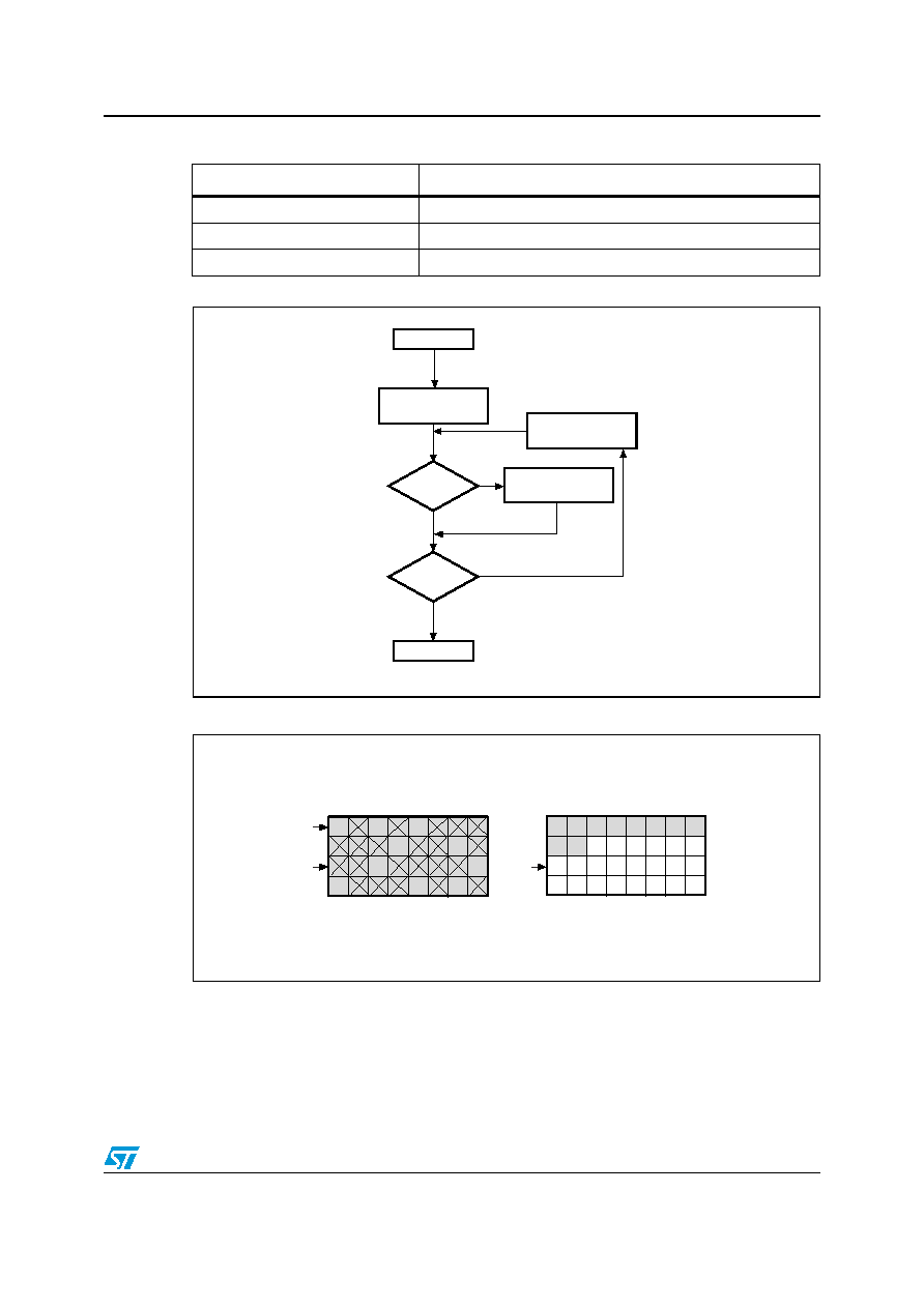
NAND01G-B, NAND02G-B
Software algorithms
41/64
Figure 19.
Bad Block Management Flowchart
Figure 20.
Garbage Collection
Table 17.
Block Failure
Operation
Recommended Procedure
Erase
Block Replacement
Program
Block Replacement or ECC
Read
ECC
AI07588C
START
END
NO
YES
YES
NO
Block Address =
Block 0
Data
= FFh?
Last
block?
Increment
Block Address
Update
Bad Block table
Valid
Page
Invalid
Page
Free
Page
(Erased)
Old Area
AI07599B
New Area (After GC)

Software algorithms
NAND01G-B, NAND02G-B
42/64
8.3 Garbage
Collection
When a data page needs to be modified, it is faster to write to the first available page, and
the previous page is marked as invalid. After several updates it is necessary to remove
invalid pages to free some memory space.
To free this memory space and allow further program operations it is recommended to
implement a Garbage Collection algorithm. In a Garbage Collection software the valid
pages are copied into a free area and the block containing the invalid pages is erased (see
Figure 20
).
8.4 Wear-leveling
algorithm
For write-intensive applications, it is recommended to implement a Wear-leveling Algorithm
to monitor and spread the number of write cycles per block.
In memories that do not use a Wear-Leveling Algorithm not all blocks get used at the same
rate. Blocks with long-lived data do not endure as many write cycles as the blocks with
frequently-changed data.
The Wear-leveling Algorithm ensures that equal use is made of all the available write cycles
for each block. There are two wear-leveling levels:
First Level Wear-leveling, new data is programmed to the free blocks that have had the
fewest write cycles
Second Level Wear-leveling, long-lived data is copied to another block so that the
original block can be used for more frequently-changed data.
The Second Level Wear-leveling is triggered when the difference between the maximum
and the minimum number of write cycles per block reaches a specific threshold.
8.5
Error Correction Code
An Error Correction Code (ECC) can be implemented in the NAND Flash memories to
identify and correct errors in the data.
For every 2048 bits in the device it is recommended to implement 22 bits of ECC (16 bits for
line parity plus 6 bits for column parity).
An ECC model is available in VHDL or Verilog. Contact the nearest ST Microelectronics
sales office for more details.
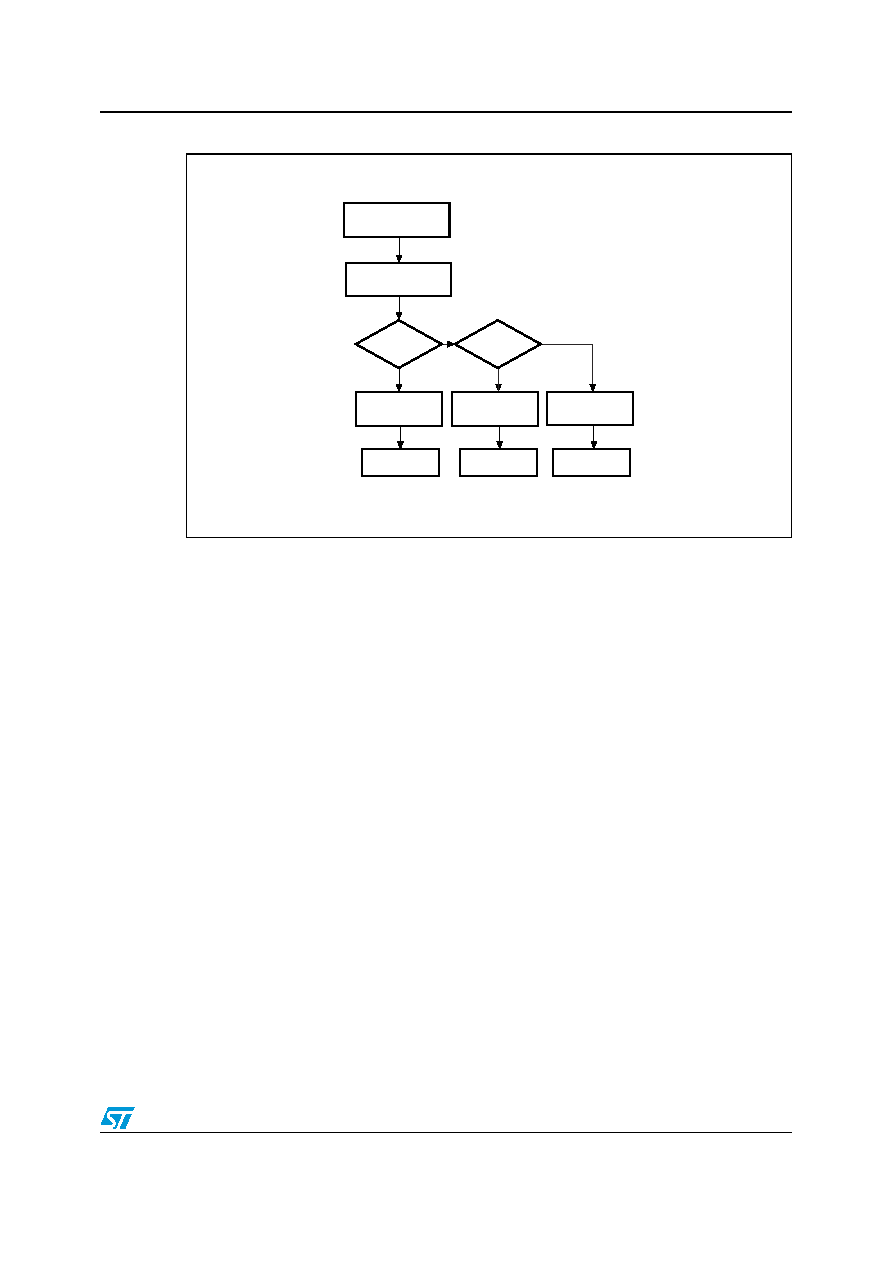
NAND01G-B, NAND02G-B
Software algorithms
43/64
Figure 21.
Error Detection
8.6
Hardware Simulation models
8.6.1
Behavioral simulation models
Denali Software Corporation models are platform independent functional models designed
to assist customers in performing entire system simulations (typical VHDL/Verilog). These
models describe the logic behavior and timings of NAND Flash devices, and so allow
software to be developed before hardware.
8.6.2 IBIS
simulations
models
IBIS (I/O Buffer Information Specification) models describe the behavior of the I/O buffers
and electrical characteristics of Flash devices.
These models provide information such as AC characteristics, rise/fall times and package
mechanical data, all of which are measured or simulated at voltage and temperature ranges
wider than those allowed by target specifications.
IBIS models are used to simulate PCB connections and can be used to resolve compatibility
issues when upgrading devices. They can be imported into SPICETOOLS.
New ECC generated
during read
XOR previous ECC
with new ECC
All results
= zero?
22 bit data = 0
YES
11 bit data = 1
NO
1 bit data = 1
Correctable
Error
ECC Error
No Error
ai08332
>1 bit
= zero?
YES
NO

Program and Erase Times and Endurance cycles
NAND01G-B, NAND02G-B
44/64
9
Program and Erase Times and Endurance cycles
The Program and Erase times and the number of Program/ Erase cycles per block are
shown in
Table 18
.
Table 18.
Program, Erase Times and Program Erase Endurance Cycles
Parameters
NAND Flash
Unit
Min
Typ
Max
Page Program Time
300
700
µs
Block Erase Time
2
3
ms
Program/Erase Cycles (per block)
100,000
cycles
Data Retention
10
years

NAND01G-B, NAND02G-B
Maximum rating
45/64
10 Maximum
rating
Stressing the device above the ratings listed in
Table 19: Absolute Maximum Ratings
, may
cause permanent damage to the device. These are stress ratings only and operation of the
device at these or any other conditions above those indicated in the Operating sections of
this specification is not implied. Exposure to Absolute Maximum Rating conditions for
extended periods may affect device reliability. Refer also to the STMicroelectronics SURE
Program and other relevant quality documents.
Table 19.
Absolute Maximum Ratings
Symbol
Parameter
Value
Unit
Min
Max
T
BIAS
Temperature Under Bias
≠ 50
125
∞C
T
STG
Storage Temperature
≠ 65
150
∞C
V
IO
(1)
1.
Minimum Voltage may undershoot to ≠2V for less than 20ns during transitions on input and I/O pins.
Maximum voltage may overshoot to V
DD
+ 2V for less than 20ns during transitions on I/O pins.
Input or Output Voltage
1.8V devices
≠ 0.6
2.7
V
3 V devices
≠ 0.6
4.6
V
V
DD
Supply Voltage
1.8V devices
≠ 0.6
2.7
V
3 V devices
≠ 0.6
4.6
V
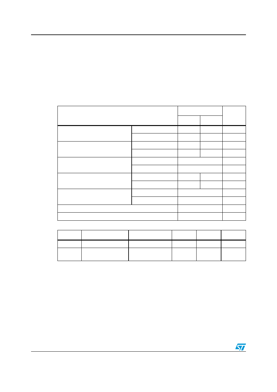
DC And AC parameters
NAND01G-B, NAND02G-B
46/64
11
DC And AC parameters
This section summarizes the operating and measurement conditions, and the DC and AC
characteristics of the device. The parameters in the DC and AC characteristics Tables that
follow, are derived from tests performed under the Measurement Conditions summarized in
Table 20: Operating and AC Measurement Conditions
. Designers should check that the
operating conditions in their circuit match the measurement conditions when relying on the
quoted parameters.
Table 20.
Operating and AC Measurement Conditions
Parameter
NAND Flash
Units
Min
Max
Supply Voltage (V
DD
)
1.8V devices
1.7
1.95
V
3V devices
2.7
3.6
V
Ambient Temperature (T
A
)
Grade 1
0
70
∞C
Grade 6
≠40
85
∞C
Load Capacitance (C
L
)
(1 TTL GATE and C
L
)
1.8V devices
30
pF
3V devices (2.7 - 3.6V)
50
pF
Input Pulses Voltages
1.8V devices
0
V
DD
V
3V devices
0.4
2.4
V
Input and Output Timing Ref. Voltages
1.8V devices
0.9
V
3V devices
1.5
V
Output Circuit Resistor R
ref
8.35
k
Input Rise and Fall Times
5
ns
Table 21.
Capacitance
(1)
1.
T
A
= 25∞C, f = 1 MHz. C
IN
and C
I/O
are not 100% tested
Symbol
Parameter
Test Condition
Typ
Max
Unit
C
IN
Input Capacitance
V
IN
= 0V
10
pF
C
I/O
Input/Output
Capacitance
(2)
2.
Input/output capacitances double in stacked devices
V
IL
= 0V
10
pF

NAND01G-B, NAND02G-B
DC And AC parameters
47/64
Figure 22.
Equivalent Testing Circuit for AC Characteristics Measurement
Table 22.
DC Characteristics, 1.8V Devices
Symbol
Parameter
Test Conditions
Min
Typ
Max
Unit
I
DD1
Operating
Current
Sequential
Read
t
RLRL
minimum
E=V
IL,
I
OUT
= 0 mA
-
8
15
mA
I
DD2
Program
-
-
8
15
mA
I
DD3
Erase
-
-
8
15
mA
I
DD5
Standby Current (CMOS)
(1)
E=V
DD
-0.2,
WP=0/V
DD
-
10
50
µA
I
LI
Input Leakage Current
(1)
V
IN
= 0 to V
DD
max
-
-
±10
µA
I
LO
Output Leakage Current
(1)
V
OUT
= 0 to V
DD
max
-
-
±10
µA
V
IH
Input High Voltage
-
V
DD
-0.4
-
V
DD
+0.3
V
V
IL
Input Low Voltage
-
-0.3
-
0.4
V
V
OH
Output High Voltage Level
I
OH
= -100µA
V
DD
-0.1
-
-
V
V
OL
Output Low Voltage Level
I
OL
= 100µA
-
-
0.1
V
I
OL
(RB)
Output Low Current (RB)
V
OL
= 0.1V
3
4
mA
V
LKO
V
DD
Supply Voltage (Erase and
Program lockout)
-
-
-
1.1
V
1.
Leakage current and standby current double in stacked devices
Ai11085
NAND Flash
CL
2Rref
VDD
2Rref
GND
GND

DC And AC parameters
NAND01G-B, NAND02G-B
48/64
Table 23.
DC Characteristics, 3V Devices
Symbol
Parameter
Test Conditions
Min
Typ
Max
Unit
I
DD1
Operating
Current
Sequential
Read
t
RLRL
minimum
E=V
IL,
I
OUT
= 0 mA
-
15
30
mA
I
DD2
Program
-
-
15
30
mA
I
DD3
Erase
-
-
15
30
mA
I
DD4
Standby current (TTL)
(1)
E=V
IH
, WP=0/V
DD
1
mA
I
DD5
Standby Current (CMOS)
(1)
E=V
DD
-0.2,
WP=0/V
DD
-
10
50
µA
I
LI
Input Leakage Current
(1)
V
IN
= 0 to V
DD
max
-
-
±10
µA
I
LO
Output Leakage Current
(1)
V
OUT
= 0 to V
DD
max
-
-
±10
µA
V
IH
Input High Voltage
-
0.8V
DD
-
V
DD
+0.3
V
V
IL
Input Low Voltage
-
-0.3
-
0.2V
DD
V
V
OH
Output High Voltage Level
I
OH
= -400µA
2.4
-
-
V
V
OL
Output Low Voltage Level
I
OL
= 2.1mA
-
-
0.4
V
I
OL
(RB)
Output Low Current (RB)
V
OL
= 0.4V
8
10
mA
V
LKO
V
DD
Supply Voltage (Erase and
Program lockout)
-
-
-
1.7
V
1.
Leakage current and standby current double in stacked devices

NAND01G-B, NAND02G-B
DC And AC parameters
49/64
Table 24.
AC Characteristics for Command, Address, Data Input
Symbol
Alt.
Symbol
Parameter
1.8V
Devices
3V
Devices
Unit
t
ALLWL
t
ALS
Address Latch Low to Write Enable Low
AL Setup time
Min
0
0
ns
t
ALHWL
Address Latch High to Write Enable Low
t
CLHWL
t
CLS
Command Latch High to Write Enable
Low
CL Setup time
Min
0
0
ns
t
CLLWL
Command Latch Low to Write Enable Low
t
DVWH
t
DS
Data Valid to Write Enable High
Data Setup time
Min
20
20
ns
t
ELWL
t
CS
Chip Enable Low to Write Enable Low
E Setup time
Min
0
0
ns
t
WHALH
t
ALH
Write Enable High to Address Latch High
AL Hold time
Min
10
10
ns
t
WHCLH
t
CLH
Write Enable High to Command Latch
High
CL hold time
Min
10
10
ns
t
WHCLL
Write Enable High to Command Latch
Low
t
WHDX
t
DH
Write Enable High to Data Transition
Data Hold time
Min
10
10
ns
t
WHEH
t
CH
Write Enable High to Chip Enable High
E Hold time
Min
10
10
ns
t
WHWL
t
WH
Write Enable High to Write Enable Low
W High Hold
time
Min
20
20
ns
t
WLWH
(1)
t
WP
Write Enable Low to Write Enable High
W Pulse Width
Min
25
25
ns
t
WLWL
t
WC
Write Enable Low to Write Enable Low
Write Cycle time
Min
60
50
ns
1.
If t
ELWL
is less than 10ns, t
WLWH
must be minimum 35ns, otherwise, t
WLWH
may be minimum 25ns.
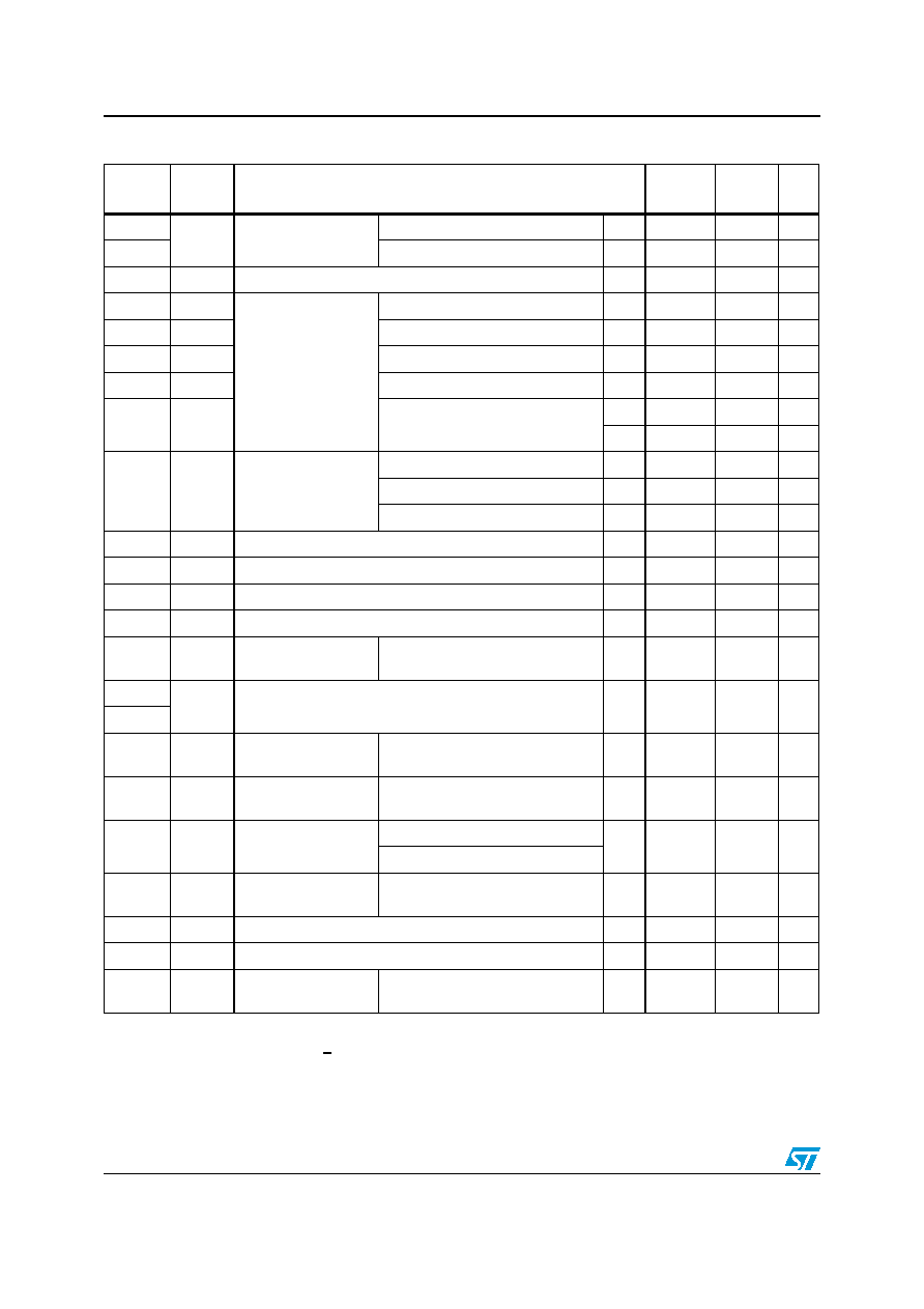
DC And AC parameters
NAND01G-B, NAND02G-B
50/64
Table 25.
AC Characteristics for Operations
(1)(2)
Symbol
Alt.
Symbol
Parameter
1.8V
Devices
3V
Devices
Unit
t
ALLRL1
t
AR
Address Latch Low to
Read Enable Low
Read Electronic Signature
Min
10
10
ns
t
ALLRL2
Read cycle
Min
10
10
ns
t
BHRL
t
RR
Ready/Busy High to Read Enable Low
Min
20
20
ns
t
BLBH1
Ready/Busy Low to
Ready/Busy High
Read Busy time
Max
25
25
µs
t
BLBH2
t
PROG
Program Busy time
Max
700
700
µs
t
BLBH3
t
BERS
Erase Busy time
Max
3
3
ms
t
BLBH4
Reset Busy time, during ready
Max
5
5
µs
t
BLBH5
t
CBSY
Cache Busy time
Typ
3
3
µs
Max
700
700
µs
t
WHBH1
t
RST
Write Enable High to
Ready/Busy High
Reset Busy time, during read
Max
5
5
µs
Reset Busy time, during program
Max
10
10
µs
Reset Busy time, during erase
Max
500
500
µs
t
CLLRL
t
CLR
Command Latch Low to Read Enable Low
Min
10
10
ns
t
DZRL
t
IR
Data Hi-Z to Read Enable Low
Min
0
0
ns
t
EHQZ
t
CHZ
Chip Enable High to Output Hi-Z
Max
20
20
ns
t
ELQV
t
CEA
Chip Enable Low to Output Valid
Max
45
45
ns
t
RHRL
t
REH
Read Enable High to
Read Enable Low
Read Enable High Hold time
Min
20
20
ns
T
EHQX
T
OH
Chip Enable high or Read Enable high to Output Hold
Min
15
15
ns
T
RHQX
t
RLRH
t
RP
Read Enable Low to
Read Enable High
Read Enable Pulse Width
Min
25
25
ns
t
RLRL
t
RC
Read Enable Low to
Read Enable Low
Read Cycle time
Min
60
50
ns
t
RLQV
t
REA
Read Enable Low to
Output Valid
Read Enable Access time
Max
35
35
ns
Read ES Access time
(3)
t
WHBH
t
R
Write Enable High to
Ready/Busy High
Read Busy time
Max
25
25
µs
t
WHBL
t
WB
Write Enable High to Ready/Busy Low
Max
100
100
ns
t
WHRL
t
WHR
Write Enable High to Read Enable Low
Min
60
60
ns
t
WLWL
t
WC
Write Enable Low to
Write Enable Low
Write Cycle time
Min
60
50
ns
1.
The time to Ready depends on the value of the pull-up resistor tied to the Ready/Busy pin. See
Figure 33
,
Figure 34
and
Figure 35
.
2.
To break the sequential read cycle, E must be held High for longer than t
EHEL
.
3.
ES = Electronic Signature.
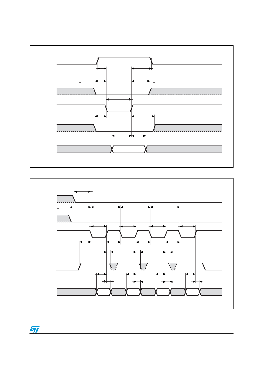
NAND01G-B, NAND02G-B
DC And AC parameters
51/64
Figure 23.
Command Latch AC Waveforms
Figure 24.
Address Latch AC Waveforms
1.
A fifth address cycle is required for 2Gb devices.
ai08028
CL
E
W
AL
I/O
tCLHWL
tELWL
tWHCLL
tWHEH
tWLWH
tALLWL
tWHALH
Command
tDVWH
tWHDX
(CL Setup time)
(CL Hold time)
(Data Setup time)
(Data Hold time)
(ALSetup time)
(AL Hold time)
(E Setup time)
(E Hold time)
ai08029
CL
E
W
AL
I/O
tWLWH
tELWL
tWLWL
tCLLWL
tWHWL
tALHWL
tDVWH
tWLWL
tWLWL
tWLWH
tWLWH
tWLWH
tWHWL
tWHWL
tWHDX
tWHALL
tDVWH
tWHDX
tDVWH
tWHDX
tDVWH
tWHDX
tWHALL
Adrress
cycle 1
tWHALL
(AL Setup time)
(AL Hold time)
Adrress
cycle 4
Adrress
cycle 3
Adrress
cycle 2
(CL Setup time)
(Data Setup time)
(Data Hold time)
(E Setup time)
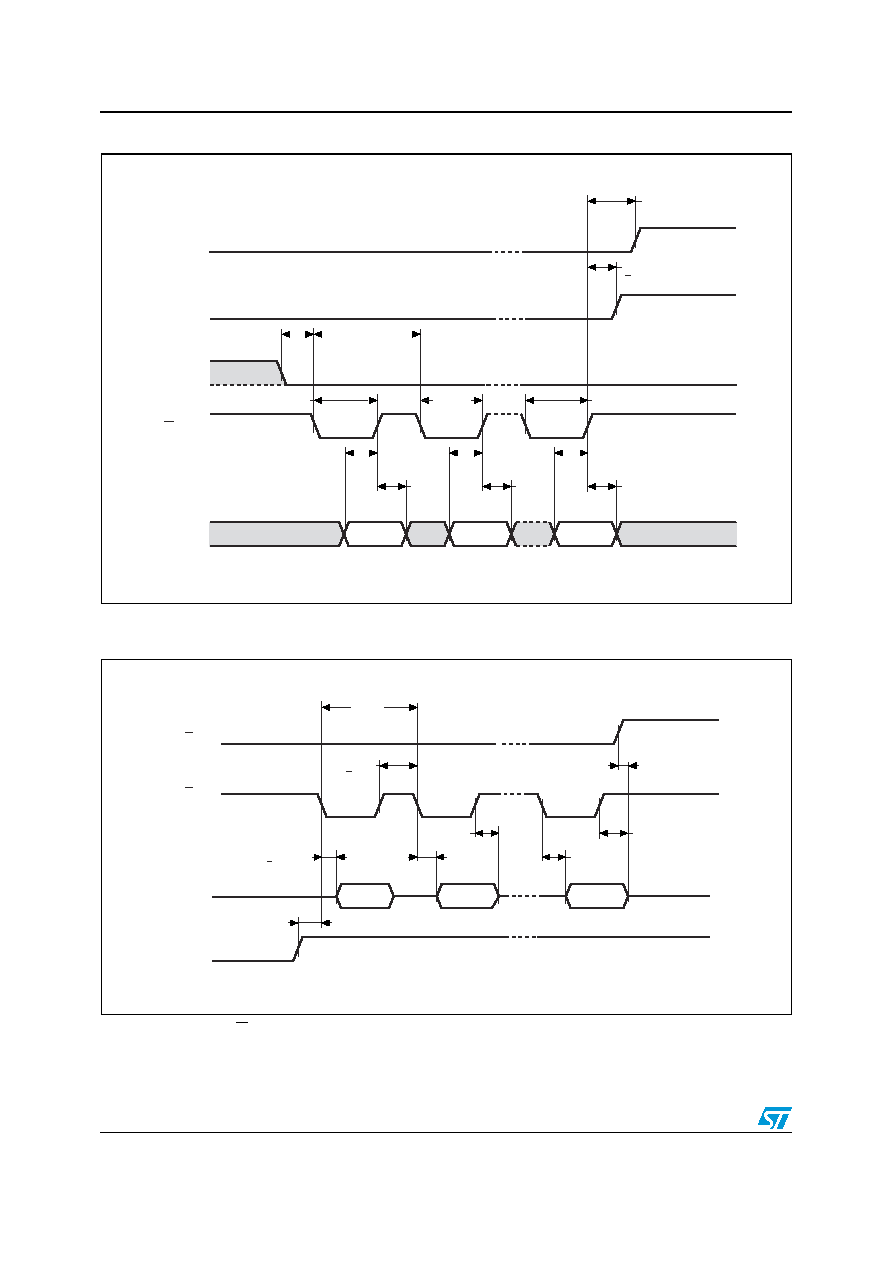
DC And AC parameters
NAND01G-B, NAND02G-B
52/64
Figure 25.
Data Input Latch AC Waveforms
1.
Data In Last is 2112 in x8 devices and 1056 in x16 devices.
Figure 26.
Sequential Data Output after Read AC Waveforms
1.
CL = Low, AL = Low, W = High.
tWHCLH
CL
E
AL
W
I/O
tALLWL
tWLWL
tWLWH
tWHEH
tWLWH
tWLWH
Data In 0
Data In 1
Data In
Last
tDVWH
tWHDX
tDVWH
tWHDX
tDVWH
tWHDX
ai08030
(Data Setup time)
(Data Hold time)
(ALSetup time)
(CL Hold time)
(E Hold time)
E
ai08031
R
I/O
RB
tRLRL
tRLQV
tRHRL
tRLQV
Data Out
Data Out
Data Out
tRHQZ
tBHRL
tRLQV
tRHQZ
tEHQZ
(Read Cycle time)
(R Accesstime)
(R High Holdtime)

NAND01G-B, NAND02G-B
DC And AC parameters
53/64
Figure 27.
Read Status Register AC Waveform
Figure 28.
Read Electronic Signature AC Waveform
1.
Refer to
Table 14
for the values of the Manufacturer and Device Codes, and to
Table 15
for the information contained in
Byte4.
tELWL
tDVWH
Status Register
Output
70h/ 72h/
73h/ 74h/ 75h
CL
E
W
R
I/O
tCLHWL
tWHDX
tWLWH
tWHCLL
tCLLRL
tDZRL
tRLQV
tEHQZ
tRHQZ
tWHRL
tELQV
tWHEH
ai08666
(Data Setup time)
(Data Hold time)
90h
00h
Man.
code
Device
code
CL
E
W
AL
R
I/O
tRLQV
Read Electronic
Signature
Command
1st Cycle
Address
ai08667
(Read ES Access time)
tALLRL1
00h
Byte4
Byte3
Byte1
Byte2
see Note.1
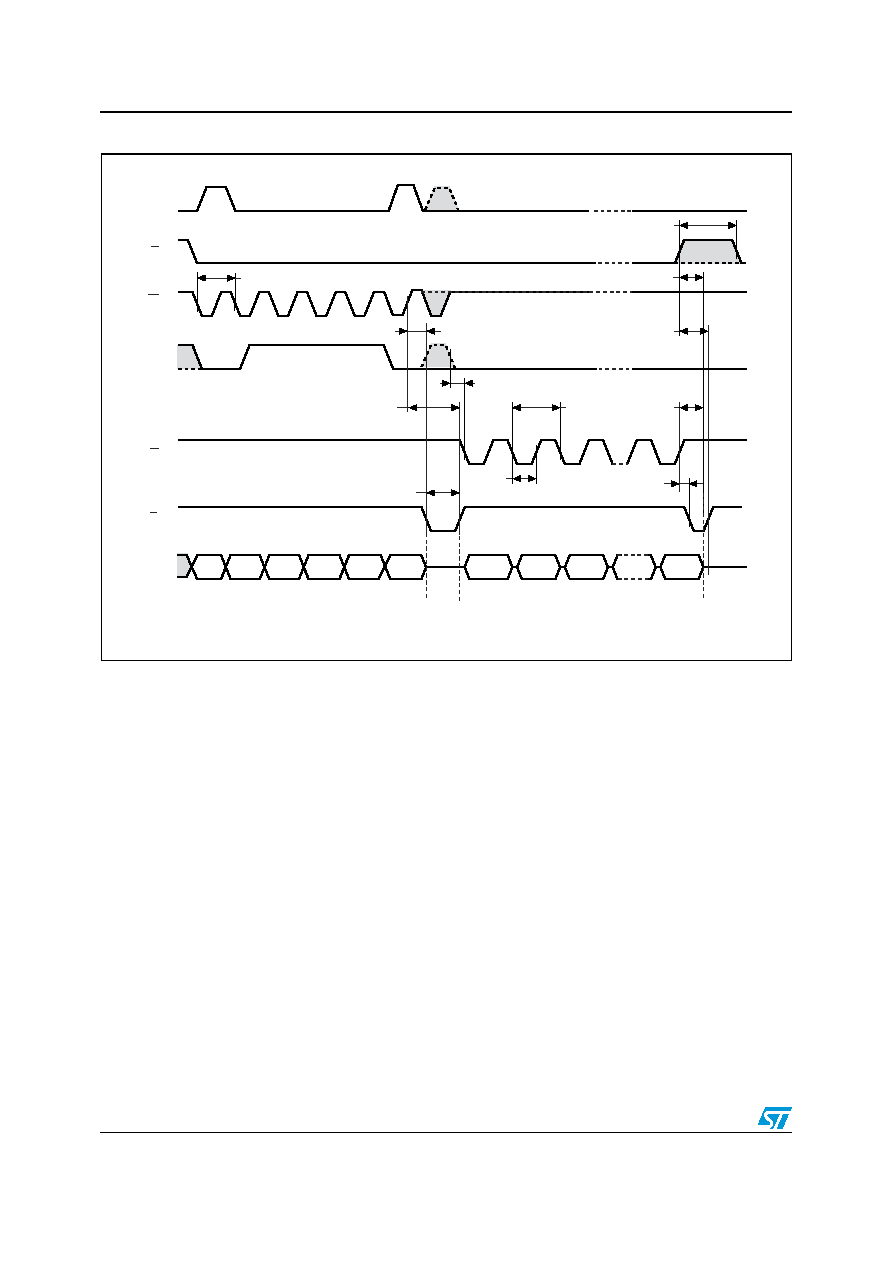
DC And AC parameters
NAND01G-B, NAND02G-B
54/64
Figure 29.
Page Read Operation AC Waveform
1.
A fifth address cycle is required for 2Gb devices.
tEHEL
CL
E
W
AL
R
I/O
RB
tWLWL
tWHBL
tALLRL2
00h
Data
N
Data
N+1
Data
N+2
Data
Last
tRHBL
tEHBH
tWHBH
tRLRL
tEHQZ
tRHQZ
ai08660
Busy
Command
Code
Address N Input
Data Output
from Address N to Last Byte or Word in Page
Add.N
cycle 1
Add.N
cycle 4
Add.N
cycle 3
Add.N
cycle 2
(Read Cycle time)
tRLRH
tBLBH1
30h

NAND01G-B, NAND02G-B
DC And AC parameters
55/64
Figure 30.
Page Program AC Waveform
1.
A fifth address cycle is required for 2Gb devices.
CL
E
W
AL
R
I/O
RB
SR0
ai08668
N
Last
10h
70h
80h
Page Program
Setup Code
Confirm
Code
Read Status Register
tWLWL
tWLWL
tWLWL
tWHBL
tBLBH2
Page
Program
Address Input
Data Input
Add.N
cycle 1
Add.N
cycle 4
Add.N
cycle 3
Add.N
cycle 2
(Write Cycle time)
(Program Busy time)
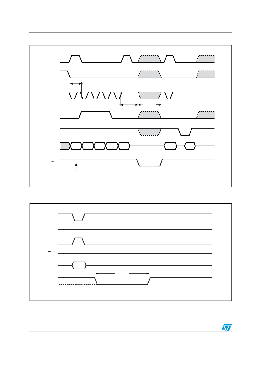
DC And AC parameters
NAND01G-B, NAND02G-B
56/64
Figure 31.
Block Erase AC Waveform
1.
Address cycle 3 is required for 2Gb devices only.
Figure 32.
Reset AC Waveform
D0h
60h
SR0
70h
ai08038b
tWHBL
tWLWL
tBLBH3
Block Erase
Setup Command
Block Erase
CL
E
W
AL
R
I/O
RB
Confirm
Code
Read Status Register
Block Address Input
(Erase Busy time)
(Write Cycle time)
Add.
cycle 1
Add.
cycle 3
Add.
cycle 2
W
R
I/O
RB
tBLBH4
AL
CL
FFh
ai08043
(Reset Busy time)
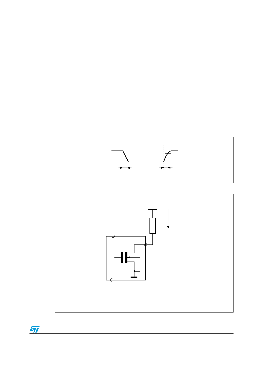
NAND01G-B, NAND02G-B
DC And AC parameters
57/64
11.1
Ready/Busy Signal electrical characteristics
Figure 34
,
Figure 33
and
Figure 35
show the electrical characteristics for the Ready/Busy
signal. The value required for the resistor R
P
can be calculated using the following equation:
So,
where I
L
is the sum of the input currents of all the devices tied to the Ready/Busy signal. R
P
max is determined by the maximum value of t
r
.
Figure 33.
Ready/Busy AC Waveform
Figure 34.
Ready/Busy Load Circuit
R
P
min
VDDmax VOLmax
≠
(
)
IOL
IL
+
-------------------------------------------------------------
=
R
P
min 1.8V
(
)
1.85V
3mA
IL
+
---------------------------
=
R
P
min 3V
(
)
3.2V
8mA
IL
+
---------------------------
=
AI07564B
busy
VOH
ready VDD
VOL
tf
tr
AI07563B
RP
VDD
VSS
RB
DEVICE
Open Drain Output
ibusy
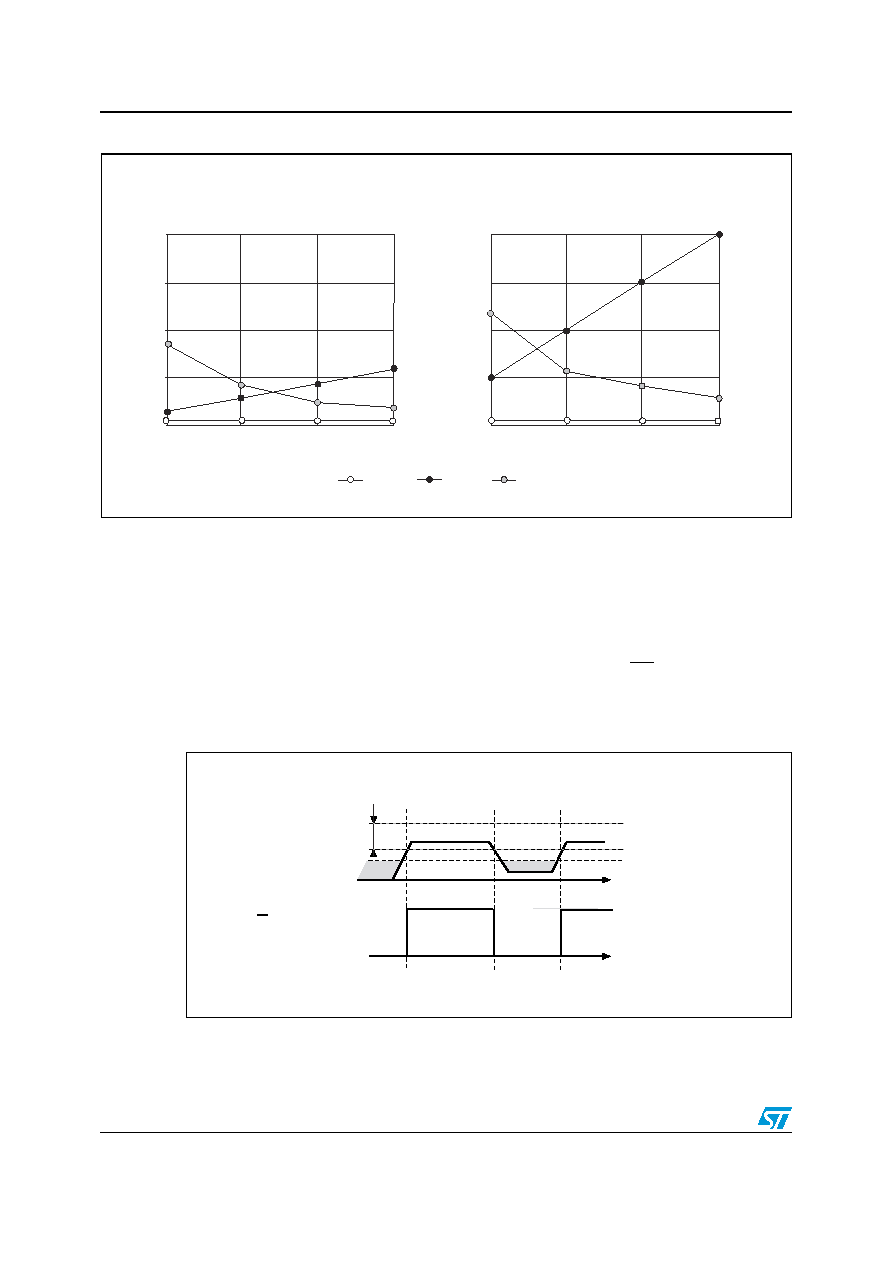
DC And AC parameters
NAND01G-B, NAND02G-B
58/64
Figure 35.
Resistor Value Versus Waveform Timings For Ready/Busy Signal
1.
T = 25∞C.
11.2 Data
Protection
The ST NAND device is designed to guarantee Data Protection during Power Transitions.
A V
DD
detection circuit disables all NAND operations, if V
DD
is below the V
LKO
threshold.
In the V
DD
range from V
LKO
to the lower limit of nominal range, the WP pin should be kept
low (V
IL
) to guarantee hardware protection during power transitions as shown in the below
figure.
Figure 36.
Data Protection
ai07565B
RP (K
)
1
2
3
4
100
300
200
t r
, t
f
(ns)
1
2
3
1.7
0.85
30
1.7
1.7
1.7
1.7
tr
tf
ibusy
0
400
4
RP (K
)
1
2
3
4
100
300
200
1
2
3
ibusy
(mA)
2.4
1.2
0.8
0.6
100
200
300
400
3.6
3.6
3.6
3.6
0
400
4
VDD = 1.8V, CL = 30pF
VDD = 3.3V, CL = 100pF
t r
, t
f
(ns)
ibusy
(mA)
60
90
120
0.57
0.43
Ai11086
VLKO
VDD
W
Nominal Range
Locked
Locked
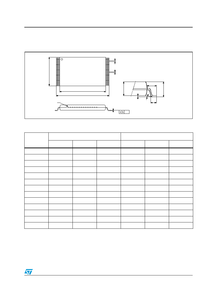
NAND01G-B, NAND02G-B
Package mechanical
59/64
12 Package
mechanical
Figure 37.
TSOP48 - 48 lead Plastic Thin Small Outline, 12 x 20 mm, Package Outline
1.
Drawing is not to scale.
TSOP-G
B
e
DIE
C
L
A1
E1
E
A
A2
1
24
48
25
D1
L1
CP
Table 26.
TSOP48 - 48 lead Plastic Thin Small Outline, 12 x 20 mm, Package Mechanical Data
Symbol
millimeters
inches
Typ
Min
Max
Typ
Min
Max
A
1.200
0.0472
A1
0.100
0.050
0.150
0.0039
0.0020
0.0059
A2
1.000
0.950
1.050
0.0394
0.0374
0.0413
B
0.220
0.170
0.270
0.0087
0.0067
0.0106
C
0.100
0.210
0.0039
0.0083
CP
0.080
0.0031
D1
12.000
11.900
12.100
0.4724
0.4685
0.4764
E
20.000
19.800
20.200
0.7874
0.7795
0.7953
E1
18.400
18.300
18.500
0.7244
0.7205
0.7283
e
0.500
≠
≠
0.0197
≠
L
0.600
0.500
0.700
0.0236
0.0197
0.0276
L1
0.800
0.0315
a
3∞
0∞
5∞
3∞
0∞
5∞
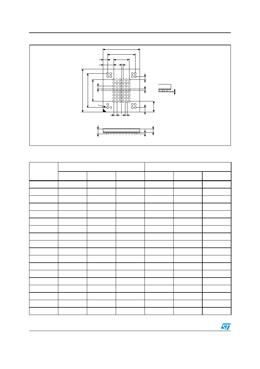
Package mechanical
NAND01G-B, NAND02G-B
60/64
Figure 38.
VFBGA63 9.5x12mm - 6x8 active ball array, 0.80mm pitch, Package Outline
1.
Drawing is not to scale
E
D
e
b
SD
SE
A2
A1
A
BGA-Z67
ddd
FD1
D2
E2
e
FE
FE1
e
E1
D1
FD
BALL "A1"
Table 27.
VFBGA63 9.5x12mm - 6x8 active ball array, 0.80mm pitch, Package Mechanical Data
Symbol
millimeters
inches
Typ
Min
Max
Typ
Min
Max
A
1.05
0.0413
A1
0.25
0.0098
A2
0.70
0.0276
b
0.45
0.40
0.50
0.0177
0.0157
0.0197
D
9.50
9.40
9.60
0.3740
0.3701
0.3780
D1
4.00
0.1575
D2
7.20
0.2835
ddd
0.10
0.0039
E
12.00
11.90
12.10
0.4724
0.4685
0.4764
E1
5.60
0.2205
E2
8.80
0.3465
e
0.80
≠
≠
0.0315
≠
≠
FD
2.75
0.1083
FD1
1.15
0.0453
FE
3.20
0.1260
FE1
1.60
0.0630
SD
0.40
0.0157
SE
0.40
0.0157
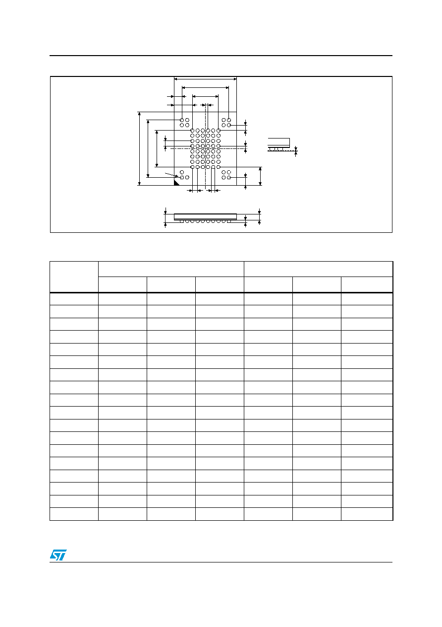
NAND01G-B, NAND02G-B
Package mechanical
61/64
Figure 39.
TFBGA63 9.5x12mm - 6x8 active ball array, 0.80mm pitch, Package Outline
1.
Drawing is not to scale
E
D
e
b
SD
SE
A2
A1
A
ddd
FD1
D2
E2
e
FE
FE1
e
E1
D1
FD
BALL "A1"
Table 28.
TFBGA63 9.5x12mm - 6x8 active ball array, 0.80mm pitch, Package Mechanical Data
Symbol
millimeters
inches
Typ
Min
Max
Typ
Min
Max
A
1.20
0.0472
A1
0.25
0.0098
A2
0.80
0.0315
b
0.45
0.40
0.50
0.0177
0.0157
0.0197
D
9.50
9.40
9.60
0.3740
0.3701
0.3780
D1
4.00
0.1575
D2
7.20
0.2835
ddd
0.10
0.0039
E
12.00
11.90
12.10
0.4724
0.4685
0.4764
E1
5.60
0.2205
E2
8.80
0.3465
e
0.80
≠
≠
0.0315
≠
≠
FD
2.75
0.1083
FD1
1.15
0.0453
FE
3.20
0.1260
FE1
1.60
0.0630
SD
0.40
0.0157
SE
0.40
0.0157

Part numbering
NAND01G-B, NAND02G-B
62/64
13 Part
numbering
Devices are shipped from the factory with the memory content bits, in valid blocks, erased to
'1'. For further information on any aspect of this device, please contact your nearest ST
Sales Office.
Table 29.
Ordering Information Scheme
Example:
NAND02GR3B
2
A
N
6
E
Device Type
NAND Flash Memory
Density
01G = 1Gb
02G = 2Gb
Operating Voltage
R = V
DD
= 1.7 to 1.95V
W = V
DD
= 2.7 to 3.6V
Bus Width
3 = x8
4 = x16
Family Identifier
B = 2112 Bytes/ 1056 Word Page
Device Options
2 = Chip Enable Don't Care Enabled
Product Version
A = First Version
B= Second Version
C= Third Version
Package
N = TSOP48 12 x 20mm (all devices)
ZA = VFBGA63 9.5 x 12 x 1mm, 0.8mm pitch (1Gb devices)
ZB = TFBGA63 9.5 x 12 x 1.2mm, 0.8mm pitch (2Gb Dual Die devices)
Temperature Range
1 = 0 to 70 ∞C
6 = ≠40 to 85 ∞C
Option
E = Lead Free Package, Standard Packing
F = Lead Free Package, Tape & Reel Packing

NAND01G-B, NAND02G-B
Revision history
63/64
14 Revision
history
Table 30.
Document Revision History
Date
Version
Revision Details
25-Feb-2005
1
First Issue
16-Aug-2005
2
Automatic Page 0 Read feature removed throughout document.
LFBGA63 package removed throughout document.
Section 11.2: Data Protection
and
Figure 22: Equivalent Testing
Circuit for AC Characteristics Measurement
added.
TFBGA63 and VFBGA63 packages updated. Note added to
Figure 3:
TSOP48 Connections, x8 devices
and
Table 3: TSOP48 Connections, x8
devices
regarding the USOP package.
Section 3.8: Write Enable (W)
,
Table 11
,
Table 12
,
Table 14
,
Section 7.4: Block Lock Status
,
Figure 18
,
Table 20
,
Table 22
,
Table 23
,
Table 25
and
Table 30
modified.
18-Oct-2005
3
512 device and USOP package removed throughout document.
Figure 3
, <Blue>Figure 5.,
Table 22
,
Table 23
and
Section 6.4: Copy
Back Program
modified.
13-Feb-2006
4.0
4 Gbit and 8 Git devices removed.
V
IH
minimum value and V
IL
maximum value updated in
Table 23: DC
Characteristics, 3V Devices
.

NAND01G-B, NAND02G-B
64/64
Please Read Carefully:
Information in this document is provided solely in connection with ST products. STMicroelectronics NV and its subsidiaries ("ST") reserve the
right to make changes, corrections, modifications or improvements, to this document, and the products and services described herein at any
time, without notice.
All ST products are sold pursuant to ST's terms and conditions of sale.
Purchasers are solely responsible for the choice, selection and use of the ST products and services described herein, and ST assumes no
liability whatsoever relating to the choice, selection or use of the ST products and services described herein.
No license, express or implied, by estoppel or otherwise, to any intellectual property rights is granted under this document. If any part of this
document refers to any third party products or services it shall not be deemed a license grant by ST for the use of such third party products
or services, or any intellectual property contained therein or considered as a warranty covering the use in any manner whatsoever of such
third party products or services or any intellectual property contained therein.
UNLESS OTHERWISE SET FORTH IN ST'S TERMS AND CONDITIONS OF SALE ST DISCLAIMS ANY EXPRESS OR IMPLIED
WARRANTY WITH RESPECT TO THE USE AND/OR SALE OF ST PRODUCTS INCLUDING WITHOUT LIMITATION IMPLIED
WARRANTIES OF MERCHANTABILITY, FITNESS FOR A PARTICULAR PURPOSE (AND THEIR EQUIVALENTS UNDER THE LAWS
OF ANY JURISDICTION), OR INFRINGEMENT OF ANY PATENT, COPYRIGHT OR OTHER INTELLECTUAL PROPERTY RIGHT.
UNLESS EXPRESSLY APPROVED IN WRITING BY AN AUTHORIZE REPRESENTATIVE OF ST, ST PRODUCTS ARE NOT DESIGNED,
AUTHORIZED OR WARRANTED FOR USE IN MILITARY, AIR CRAFT, SPACE, LIFE SAVING, OR LIFE SUSTAINING APPLICATIONS,
NOR IN PRODUCTS OR SYSTEMS, WHERE FAILURE OR MALFUNCTION MAY RESULT IN PERSONAL INJURY, DEATH, OR
SEVERE PROPERTY OR ENVIRONMENTAL DAMAGE.
Resale of ST products with provisions different from the statements and/or technical features set forth in this document shall immediately void
any warranty granted by ST for the ST product or service described herein and shall not create or extend in any manner whatsoever, any
liability of ST.
ST and the ST logo are trademarks or registered trademarks of ST in various countries.
Information in this document supersedes and replaces all information previously supplied.
The ST logo is a registered trademark of STMicroelectronics. All other names are the property of their respective owners.
© 2006 STMicroelectronics - All rights reserved
STMicroelectronics group of companies
Australia - Belgium - Brazil - Canada - China - Czech Republic - Finland - France - Germany - Hong Kong - India - Israel - Italy - Japan -
Malaysia - Malta - Morocco - Singapore - Spain - Sweden - Switzerland - United Kingdom - United States of America
www.st.com