Document Outline
- FEATURES SUMMARY
- SUMMARY DESCRIPTION
- MEMORY ARRAY ORGANIZATION
- SIGNAL DESCRIPTIONS
- BUS OPERATIONS
- COMMAND SET
- DEVICE OPERATIONS
- DATA PROTECTION
- SOFTWARE ALGORITHMS
- PROGRAM AND ERASE TIMES AND ENDURANCE CYCLES
- MAXIMUM RATING
- DC AND AC PARAMETERS
- PACKAGE MECHANICAL
- Figure 38. TSOP48 - 48 lead Plastic Thin Small Outline, 12 x 20 mm, Package Outline
- Table 26. TSOP48 - 48 lead Plastic Thin Small Outline, 12 x 20 mm, Package Mechanical Data
- Figure 39. USOP48 Ö lead Plastic Ultra Thin Small Outline,12x17 mm, Package Outline
- Table 27. USOP48 Ö lead Plastic Ultra Thin Small Outline, 12x17mm, Package Mechanical Data
- Figure 40. VFBGA63 9.5x12mm - 6x8 active ball array, 0.80mm pitch, Package Outline
- Table 28. VFBGA63 9.5x12mm - 6x8 active ball array, 0.80mm pitch, Package Mechanical Data
- Figure 41. TFBGA63 9.5x12mm - 6x8 active ball array, 0.80mm pitch, Package Outline
- Table 29. TFBGA63 9.5x12mm - 6x8 active ball array, 0.80mm pitch, Package Mechanical Data
- Figure 42. LFBGA63 9.5x12mm - 6x8 active ball array, 0.80mm pitch, Package Outline
- Table 30. LFBGA63 9.5x12mm - 6x8 active ball array, 0.80mm pitch, Package Mechanical Data
- PART NUMBERING
- REVISION HISTORY

1/59
PRELIMINARY DATA
February 2005
This is preliminary information on a new product now in development or undergoing evaluation. Details are subject to change without notice.
NAND512-B, NAND01G-B NAND02G-B
NAND04G-B NAND08G-B
512 Mbit, 1 Gbit, 2 Gbit, 4 Gbit, 8 Gbit
2112 Byte/1056 Word Page, 1.8V/3V, NAND Flash Memory
FEATURES SUMMARY
HIGH DENSITY NAND FLASH MEMORIES
≠
Up to 8 Gbit memory array
≠
Up to 64Mbit spare area
≠
Cost effective solutions for mass storage
applications
NAND INTERFACE
≠
x8 or x16 bus width
≠
Multiplexed Address/ Data
≠
Pinout compatibility for all densities
SUPPLY VOLTAGE
≠
1.8V device: V
DD
= 1.7 to 1.95V
≠
3.0V device: V
DD
= 2.7 to 3.6V
PAGE SIZE
≠
x8 device: (2048 + 64 spare) Bytes
≠
x16 device: (1024 + 32 spare) Words
BLOCK SIZE
≠
x8 device: (128K + 4K spare) Bytes
≠
x16 device: (64K + 2K spare) Words
PAGE READ / PROGRAM
≠
Random access: 25µs (max)
≠
Sequential access: 50ns (min)
≠
Page program time: 300µs (typ)
COPY BACK PROGRAM MODE
≠
Fast page copy without external buffering
CACHE PROGRAM AND CACHE READ
MODES
≠
Internal Cache Register to improve the
program and read throughputs
FAST BLOCK ERASE
≠
Block erase time: 2ms (typ)
STATUS REGISTER
ELECTRONIC SIGNATURE
CHIP ENABLE `DON'T CARE'
≠
for simple interface with microcontroller
AUTOMATIC PAGE 0 READ AT POWER-UP
≠
Boot from NAND support
SERIAL NUMBER OPTION
Figure 1. Packages
DATA PROTECTION
≠
Hardware and Software Block Locking
≠
Hardware Program/Erase locked during
Power transitions
DATA INTEGRITY
≠
100,000 Program/Erase cycles
≠
10 years Data Retention
RoHS COMPLIANCE
≠
Lead-Free Components are Compliant
with the RoHS Directive
DEVELOPMENT TOOLS
≠
Error Correction Code software and
hardware models
≠
Bad Blocks Management and Wear
Leveling algorithms
≠
PC Demo board with simulation software
≠
File System OS Native reference software
≠
Hardware simulation models
TSOP48 12 x 20mm
VFBGA63 9.5 x 12 x 1mm
TFBGA63 9.5 x 12 x 1.2mm
LFBGA63 9.5 x 12 x 1.4mm
FBGA
USOP48 12 x 17 x 0.65mm
NAND512-B, NAND01G-B, NAND02G-B, NAND04G-B, NAND08G-B
2/59
Table 1. Product List
Reference
Part Number
NAND512-B
NAND512R3B
NAND512W3B
NAND512R4B
NAND512W4B
NAND01G-B
NAND01GR3B
NAND01GW3B
NAND01GR4B
NAND01GW4B
NAND02G-B
NAND02GR3B
NAND02GW3B
NAND02GR4B
NAND02GW4B
NAND04G-B
NAND04GR3B
NAND04GW3B
NAND04GR4B
NAND04GW4B
NAND08G-B
NAND08GR3B
NAND08GW3B
NAND08GR4B
NAND08GW4B

3/59
NAND512-B, NAND01G-B, NAND02G-B, NAND04G-B, NAND08G-B
TABLE OF CONTENTS
FEATURES SUMMARY . . . . . . . . . . . . . . . . . . . . . . . . . . . . . . . . . . . . . . . . . . . . . . . . . . . . . . . . . . . . . 1
Figure 1. Packages . . . . . . . . . . . . . . . . . . . . . . . . . . . . . . . . . . . . . . . . . . . . . . . . . . . . . . . . . . . . . . 1
Table 1. Product List . . . . . . . . . . . . . . . . . . . . . . . . . . . . . . . . . . . . . . . . . . . . . . . . . . . . . . . . . . . . 2
SUMMARY DESCRIPTION. . . . . . . . . . . . . . . . . . . . . . . . . . . . . . . . . . . . . . . . . . . . . . . . . . . . . . . . . . . 7
Table 2. Product Description . . . . . . . . . . . . . . . . . . . . . . . . . . . . . . . . . . . . . . . . . . . . . . . . . . . . . . 8
Figure 2. Logic Block Diagram . . . . . . . . . . . . . . . . . . . . . . . . . . . . . . . . . . . . . . . . . . . . . . . . . . . . . 8
Figure 3. Logic Diagram . . . . . . . . . . . . . . . . . . . . . . . . . . . . . . . . . . . . . . . . . . . . . . . . . . . . . . . . . . 9
Table 3. Signal Names . . . . . . . . . . . . . . . . . . . . . . . . . . . . . . . . . . . . . . . . . . . . . . . . . . . . . . . . . . 9
Figure 4. TSOP48 and USOP48 Connections, x8 devices. . . . . . . . . . . . . . . . . . . . . . . . . . . . . . . 10
Figure 5. TSOP48 and USOP48 Connections, x16 devices. . . . . . . . . . . . . . . . . . . . . . . . . . . . . . 10
Figure 6. FBGA63 Connections, x8 devices (Top view through package) . . . . . . . . . . . . . . . . . . . 11
Figure 7. FBGA63 Connections, x16 devices (Top view through package) . . . . . . . . . . . . . . . . . . 12
MEMORY ARRAY ORGANIZATION . . . . . . . . . . . . . . . . . . . . . . . . . . . . . . . . . . . . . . . . . . . . . . . . . . 13
Bad Blocks . . . . . . . . . . . . . . . . . . . . . . . . . . . . . . . . . . . . . . . . . . . . . . . . . . . . . . . . . . . . . . . . . . . 13
Table 4. Valid Blocks . . . . . . . . . . . . . . . . . . . . . . . . . . . . . . . . . . . . . . . . . . . . . . . . . . . . . . . . . . . 13
Figure 8. Memory Array Organization. . . . . . . . . . . . . . . . . . . . . . . . . . . . . . . . . . . . . . . . . . . . . . . 13
SIGNAL DESCRIPTIONS . . . . . . . . . . . . . . . . . . . . . . . . . . . . . . . . . . . . . . . . . . . . . . . . . . . . . . . . . . . 14
Inputs/Outputs (I/O0-I/O7). . . . . . . . . . . . . . . . . . . . . . . . . . . . . . . . . . . . . . . . . . . . . . . . . . . . . . . . 14
Inputs/Outputs (I/O8-I/O15). . . . . . . . . . . . . . . . . . . . . . . . . . . . . . . . . . . . . . . . . . . . . . . . . . . . . . . 14
Address Latch Enable (AL) . . . . . . . . . . . . . . . . . . . . . . . . . . . . . . . . . . . . . . . . . . . . . . . . . . . . . . . 14
Command Latch Enable (CL) . . . . . . . . . . . . . . . . . . . . . . . . . . . . . . . . . . . . . . . . . . . . . . . . . . . . . 14
Chip Enable (E). . . . . . . . . . . . . . . . . . . . . . . . . . . . . . . . . . . . . . . . . . . . . . . . . . . . . . . . . . . . . . . . 14
Read Enable (R). . . . . . . . . . . . . . . . . . . . . . . . . . . . . . . . . . . . . . . . . . . . . . . . . . . . . . . . . . . . . . . . 14
Power-Up Read Enable, Lock/Unlock Enable (PRL). . . . . . . . . . . . . . . . . . . . . . . . . . . . . . . . . . . . 14
Write Enable (W). . . . . . . . . . . . . . . . . . . . . . . . . . . . . . . . . . . . . . . . . . . . . . . . . . . . . . . . . . . . . . . 14
Write Protect (WP). . . . . . . . . . . . . . . . . . . . . . . . . . . . . . . . . . . . . . . . . . . . . . . . . . . . . . . . . . . . . . 14
Ready/Busy (RB). . . . . . . . . . . . . . . . . . . . . . . . . . . . . . . . . . . . . . . . . . . . . . . . . . . . . . . . . . . . . . . 14
V
DD
Supply Voltage . . . . . . . . . . . . . . . . . . . . . . . . . . . . . . . . . . . . . . . . . . . . . . . . . . . . . . . . . . . . . 14
V
SS
Ground . . . . . . . . . . . . . . . . . . . . . . . . . . . . . . . . . . . . . . . . . . . . . . . . . . . . . . . . . . . . . . . . . . . 14
BUS OPERATIONS. . . . . . . . . . . . . . . . . . . . . . . . . . . . . . . . . . . . . . . . . . . . . . . . . . . . . . . . . . . . . . . . 15
Command Input . . . . . . . . . . . . . . . . . . . . . . . . . . . . . . . . . . . . . . . . . . . . . . . . . . . . . . . . . . . . . . . 15
Address Input . . . . . . . . . . . . . . . . . . . . . . . . . . . . . . . . . . . . . . . . . . . . . . . . . . . . . . . . . . . . . . . . 15
Data Input . . . . . . . . . . . . . . . . . . . . . . . . . . . . . . . . . . . . . . . . . . . . . . . . . . . . . . . . . . . . . . . . . . . . 15
Data Output . . . . . . . . . . . . . . . . . . . . . . . . . . . . . . . . . . . . . . . . . . . . . . . . . . . . . . . . . . . . . . . . . . 15
Write Protect . . . . . . . . . . . . . . . . . . . . . . . . . . . . . . . . . . . . . . . . . . . . . . . . . . . . . . . . . . . . . . . . . 15
Standby . . . . . . . . . . . . . . . . . . . . . . . . . . . . . . . . . . . . . . . . . . . . . . . . . . . . . . . . . . . . . . . . . . . . . 15
Table 5. Bus Operations . . . . . . . . . . . . . . . . . . . . . . . . . . . . . . . . . . . . . . . . . . . . . . . . . . . . . . . . 15
Table 6. Address Insertion, x8 Devices . . . . . . . . . . . . . . . . . . . . . . . . . . . . . . . . . . . . . . . . . . . . . 16
Table 7. Address Insertion, x16 Devices . . . . . . . . . . . . . . . . . . . . . . . . . . . . . . . . . . . . . . . . . . . . 16

NAND512-B, NAND01G-B, NAND02G-B, NAND04G-B, NAND08G-B
4/59
Table 8. Address Definitions, x8 . . . . . . . . . . . . . . . . . . . . . . . . . . . . . . . . . . . . . . . . . . . . . . . . . . 17
Table 9. Address Definitions, x16 . . . . . . . . . . . . . . . . . . . . . . . . . . . . . . . . . . . . . . . . . . . . . . . . . 17
COMMAND SET . . . . . . . . . . . . . . . . . . . . . . . . . . . . . . . . . . . . . . . . . . . . . . . . . . . . . . . . . . . . . . . . . . 18
Table 10. Commands . . . . . . . . . . . . . . . . . . . . . . . . . . . . . . . . . . . . . . . . . . . . . . . . . . . . . . . . . . . 18
DEVICE OPERATIONS. . . . . . . . . . . . . . . . . . . . . . . . . . . . . . . . . . . . . . . . . . . . . . . . . . . . . . . . . . . . . 19
Read Memory Array. . . . . . . . . . . . . . . . . . . . . . . . . . . . . . . . . . . . . . . . . . . . . . . . . . . . . . . . . . . . 19
Random Read . . . . . . . . . . . . . . . . . . . . . . . . . . . . . . . . . . . . . . . . . . . . . . . . . . . . . . . . . . . . . . . . . 19
Page Read. . . . . . . . . . . . . . . . . . . . . . . . . . . . . . . . . . . . . . . . . . . . . . . . . . . . . . . . . . . . . . . . . . . . 19
Figure 9. Read Operations . . . . . . . . . . . . . . . . . . . . . . . . . . . . . . . . . . . . . . . . . . . . . . . . . . . . . . . 19
Figure 10.Random Data Output During Sequential Data Output . . . . . . . . . . . . . . . . . . . . . . . . . . 20
Cache Read . . . . . . . . . . . . . . . . . . . . . . . . . . . . . . . . . . . . . . . . . . . . . . . . . . . . . . . . . . . . . . . . . . 21
Figure 11.Cache Read Operation . . . . . . . . . . . . . . . . . . . . . . . . . . . . . . . . . . . . . . . . . . . . . . . . . . 21
Page Program . . . . . . . . . . . . . . . . . . . . . . . . . . . . . . . . . . . . . . . . . . . . . . . . . . . . . . . . . . . . . . . . 22
Sequential Input. . . . . . . . . . . . . . . . . . . . . . . . . . . . . . . . . . . . . . . . . . . . . . . . . . . . . . . . . . . . . . . . 22
Random Data Input . . . . . . . . . . . . . . . . . . . . . . . . . . . . . . . . . . . . . . . . . . . . . . . . . . . . . . . . . . . . . 22
Figure 12.Page Program Operation . . . . . . . . . . . . . . . . . . . . . . . . . . . . . . . . . . . . . . . . . . . . . . . . 22
Figure 13.Random Data Input During Sequential Data Input . . . . . . . . . . . . . . . . . . . . . . . . . . . . . 23
Copy Back Program . . . . . . . . . . . . . . . . . . . . . . . . . . . . . . . . . . . . . . . . . . . . . . . . . . . . . . . . . . . 24
Table 11. Copy Back Program x8 Addresses . . . . . . . . . . . . . . . . . . . . . . . . . . . . . . . . . . . . . . . . . 24
Table 12. Copy Back Program x16 Addresses . . . . . . . . . . . . . . . . . . . . . . . . . . . . . . . . . . . . . . . . 24
Figure 14.Copy Back Program . . . . . . . . . . . . . . . . . . . . . . . . . . . . . . . . . . . . . . . . . . . . . . . . . . . . 25
Figure 15.Page Copy Back Program with Random Data Input . . . . . . . . . . . . . . . . . . . . . . . . . . . . 25
Cache Program . . . . . . . . . . . . . . . . . . . . . . . . . . . . . . . . . . . . . . . . . . . . . . . . . . . . . . . . . . . . . . . 26
Figure 16.Cache Program Operation . . . . . . . . . . . . . . . . . . . . . . . . . . . . . . . . . . . . . . . . . . . . . . . 26
Block Erase . . . . . . . . . . . . . . . . . . . . . . . . . . . . . . . . . . . . . . . . . . . . . . . . . . . . . . . . . . . . . . . . . . 27
Figure 17.Block Erase Operation . . . . . . . . . . . . . . . . . . . . . . . . . . . . . . . . . . . . . . . . . . . . . . . . . . 27
Reset . . . . . . . . . . . . . . . . . . . . . . . . . . . . . . . . . . . . . . . . . . . . . . . . . . . . . . . . . . . . . . . . . . . . . . . . 27
Read Status Register . . . . . . . . . . . . . . . . . . . . . . . . . . . . . . . . . . . . . . . . . . . . . . . . . . . . . . . . . . 28
Write Protection Bit (SR7) . . . . . . . . . . . . . . . . . . . . . . . . . . . . . . . . . . . . . . . . . . . . . . . . . . . . . . . . 28
P/E/R Controller and Cache Ready/Busy Bit (SR6) . . . . . . . . . . . . . . . . . . . . . . . . . . . . . . . . . . . . 28
P/E/R Controller Bit (SR5) . . . . . . . . . . . . . . . . . . . . . . . . . . . . . . . . . . . . . . . . . . . . . . . . . . . . . . . . 28
Cache Program Error Bit (SR1) . . . . . . . . . . . . . . . . . . . . . . . . . . . . . . . . . . . . . . . . . . . . . . . . . . . . 28
Error Bit (SR0) . . . . . . . . . . . . . . . . . . . . . . . . . . . . . . . . . . . . . . . . . . . . . . . . . . . . . . . . . . . . . . . . . 28
SR4, SR3 and SR2 are Reserved . . . . . . . . . . . . . . . . . . . . . . . . . . . . . . . . . . . . . . . . . . . . . . . . . . 28
Table 13. Status Register Bits . . . . . . . . . . . . . . . . . . . . . . . . . . . . . . . . . . . . . . . . . . . . . . . . . . . . . 29
Read Electronic Signature . . . . . . . . . . . . . . . . . . . . . . . . . . . . . . . . . . . . . . . . . . . . . . . . . . . . . . 30
Table 14. Electronic Signature. . . . . . . . . . . . . . . . . . . . . . . . . . . . . . . . . . . . . . . . . . . . . . . . . . . . . 30
Table 15. Electronic Signature Byte/Word 4 . . . . . . . . . . . . . . . . . . . . . . . . . . . . . . . . . . . . . . . . . . 31
Automatic Page 0 Read at Power-Up. . . . . . . . . . . . . . . . . . . . . . . . . . . . . . . . . . . . . . . . . . . . . . 32
Automatic Page 0 Read Description . . . . . . . . . . . . . . . . . . . . . . . . . . . . . . . . . . . . . . . . . . . . . . . . 32
Figure 18.Automatic Page 0 Read at Power-Up . . . . . . . . . . . . . . . . . . . . . . . . . . . . . . . . . . . . . . . 32
DATA PROTECTION . . . . . . . . . . . . . . . . . . . . . . . . . . . . . . . . . . . . . . . . . . . . . . . . . . . . . . . . . . . . . . 33
Blocks Lock . . . . . . . . . . . . . . . . . . . . . . . . . . . . . . . . . . . . . . . . . . . . . . . . . . . . . . . . . . . . . . . . . . 33

5/59
NAND512-B, NAND01G-B, NAND02G-B, NAND04G-B, NAND08G-B
Blocks Unlock . . . . . . . . . . . . . . . . . . . . . . . . . . . . . . . . . . . . . . . . . . . . . . . . . . . . . . . . . . . . . . . . 33
Figure 19.Blocks Unlock Operation . . . . . . . . . . . . . . . . . . . . . . . . . . . . . . . . . . . . . . . . . . . . . . . . . 33
Blocks Lock-Down . . . . . . . . . . . . . . . . . . . . . . . . . . . . . . . . . . . . . . . . . . . . . . . . . . . . . . . . . . . . 34
Block Lock Status . . . . . . . . . . . . . . . . . . . . . . . . . . . . . . . . . . . . . . . . . . . . . . . . . . . . . . . . . . . . . 34
Figure 20.Read Block Lock Status Operation . . . . . . . . . . . . . . . . . . . . . . . . . . . . . . . . . . . . . . . . . 34
Table 16. Block Lock Status . . . . . . . . . . . . . . . . . . . . . . . . . . . . . . . . . . . . . . . . . . . . . . . . . . . . . . 34
Figure 21.Block Protection State Diagram . . . . . . . . . . . . . . . . . . . . . . . . . . . . . . . . . . . . . . . . . . . 35
SOFTWARE ALGORITHMS . . . . . . . . . . . . . . . . . . . . . . . . . . . . . . . . . . . . . . . . . . . . . . . . . . . . . . . . . 36
Bad Block Management . . . . . . . . . . . . . . . . . . . . . . . . . . . . . . . . . . . . . . . . . . . . . . . . . . . . . . . . 36
Block Replacement . . . . . . . . . . . . . . . . . . . . . . . . . . . . . . . . . . . . . . . . . . . . . . . . . . . . . . . . . . . . 36
Table 17. Block Failure . . . . . . . . . . . . . . . . . . . . . . . . . . . . . . . . . . . . . . . . . . . . . . . . . . . . . . . . . . 36
Figure 22.Bad Block Management Flowchart . . . . . . . . . . . . . . . . . . . . . . . . . . . . . . . . . . . . . . . . . 36
Figure 23.Garbage Collection . . . . . . . . . . . . . . . . . . . . . . . . . . . . . . . . . . . . . . . . . . . . . . . . . . . . . 37
Garbage Collection . . . . . . . . . . . . . . . . . . . . . . . . . . . . . . . . . . . . . . . . . . . . . . . . . . . . . . . . . . . . 37
Wear-leveling Algorithm . . . . . . . . . . . . . . . . . . . . . . . . . . . . . . . . . . . . . . . . . . . . . . . . . . . . . . . . 37
Error Correction Code. . . . . . . . . . . . . . . . . . . . . . . . . . . . . . . . . . . . . . . . . . . . . . . . . . . . . . . . . . 37
Figure 24.Error Detection . . . . . . . . . . . . . . . . . . . . . . . . . . . . . . . . . . . . . . . . . . . . . . . . . . . . . . . . 37
Hardware Simulation Models . . . . . . . . . . . . . . . . . . . . . . . . . . . . . . . . . . . . . . . . . . . . . . . . . . . . 38
Behavioral simulation models . . . . . . . . . . . . . . . . . . . . . . . . . . . . . . . . . . . . . . . . . . . . . . . . . . . . . 38
IBIS simulations models . . . . . . . . . . . . . . . . . . . . . . . . . . . . . . . . . . . . . . . . . . . . . . . . . . . . . . . . . 38
PROGRAM AND ERASE TIMES AND ENDURANCE CYCLES . . . . . . . . . . . . . . . . . . . . . . . . . . . . . 39
Table 18. Program, Erase Times and Program Erase Endurance Cycles . . . . . . . . . . . . . . . . . . . 39
MAXIMUM RATING. . . . . . . . . . . . . . . . . . . . . . . . . . . . . . . . . . . . . . . . . . . . . . . . . . . . . . . . . . . . . . . . 39
Table 19. Absolute Maximum Ratings . . . . . . . . . . . . . . . . . . . . . . . . . . . . . . . . . . . . . . . . . . . . . . . 39
DC AND AC PARAMETERS. . . . . . . . . . . . . . . . . . . . . . . . . . . . . . . . . . . . . . . . . . . . . . . . . . . . . . . . . 40
Table 20. Operating and AC Measurement Conditions . . . . . . . . . . . . . . . . . . . . . . . . . . . . . . . . . . 40
Table 21. Capacitance . . . . . . . . . . . . . . . . . . . . . . . . . . . . . . . . . . . . . . . . . . . . . . . . . . . . . . . . . . 40
Table 22. DC Characteristics, 1.8V Devices . . . . . . . . . . . . . . . . . . . . . . . . . . . . . . . . . . . . . . . . . . 41
Table 23. DC Characteristics, 3V Devices. . . . . . . . . . . . . . . . . . . . . . . . . . . . . . . . . . . . . . . . . . . . 42
Table 24. AC Characteristics for Command, Address, Data Input . . . . . . . . . . . . . . . . . . . . . . . . . 43
Table 25. AC Characteristics for Operations . . . . . . . . . . . . . . . . . . . . . . . . . . . . . . . . . . . . . . . . . . 44
Figure 25.Command Latch AC Waveforms . . . . . . . . . . . . . . . . . . . . . . . . . . . . . . . . . . . . . . . . . . . 45
Figure 26.Address Latch AC Waveforms . . . . . . . . . . . . . . . . . . . . . . . . . . . . . . . . . . . . . . . . . . . . 45
Figure 27.Data Input Latch AC Waveforms . . . . . . . . . . . . . . . . . . . . . . . . . . . . . . . . . . . . . . . . . . . 46
Figure 28.Sequential Data Output after Read AC Waveforms . . . . . . . . . . . . . . . . . . . . . . . . . . . . 46
Figure 29.Read Status Register AC Waveform . . . . . . . . . . . . . . . . . . . . . . . . . . . . . . . . . . . . . . . . 47
Figure 30.Read Electronic Signature AC Waveform . . . . . . . . . . . . . . . . . . . . . . . . . . . . . . . . . . . . 47
Figure 31.Page Read Operation AC Waveform . . . . . . . . . . . . . . . . . . . . . . . . . . . . . . . . . . . . . . . 48
Figure 32.Page Program AC Waveform . . . . . . . . . . . . . . . . . . . . . . . . . . . . . . . . . . . . . . . . . . . . . 49
Figure 33.Block Erase AC Waveform . . . . . . . . . . . . . . . . . . . . . . . . . . . . . . . . . . . . . . . . . . . . . . . 50
Figure 34.Reset AC Waveform . . . . . . . . . . . . . . . . . . . . . . . . . . . . . . . . . . . . . . . . . . . . . . . . . . . . 50
Ready/Busy Signal Electrical Characteristics . . . . . . . . . . . . . . . . . . . . . . . . . . . . . . . . . . . . . . 51

NAND512-B, NAND01G-B, NAND02G-B, NAND04G-B, NAND08G-B
6/59
Figure 35.Ready/Busy AC Waveform . . . . . . . . . . . . . . . . . . . . . . . . . . . . . . . . . . . . . . . . . . . . . . . 51
Figure 36.Ready/Busy Load Circuit . . . . . . . . . . . . . . . . . . . . . . . . . . . . . . . . . . . . . . . . . . . . . . . . . 51
Figure 37.Resistor Value Versus Waveform Timings For Ready/Busy Signal . . . . . . . . . . . . . . . . 51
PACKAGE MECHANICAL . . . . . . . . . . . . . . . . . . . . . . . . . . . . . . . . . . . . . . . . . . . . . . . . . . . . . . . . . . 52
Figure 38.TSOP48 - 48 lead Plastic Thin Small Outline, 12 x 20 mm, Package Outline . . . . . . . . 52
Table 26. TSOP48 - 48 lead Plastic Thin Small Outline, 12 x 20 mm, Package Mechanical Data . 52
Figure 39.USOP48 ≠ lead Plastic Ultra Thin Small Outline,12x17 mm, Package Outline. . . . . . . . 53
Table 27. USOP48 ≠ lead Plastic Ultra Thin Small Outline, 12x17mm,
Package Mechanical Data . . . . . . . . . . . . . . . . . . . . . . . . . . . . . . . . . . . . . . . . . . . . . . . . 53
Figure 40.VFBGA63 9.5x12mm - 6x8 active ball array, 0.80mm pitch, Package Outline . . . . . . . . 54
Table 28. VFBGA63 9.5x12mm - 6x8 active ball array, 0.80mm pitch, Package Mechanical Data 54
Figure 41.TFBGA63 9.5x12mm - 6x8 active ball array, 0.80mm pitch, Package Outline . . . . . . . . 55
Table 29. TFBGA63 9.5x12mm - 6x8 active ball array, 0.80mm pitch, Package Mechanical Data 55
Figure 42.LFBGA63 9.5x12mm - 6x8 active ball array, 0.80mm pitch, Package Outline . . . . . . . . 56
Table 30. LFBGA63 9.5x12mm - 6x8 active ball array, 0.80mm pitch, Package Mechanical Data. 56
PART NUMBERING . . . . . . . . . . . . . . . . . . . . . . . . . . . . . . . . . . . . . . . . . . . . . . . . . . . . . . . . . . . . . . . 57
Table 31. Ordering Information Scheme . . . . . . . . . . . . . . . . . . . . . . . . . . . . . . . . . . . . . . . . . . . . . 57
REVISION HISTORY . . . . . . . . . . . . . . . . . . . . . . . . . . . . . . . . . . . . . . . . . . . . . . . . . . . . . . . . . . . . . . . 58
Table 32. Document Revision History . . . . . . . . . . . . . . . . . . . . . . . . . . . . . . . . . . . . . . . . . . . . . . . 58

7/59
NAND512-B, NAND01G-B, NAND02G-B, NAND04G-B, NAND08G-B
SUMMARY DESCRIPTION
The NAND Flash 2112 Byte/ 1056 Word Page is a
family of non-volatile Flash memories that uses
NAND cell technology. The devices range from
512 Mbits to 8 Gbits and operate with either a 1.8V
or 3V voltage supply. The size of a Page is either
2112 Bytes (2048 + 64 spare) or 1056 Words
(1024 + 32 spare) depending on whether the de-
vice has a x8 or x16 bus width.
The address lines are multiplexed with the Data In-
put/Output signals on a multiplexed x8 or x16 In-
put/Output bus. This interface reduces the pin
count and makes it possible to migrate to other
densities without changing the footprint.
Each block can be programmed and erased over
100,000 cycles. To extend the lifetime of NAND
Flash devices it is strongly recommended to imple-
ment an Error Correction Code (ECC).
The devices have hardware and software security
features:
A Write Protect pin is available to give a
hardware protection against program and
erase operations.
A Block Locking scheme is available to
provide user code and/or data protection.
The devices feature an open-drain Ready/Busy
output that can be used to identify if the Program/
Erase/Read (P/E/R) Controller is currently active.
The use of an open-drain output allows the Ready/
Busy pins from several memories to be connected
to a single pull-up resistor.
A Copy Back Program command is available to
optimize the management of defective blocks.
When a Page Program operation fails, the data
can be programmed in another page without hav-
ing to resend the data to be programmed.
Each device has Cache Program and Cache Read
features which improve the program and read
throughputs for large files. During Cache Program-
ming, the device loads the data in a Cache Regis-
ter while the previous data is transferred to the
Page Buffer and programmed into the memory ar-
ray. During Cache Reading, the device loads the
data in a Cache Register while the previous data
is transferred to the I/O Buffers to be read.
All devices have the Chip Enable Don't Care fea-
ture, which allows code to be directly downloaded
by a microcontroller, as Chip Enable transitions
during the latency time do not stop the read oper-
ation.
Two options are available for the NAND Flash
2112 Byte/ 1056 Word Page family:
Automatic Page 0 Read at Power-up, which
allows the microcontroller to directly download
the boot code from page 0.
A Unique Identifier (serial number), which
allows each device to be uniquely identified.
The Unique Identifier options is subject to an NDA
(Non Disclosure Agreement) and so not described
in the datasheet. For more details of this option
contact your nearest ST Sales office.
The devices are available in the following packag-
es:
TSOP48 (12 x 20mm) for all products
USOP48 (12 x 17 x 0.65mm) for 512Mb
and1Gb products
VFBGA63 (9.5 x 12 x 1mm, 0.8mm pitch) for
512Mb and 1Gb products
TFBGA63 (9.5 x 12 x 1.2mm, 0.8mm pitch) for
2Gb Dual Die products
LFBGA63 (9.5 x 12 x 1.4mm, 0.8mm pitch) for
8Gb Quadruple Die products.
For information on how to order these options refer
to
Table 31., Ordering Information Scheme
. De-
vices are shipped from the factory with Block 0 al-
ways valid and the memory content bits, in valid
blocks, erased to '1'.
See
Table 2., Product Description
, for all the de-
vices available in the family.
NAND512-B, NAND01G-B, NAND02G-B, NAND04G-B, NAND08G-B
8/59
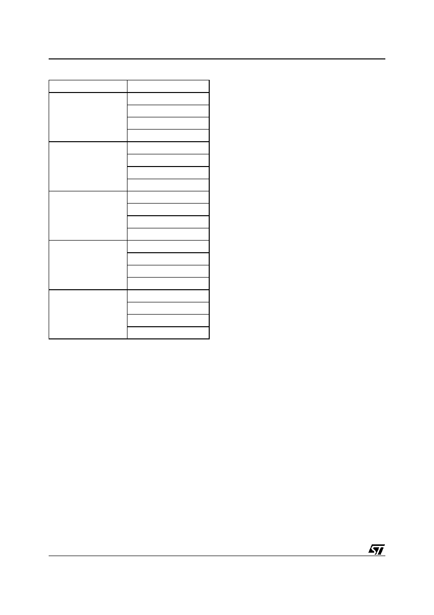
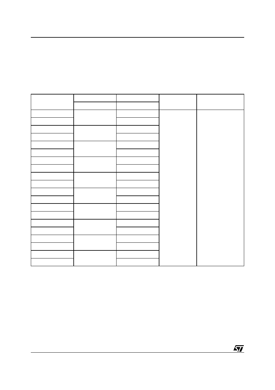
Table 2. Product Description
Note: 1. Both Single and Dual Die devices.
2. Dual Die devices only.
Figure 2. Logic Block Diagram
Reference
Part Number
Density
Bus
Width
Page
Size
Block
Size
Memory
Array
Operating
Voltage
Timings
Packages
Random
Access
(max)
Sequential
Access
(min)
Page
Program
(typ)
Block
Erase (typ)
NAND512-B
NAND512R3B
512Mbit
x8
2048+64
Bytes
128K+4K
Bytes
64 Pages x
512 Blocks
1.7 to 1.95V
25µs
60ns
300µs
2ms
TSOP48
USOP48
VFBGA63
NAND512W3B
2.7 to 3.6V
25µs
50ns
300µs
NAND512R4B
x16
1024+32
Words
64K+2K
Words
1.7 to 1.95V
25µs
60ns
300µs
NAND512W4B
2.7 to 3.6V
25µs
50ns
300µs
NAND01G-B
NAND01GR3B
1Gbit
x8
2048+64
Bytes
128K+4K
Bytes
64 Pages x
1024 Blocks
1.7 to 1.95V
25µs
60ns
300µs
2ms
TSOP48
USOP48
VFBGA63
NAND01GW3B
2.7 to 3.6V
25µs
50ns
300µs
NAND01GR4B
x16
1024+32
Words
64K+2K
Words
1.7 to 1.95V
25µs
60ns
300µs
NAND01GW4B
2.7 to 3.6V
25µs
50ns
300µs
NAND02G-B
NAND02GR3B
2Gbit
x8
2048+64
Bytes
128K+4K
Bytes
64 Pages x
2048 Blocks
1.7 to 1.95V
25µs
60ns
300µs
2ms
TSOP48
(1)
TFBGA63
(2)
NAND02GW3B
2.7 to 3.6V
25µs
50ns
300µs
NAND02GR4B
x16
1024+32
Words
64K+2K
Words
1.7 to 1.95V
25µs
60ns
300µs
NAND02GW4B
2.7 to 3.6V
25µs
50ns
300µs
NAND04G-B
NAND04GR3B
4Gbit
x8
2048+64
Bytes
128K+4K
Bytes
64 Pages x
4096 Blocks
1.7 to 1.95V
25µs
60ns
300µs
2ms
TSOP48
NAND04GW3B
2.7 to 3.6V
25µs
50ns
300µs
NAND04GR4B
x16
1024+32
Words
64K+2K
Words
1.7 to 1.95V
25µs
60ns
300µs
NAND04GW4B
2.7 to 3.6V
25µs
50ns
300µs
NAND08G-B
NAND08GR3B
8Gbit
x8
2048+64
Bytes
128K+4K
Bytes
64 Pages x
8192 Blocks
1.7 to 1.95V
25µs
60ns
300µs
2ms
TSOP48
LFBGA63
NAND08GW3B
2.7 to 3.6V
25µs
50ns
300µs
NAND08GR4B
x16
1024+32
Words
64K+2K
Words
1.7 to 1.95V
25µs
60ns
300µs
NAND08GW4B
2.7 to 3.6V
25µs
50ns
300µs
Address
Register/Counter
Command
Interface
Logic
P/E/R Controller,
High Voltage
Generator
WP
I/O Buffers & Latches
I/O8-I/O15, x16
E
W
AI09373b
R
Y Decoder
Page Buffer
NAND Flash
Memory Array
X Decoder
I/O0-I/O7, x8/x16
Command Register
CL
AL
Cache Register
RB
PRL
9/59
NAND512-B, NAND01G-B, NAND02G-B, NAND04G-B, NAND08G-B
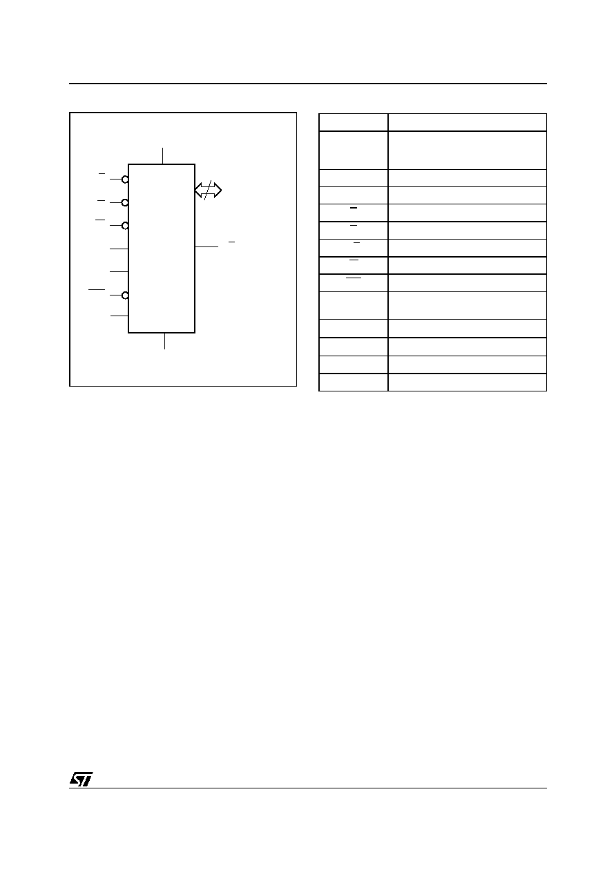
Figure 3. Logic Diagram
Table 3. Signal Names
AI09372b
W
I/O8-I/O15, x16
VDD
NAND Flash
E
VSS
WP
AL
CL
RB
R
I/O0-I/O7, x8/x16
PRL
I/O8-15
Data Input/Outputs for x16 devices
I/O0-7
Data Input/Outputs, Address Inputs,
or Command Inputs for x8 and x16
devices
AL
Address Latch Enable
CL
Command Latch Enable
E
Chip Enable
R
Read Enable
RB
Ready/Busy (open-drain output)
W
Write Enable
WP
Write Protect
PRL
Power-Up Read Enable, Lock/Unlock
Enable
V
DD
Supply Voltage
V
SS
Ground
NC
Not Connected Internally
DU
Do Not Use

NAND512-B, NAND01G-B, NAND02G-B, NAND04G-B, NAND08G-B
10/59
Figure 4. TSOP48 and USOP48 Connections,
x8 devices
Figure 5. TSOP48 and USOP48 Connections,
x16 devices
I/O3
I/O2
I/O6
R
RB
NC
I/O4
I/O7
AI09374
NAND Flash
(x8)
12
1
13
24
25
36
37
48
E
I/O1
NC
NC
NC
NC
NC
NC
NC
WP
W
NC
NC
NC
VSS
VDD
AL
NC
NC
CL
NC
I/O5
NC
NC
NC
I/O0
NC
NC
NC
NC
PRL
VDD
NC
NC
NC
VSS
NC
NC
NC
NC
I/O3
I/O9
I/O2
I/O6
R
RB
NC
I/O14
I/O12
I/O10
I/O4
I/O7
AI09375
NAND Flash
(x16)
12
1
13
24
25
36
37
48
I/O8
E
I/O1
I/O11
NC
NC
NC
NC
NC
NC
NC
WP
W
NC
NC
NC
VSS
VDD
AL
NC
NC
CL
NC
I/O13
I/O15
I/O5
VSS
NC
VSS
I/O0
NC
PRL
NC
NC
NC
VDD
11/59
NAND512-B, NAND01G-B, NAND02G-B, NAND04G-B, NAND08G-B
Figure 6. FBGA63 Connections, x8 devices (Top view through package)
AI09376
I/O7
WP
I/O4
I/O3
NC
VDD
I/O5
VDD
NC
H
VSS
I/O6
D
E
CL
C
NC
NC
B
DU
NC
W
NC
A
8
7
6
5
4
3
2
1
NC
NC
NC
NC
G
F
E
I/O0
AL
DU
NC
NC
NC
NC
NC
NC
NC
NC
NC
NC
VSS
NC
NC
NC
NC
RB
I/O2
DU
NC
DU
I/O1
10
9
R
NC
PRL
NC
VSS
DU
DU
DU
DU
DU
DU
DU
DU
DU
DU
DU
M
L
K
J
NAND512-B, NAND01G-B, NAND02G-B, NAND04G-B, NAND08G-B
12/59
Figure 7. FBGA63 Connections, x16 devices (Top view through package)
AI09377
I/O15
WP
I/O4
I/O11
I/O10
VDD
I/O6
VDD
I/O3
H
VSS
I/O13
D
E
CL
C
NC
NC
B
DU
NC
W
NC
A
8
7
6
5
4
3
2
1
NC
NC
NC
NC
G
F
E
I/O1
AL
DU
NC
NC
NC
NC
NC
NC
I/O7
I/O5
I/O14
I/O12
VSS
NC
NC
NC
NC
RB
I/O2
DU
I/O0
DU
I/O9
10
9
R
NC
PRL
I/O8
VSS
DU
DU
DU
DU
DU
DU
DU
DU
DU
DU
DU
M
L
K
J

13/59
NAND512-B, NAND01G-B, NAND02G-B, NAND04G-B, NAND08G-B
MEMORY ARRAY ORGANIZATION
The memory array is made up of NAND structures
where 32 cells are connected in series.
The memory array is organized in blocks where
each block contains 64 pages. The array is split
into two areas, the main area and the spare area.
The main area of the array is used to store data
whereas the spare area is typically used to store
Error correction Codes, software flags or Bad
Block identification.
In x8 devices the pages are split into a 2048 Byte
main area and a spare area of 64 Bytes. In the x16
devices the pages are split into a 1,024 Word main
area and a 32 Word spare area. Refer to
Figure
8., Memory Array Organization
.
Bad Blocks
The NAND Flash 2112 Byte/ 1056 Word Page de-
vices may contain Bad Blocks, that is blocks that
contain one or more invalid bits whose reliability is
not guaranteed. Additional Bad Blocks may devel-
op during the lifetime of the device.
The Bad Block Information is written prior to ship-
ping (refer to
Bad Block Management
section for
more details).
Table 4.
shows the minimum number of valid
blocks in each device. The values shown include
both the Bad Blocks that are present when the de-
vice is shipped and the Bad Blocks that could de-
velop later on.
These blocks need to be managed using Bad
Blocks Management, Block Replacement or Error
Correction Codes (refer to
SOFTWARE ALGO-
RITHMS
section).
Table 4. Valid Blocks
Figure 8. Memory Array Organization
Density of Device
Min
Max
8 Gbits
8032
8192
4 Gbits
4016
4096
2 Gbits
2008
2048
1Gbit
1004
1024
512 Mbits
502
512
AI09854
Block = 64 Pages
Page = 2112 Bytes (2,048 + 64)
2,048 Bytes
2048 Bytes
Spare Area
64
Bytes
Block
8 bits
64
Bytes
8 bits
Page
Page Buffer, 2112 Bytes
Block = 64 Pages
Page = 1056 Words (1024 + 32)
1,024 Words
1024 Words
Spare Area
Main Area
32
Words
16 bits
32
Words
16 bits
Page Buffer, 1056 Words
Block
Page
x8 DEVICES
x16 DEVICES
Main Area

NAND512-B, NAND01G-B, NAND02G-B, NAND04G-B, NAND08G-B
14/59
SIGNAL DESCRIPTIONS
See
Figure 3., Logic Diagram
, and
Table
3., Signal Names
, for a brief overview of the sig-
nals connected to this device.
Inputs/Outputs (I/O0-I/O7). Input/Outputs 0 to 7
are used to input the selected address, output the
data during a Read operation or input a command
or data during a Write operation. The inputs are
latched on the rising edge of Write Enable. I/O0-I/
O7 are left floating when the device is deselected
or the outputs are disabled.
Inputs/Outputs (I/O8-I/O15). Input/Outputs 8 to
15 are only available in x16 devices. They are
used to output the data during a Read operation or
input data during a Write operation. Command and
Address Inputs only require I/O0 to I/O7.
The inputs are latched on the rising edge of Write
Enable. I/O8-I/O15 are left floating when the de-
vice is deselected or the outputs are disabled.
Address Latch Enable (AL). The Address Latch
Enable activates the latching of the Address inputs
in the Command Interface. When AL is high, the
inputs are latched on the rising edge of Write En-
able.
Command Latch Enable (CL). The Command
Latch Enable activates the latching of the Com-
mand inputs in the Command Interface. When CL
is high, the inputs are latched on the rising edge of
Write Enable.
Chip Enable (E). The Chip Enable input acti-
vates the memory control logic, input buffers, de-
coders and sense amplifiers. When Chip Enable is
low, V
IL
, the device is selected. If Chip Enable
goes high, v
IH
, while the device is busy, the device
remains selected and does not go into standby
mode.
Read Enable (R). The Read Enable pin, R, con-
trols the sequential data output during Read oper-
ations. Data is valid t
RLQV
after the falling edge of
R. The falling edge of R also increments the inter-
nal column address counter by one.
Power-Up Read Enable, Lock/Unlock Enable
(PRL). The Power-Up Read Enable, Lock/Unlock
Enable input, PRL, is used to enable and disable
the lock mechanism, and the Automatic Page 0
Read at Power-up option. When PRL is High, V
IH
,
the device is in Block Lock mode and the Automat-
ic Page 0 Read at Power-Up option is enabled.
The Automatic Page 0 Read at Power-Up option is
available in 3.3V devices only.
If the Power-Up Read Enable, Lock/Unlock En-
able input is not required, the PRL pin should be
left unconnected (Not Connected) or connected to
V
SS
.
Write Enable (W). The Write Enable input, W,
controls writing to the Command Interface, Input
Address and Data latches. Both addresses and
data are latched on the rising edge of Write En-
able.
During power-up and power-down a recovery time
of 1µs (min) is required before the Command Inter-
face is ready to accept a command. It is recom-
mended to keep Write Enable high during the
recovery time.
Write Protect (WP). The Write Protect pin is an
input that gives a hardware protection against un-
wanted program or erase operations. When Write
Protect is Low, V
IL
, the device does not accept any
program or erase operations.
It is recommended to keep the Write Protect pin
Low, V
IL
, during power-up and power-down.
Ready/Busy (RB). The Ready/Busy output, RB,
is an open-drain output that can be used to identify
if the P/E/R Controller is currently active.
When Ready/Busy is Low, V
OL
, a read, program or
erase operation is in progress. When the operation
completes Ready/Busy goes High, V
OH
.
The use of an open-drain output allows the Ready/
Busy pins from several memories to be connected
to a single pull-up resistor. A Low will then indicate
that one, or more, of the memories is busy.
Refer to the
Ready/Busy Signal Electrical Charac-
teristics
section for details on how to calculate the
value of the pull-up resistor.
V
DD
Supply Voltage. V
DD
provides the power
supply to the internal core of the memory device.
It is the main power supply for all operations (read,
program and erase).
An internal voltage detector disables all functions
whenever V
DD
is below 2.5V (for 3V devices) or
1.5V (for 1.8V devices) to protect the device from
any involuntary program/erase during power-tran-
sitions.
Each device in a system should have V
DD
decou-
pled with a 0.1µF capacitor. The PCB track widths
should be sufficient to carry the required program
and erase currents
V
SS
Ground. Ground, V
SS,
is the reference for
the power supply. It must be connected to the sys-
tem ground.
15/59
NAND512-B, NAND01G-B, NAND02G-B, NAND04G-B, NAND08G-B
BUS OPERATIONS
There are six standard bus operations that control
the memory. Each of these is described in this
section, see
Table 5., Bus Operations
, for a sum-
mary.
Typically, glitches of less than 5 ns on Chip En-
able, Write Enable and Read Enable are ignored
by the memory and do not affect bus operations.
Command Input
Command Input bus operations are used to give
commands to the memory. Commands are ac-
cepted when Chip Enable is Low, Command Latch
Enable is High, Address Latch Enable is Low and
Read Enable is High. They are latched on the ris-
ing edge of the Write Enable signal.
Only I/O0 to I/O7 are used to input commands.
See
Figure 25.
and
Table 24.
for details of the tim-
ings requirements.
Address Input
Address Input bus operations are used to input the
memory addresses. Four bus cycles are required
to input the addresses for the 512Mb and 1Gb de-
vices whereas five bus cycles are required for the
2Gb, 4Gb and 8Gb devices (refer to
Table 6.
and
Table 7.
, Address Insertion).
The addresses are accepted when Chip Enable is
Low, Address Latch Enable is High, Command
Latch Enable is Low and Read Enable is High.
They are latched on the rising edge of the Write
Enable signal. Only I/O0 to I/O7 are used to input
addresses.
See
Figure 26.
and
Table 24.
for details of the tim-
ings requirements.
Data Input
Data Input bus operations are used to input the
data to be programmed.
Data is accepted only when Chip Enable is Low,
Address Latch Enable is Low, Command Latch
Enable is Low and Read Enable is High. The data
is latched on the rising edge of the Write Enable
signal. The data is input sequentially using the
Write Enable signal.
See
Figure 27.
and
Table 24.
and
Table 25.
for de-
tails of the timings requirements.
Data Output
Data Output bus operations are used to read: the
data in the memory array, the Status Register, the
lock status, the Electronic Signature
and the
Unique Identifier.
Data is output when Chip Enable is Low, Write En-
able is High, Address Latch Enable is Low, and
Command Latch Enable is Low.
The data is output sequentially using the Read En-
able signal.
See
Figure 28.
and
Table 25.
for details of the tim-
ings requirements.
Write Protect
Write Protect bus operations are used to protect
the memory against program or erase operations.
When the Write Protect signal is Low the device
will not accept program or erase operations and so
the contents of the memory array cannot be al-
tered. The Write Protect signal is not latched by
Write Enable to ensure protection even during
power-up.
Standby
When Chip Enable is High the memory enters
Standby mode, the device is deselected, outputs
are disabled and power consumption is reduced.
Table 5. Bus Operations
Note: 1. Only for x16 devices.
2. WP must be V
IH
when issuing a program or erase command.
Bus Operation
E
AL
CL
R
W
WP
I/O0 - I/O7
I/O8 - I/O15
(1)
Command Input
V
IL
V
IL
V
IH
V
IH
Rising
X
(2)
Command
X
Address Input
V
IL
V
IH
V
IL
V
IH
Rising
X
Address
X
Data Input
V
IL
V
IL
V
IL
V
IH
Rising
V
IH
Data Input
Data Input
Data Output
V
IL
V
IL
V
IL
Falling
V
IH
X
Data Output
Data Output
Write Protect
X
X
X
X
X
V
IL
X
X
Standby
V
IH
X
X
X
X
V
IL
/V
DD
X
X

NAND512-B, NAND01G-B, NAND02G-B, NAND04G-B, NAND08G-B
16/59
Table 6. Address Insertion, x8 Devices
Note: 1. Any additional address input cycles will be ignored.
2. The fifth cycle is valid for 2Gb, 4Gb and 8Gb devices. A28 is for 2Gb devices, A29-A28 are for 4Gb devices and A30-A28 for 8Gb
devices only.
Table 7. Address Insertion, x16 Devices
Note: 1. Any additional address input cycles will be ignored.
2. The fifth cycle is valid for 2Gb, 4Gb and 8Gb devices. A27 is for 2Gb devices, A28-A27 are for 4Gb devices and A29-A27 for 8Gb
devices.
Bus Cycle
I/O7
I/O6
I/O5
I/O4
I/O3
I/O2
I/O1
I/O0
1
st
A7
A6
A5
A4
A3
A2
A1
A0
2
nd
V
IL
V
IL
V
IL
V
IL
A11
A10
A9
A8
3
rd
A19
A18
A17
A16
A15
A14
A13
A12
4
th
A27
A26
A25
A24
A23
A22
A21
A20
5
th(2)
V
IL
V
IL
V
IL
V
IL
V
IL
A30
A29
A28
Bus
Cycle
I/O8-
I/O15
I/O7
I/O6
I/O5
I/O4
I/O3
I/O2
I/O1
I/O0
1
st
X
A7
A6
A5
A4
A3
A2
A1
A0
2
nd
X
V
IL
V
IL
V
IL
V
IL
V
IL
A10
A9
A8
3
rd
X
A18
A17
A16
A15
A14
A13
A12
A11
4
th
X
A26
A25
A24
A23
A22
A21
A20
A19
5
th(2)
X
V
IL
V
IL
V
IL
V
IL
V
IL
A29
A28
A27

17/59
NAND512-B, NAND01G-B, NAND02G-B, NAND04G-B, NAND08G-B
Table 8. Address Definitions, x8
Table 9. Address Definitions, x16
Address
Definition
A0 - A11
Column Address
A12 - A17
Page Address
A18 - A26
Block Address
512Mb device
A18 - A27
Block Address
1Gb device
A18 - A28
Block Address
2Gb device
A18 - A29
Block Address
4Gb device
A18 - A30
Block Address
8Gb device
Address
Definition
A0 - A10
Column Address
A11 - A16
Page Address
A17 - A25
Block Address
512Mb device
A17 - A26
Block Address
1Gb device
A17 - A27
Block Address
2Gb device
A17 - A28
Block Address
4Gb device
A17 - A29
Block Address
8Gb device
NAND512-B, NAND01G-B, NAND02G-B, NAND04G-B, NAND08G-B
18/59
COMMAND SET
All bus write operations to the device are interpret-
ed by the Command Interface. The Commands
are input on I/O0-I/O7 and are latched on the rising
edge of Write Enable when the Command Latch
Enable signal is high. Device operations are se-
lected by writing specific commands to the Com-
mand Register. The two-step command
sequences for program and erase operations are
imposed to maximize data security.
The Commands are summarized in
Table
10., Commands
.
Table 10. Commands
Note: 1. The bus cycles are only shown for issuing the codes. The cycles required to input the addresses or input/output data are not shown.
2. For consecutive read operations the 00h command does not need to be repeated.
3. Only during Cache Read busy.
Command
Bus Write Operations
(1)
Commands
accepted
during busy
1
st
CYCLE
2
nd
CYCLE
3
rd
CYCLE
4
th
CYCLE
Read
00h
(2)
30h
≠
≠
Random Data Output
05h
E0h
≠
≠
Cache Read
00h
31h
≠
≠
Exit Cache Read
34h
≠
≠
≠
Yes
(5)
Page Program
(Sequential Input default)
80h
10h
≠
≠
Random Data Input
85h
≠
≠
≠
Copy Back Program
00h
35h
85h
10h
Cache Program
80h
15h
≠
≠
Block Erase
60h
D0h
≠
≠
Reset
FFh
≠
≠
≠
Yes
Read Electronic Signature
90h
≠
≠
≠
Read Status Register
70h
≠
≠
≠
Yes
Read Block Lock Status
7Ah
≠
≠
≠
Blocks Unlock
23h
24h
≠
≠
Blocks Lock
2Ah
≠
≠
≠
Blocks Lock-Down
2Ch
≠
≠
≠

19/59
NAND512-B, NAND01G-B, NAND02G-B, NAND04G-B, NAND08G-B
DEVICE OPERATIONS
The following section gives the details of the de-
vice operations.
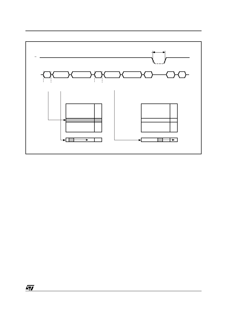
Read Memory Array
At Power-Up the device defaults to Read mode.
To enter Read mode from another mode the Read
command must be issued, see
Table
10., Commands
. Once a Read command is is-
sued, subsequent consecutive Read commands
only require the confirm command code (30h).
Once a Read command is issued two types of op-
erations are available: Random Read and Page
Read.
Random Read. Each time the Read command is
issued the first read is Random Read.
Page Read. After the first Random Read access,
the page data (2112 Bytes or 1056 Words) is
transferred to the Page Buffer in a time of
t
WHBH
(refer to
Table 25.
for value). Once the transfer is
complete the Ready/Busy signal goes High. The
data can then be read out sequentially (from se-
lected column address to last column address) by
pulsing the Read Enable signal.
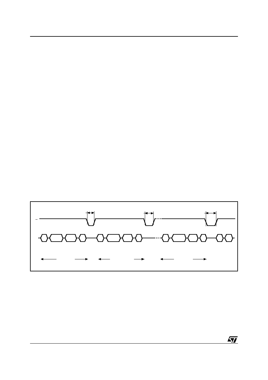
The device can output random data in a page, in-
stead of the consecutive sequential data, by issu-
ing a Random Data Output command.
The Random Data Output command can be used
to skip some data during a sequential data output.
The sequential operation can be resumed by
changing the column address of the next data to
be output, to the address which follows the Ran-
dom Data Output command.
The Random Data Output command can be is-
sued as many times as required within a page.
The Random Data Output command is not accept-
ed during Cache Read operations.
Figure 9. Read Operations
Note: 1. Highest address depends on device density.
CL
E
W
AL
R
I/O
RB
00h
ai08657b
Busy
Command
Code
Data Output (sequentially)
Address Input
tBLBH1
30h
Command
Code

NAND512-B, NAND01G-B, NAND02G-B, NAND04G-B, NAND08G-B
20/59
Figure 10. Random Data Output During Sequential Data Output
I/O
RB
Address
Inputs
ai08658
Data Output
Busy
tBLBH1
(Read Busy time)
00h
Cmd
Code
30h
Address
Inputs
Data Output
05h
E0h
5 Add cycles
Main Area
Spare
Area
Col Add 1,2
Row Add 1,2,3
Cmd
Code
Cmd
Code
Cmd
Code
2Add cycles
Main Area
Spare
Area
Col Add 1,2
R
21/59
NAND512-B, NAND01G-B, NAND02G-B, NAND04G-B, NAND08G-B
Cache Read
The Cache Read operation is used to improve the
read throughput by reading data using the Cache
Register. As soon as the user starts to read one
page, the device automatically loads the next page
into the Cache Register.
An Cache Read operation consists of three steps
(see
Table 10.
):
1.
One bus cycle is required to setup the Cache
Read command (the same as the standard
Read command)
2.
Four or Five (refer to
Table 6.
and
Table 7.
)
bus cycles are then required to input the Start
Address
3.
One bus cycle is required to issue the Cache
Read confirm command to start the P/E/R
Controller.
The Start Address must be at the beginning of a
page (Column Address = 00h, see
Table 8.
and
Table 9.
). This allows the data to be output unin-
terrupted after the latency time (t
BLBH1
), see
Fig-
ure 11.
The Ready/Busy signal can be used to monitor the
start of the operation. During the latency period the
Ready/Busy signal goes Low, after this the Ready/
Busy signal goes High, even if the device is inter-
nally downloading page n+1.
Once the Cache Read operation has started, the
Status Register can be read using the Read Status
Register command.
During the operation, SR5 can be read, to find out
whether the internal reading is ongoing (SR5 =
`0'), or has completed (SR5 = `1'), while SR6 indi-
cates whether the Cache Register is ready to
download new data.
To exit the Cache Read operation an Exit Cache
Read command must be issued (see
Table 10.
).
If the Exit Cache Read command is issued while
the device is internally reading page n+1, page n
will still be output, but not page n+1.
Figure 11. Cache Read Operation
I/O
RB
Address
Inputs
ai08661
00h
Read
Setup
Code
31h
Cache
Read
Confirm
Code
Busy
tBLBH1
(Read Busy time)
1st page
Data Output
2nd page
3rd page
last page
34h
Exit
Cache
Read
Code
Block N

NAND512-B, NAND01G-B, NAND02G-B, NAND04G-B, NAND08G-B
22/59
Page Program
The Page Program operation is the standard oper-
ation to program data to the memory array. Gener-
ally, data is programmed sequentially, however
the device does support Random Input within a
page.
The memory array is programmed by page, how-
ever partial page programming is allowed where
any number of Bytes (1 to 2112) or Words (1 to
1056) can be programmed.
The maximum number of consecutive partial page
program operations allowed in the same page is
eight. After exceeding this a Block Erase com-
mand must be issued before any further program
operations can take place in that page.
Sequential Input. To input data sequentially the
addresses must be sequential and remain in one
block.
For Sequential Input each Page Program opera-
tion consists of five steps (see
Figure 12.
):
1.
one bus cycle is required to setup the Page
Program (Sequential Input) command (see
Table 10.
)
2.
four or five bus cycles are then required to
input the program address (refer to
Table 6.
and
Table 7.
)
3.
the data is then loaded into the Data Registers
4.
one bus cycle is required to issue the Page
Program confirm command to start the P/E/R
Controller. The P/E/R will only start if the data
has been loaded in step 3.
5.
the P/E/R Controller then programs the data
into the array.
Random Data Input. During a Sequential Input
operation, the next sequential address to be pro-
grammed can be replaced by a random address,
by issuing a Random Data Input command. The
following two steps are required to issue the com-
mand:
1.
one bus cycle is required to setup the Random
Data Input command (see
Table 10.
)
2.
two bus cycles are then required to input the
new column address (refer to
Table 6.
)
Random Data Input can be repeated as often as
required in any given page.
Once the program operation has started the Sta-
tus Register can be read using the Read Status
Register command. During program operations
the Status Register will only flag errors for bits set
to '1' that have not been successfully programmed
to '0'.
During the program operation, only the Read Sta-
tus Register and Reset commands will be accept-
ed, all other commands will be ignored.
Once the program operation has completed the P/
E/R Controller bit SR6 is set to `1' and the Ready/
Busy signal goes High.
The device remains in Read Status Register mode
until another valid command is written to the Com-
mand Interface.
Figure 12. Page Program Operation
I/O
RB
Address Inputs
SR0
ai08659
Data Input
10h
70h
80h
Page Program
Setup Code
Confirm
Code
Read Status Register
Busy
tBLBH2
(Program Busy time)
23/59
NAND512-B, NAND01G-B, NAND02G-B, NAND04G-B, NAND08G-B
Figure 13. Random Data Input During Sequential Data Input
I/O
Address
Inputs
ai08664
Data Intput
80h
Cmd
Code
Address
Inputs
Data Input
85h
5 Add cycles
Main Area
Spare
Area
Col Add 1,2
Row Add 1,2,3
Cmd
Code
2 Add cycles
Main Area
Spare
Area
Col Add 1,2
RB
Busy
tBLBH2
(Program Busy time)
SR0
10h
70h
Confirm
Code
Read Status Register
NAND512-B, NAND01G-B, NAND02G-B, NAND04G-B, NAND08G-B
24/59
Copy Back Program
The Copy Back Program operation is used to copy
the data stored in one page and reprogram it in an-
other page.
The Copy Back Program operation does not re-
quire external memory and so the operation is
faster and more efficient because the reading and
loading cycles are not required. The operation is
particularly useful when a portion of a block is up-
dated and the rest of the block needs to be copied
to the newly assigned block.
If the Copy Back Program operation fails an error
is signalled in the Status Register. However as the
standard external ECC cannot be used with the
Copy Back Program operation bit error due to
charge loss cannot be detected. For this reason it
is recommended to limit the number of Copy Back
Program operations on the same data and or to
improve the performance of the ECC.
The Copy Back Program operation requires four
steps:
1.
The first step reads the source page. The
operation copies all 1056 Words/ 2112 Bytes
from the page into the Data Buffer. It requires:
≠
one bus write cycle to setup the command
≠
4 bus write cycles to input the source page
address
≠
one bus write cycle to issue the confirm
command code
2.
When the device returns to the ready state
(Ready/Busy High), the next bus write cycle of
the command is given with the 4 bus cycles to
input the target page address. Refer to
Table
11.
for the addresses that must be the same
for the Source and Target pages.
3.
Then the confirm command is issued to start
the P/E/R Controller.
The Data Input cycle for modifying the source
page is performed as shown in
Figure 14.
After a
Copy Back Program operation, a partial-page pro-
gram is not allowed in the target page until the
block has been erased.
See
Figure 14.
for an example of the Copy Back
Program operation.
A data input cycle to modify a portion or a multiple
distant portion of the source page, is shown in
Fig-
ure 15.
Table 11. Copy Back Program x8 Addresses
Note: 1. DD = Dual Die, QD = Quadruple Die.
Table 12. Copy Back Program x16 Addresses
Note: 1. DD = Dual Die, QD = Quadruple Die.
Density
Same Address for Source and
Target Pages
512 Mbit
no constraint
1 Gbit
no constraint
2 Gbit DD
(1)
A28
2 Gbit
no constraint
4 Gbit DD
A29
8 Gbit QD
(1)
A29,A30
Density
Same Address for Source and
Target Pages
512 Mbit
no constraint
1 Gbit
no constraint
2 Gbit DD
(1)
A27
2 Gbit
no constraint
4 Gbit DD
(1)
A28
8 Gbit QD
(1)
A28,A29

25/59
NAND512-B, NAND01G-B, NAND02G-B, NAND04G-B, NAND08G-B
Figure 14. Copy Back Program
Figure 15. Page Copy Back Program with Random Data Input
I/O
RB
Source
Add Inputs
ai09858b
85h
Copy Back
Code
Read
Code
Read Status Register
Target
Add Inputs
tBLBH1
(Read Busy time)
Busy
tBLBH2
(Program Busy time)
00h
10h
70h
SR0
Busy
35h
I/O
RB
Source
Add Inputs
ai11001
85h
Read
Code
Target
Add Inputs
tBLBH1
(Read Busy time)
00h
Busy
35h
85h
Data
2 Cycle
Add Inputs
Data
Copy Back
Code
10h
70h
Unlimited number of repetitions
Busy
tBLBH2
(Program Busy time)
SR0
NAND512-B, NAND01G-B, NAND02G-B, NAND04G-B, NAND08G-B
26/59
Cache Program
The Cache Program operation is used to improve
the programming throughput by programming
data using the Cache Register. The Cache Pro-
gram operation can only be used within one block.
The Cache Register allows new data to be input
while the previous data that was transferred to the
Page Buffer is programmed into the memory ar-
ray.
Each Cache Program operation consists of five
steps (refer to
Figure 16.
):
1.
First of all the program setup command is
issued (one bus cycle to issue the program
setup command then four bus write cycles to
input the address), the data is then input (up to
2112 Bytes/ 1056 Words) and loaded into the
Cache Register.
2.
One bus cycle is required to issue the confirm
command to start the P/E/R Controller.
3.
The P/E/R Controller then transfers the data to
the
Page Buffer. During this the device is busy
for a time of t
WHBH2
.
4.
Once the data is loaded into the Page Buffer
the P/E/R Controller programs the data into
the memory array. As soon as the Cache
Registers are empty (after t
WHBH2
) a new
Cache program command can be issued,
while the internal programming is still
executing.
Once the program operation has started the Sta-
tus Register can be read using the Read Status
Register command. During Cache Program oper-
ations SR5 can be read to find out whether the in-
ternal programming is ongoing (SR5 = `0') or has
completed (SR5 = `1') while SR6 indicates wheth-
er the Cache Register is ready to accept new data.
If any errors have been detected on the previous
page (
Page N-1
), the Cache Program Error Bit SR1
will be set to `1', while if the error has been detect-
ed on Page N the Error Bit SR0 will be set to '1'.
When the next page (Page N) of data is input with
the Cache Program command, t
WHBH2
is affected
by the pending internal programming. The data will
only be transferred from the Cache Register to the
Page Buffer when the pending program cycle is
finished and the Page Buffer is available.
If the system monitors the progress of the opera-
tion using only the Ready/Busy signal, the last
page of data must be programmed with the Page
Program confirm command (10h).
If the Cache Program confirm command (15h) is
used instead, Status Register bit SR5 must be
polled to find out if the last programming is finished
before starting any other operations.
Figure 16. Cache Program Operation
Note: 1. Up to 64 pages can be programmed in one Cache Program operation.
2. t
CACHEPG
is the program time for the last page + the program time for the (last
-
1)
th
page
-
(Program command cycle time + Last
page data loading time).
I/O
RB
Address
Inputs
ai08672
80h
Page
Program
Code
Read Status
Register
Busy
Data
Inputs
15h
Cache
Program
Code
80h
Page
Program
Code
15h
Cache Program
Confirm Code
Busy
Last Page
tBLBH5
(Cache Busy time)
tBLBH5
tCACHEPG
SR0
70h
80h
10h
Page
Program
Confirm Code
Busy
First Page
Second Page
(can be repeated up to 63 times)
Address
Inputs
Data
Inputs
Address
Inputs
Data
Inputs

27/59
NAND512-B, NAND01G-B, NAND02G-B, NAND04G-B, NAND08G-B
Block Erase
Erase operations are done one block at a time. An
erase operation sets all of the bits in the ad-
dressed block to `1'. All previous data in the block
is lost.
An erase operation consists of three steps (refer to
Figure 17.
):
1.
One bus cycle is required to setup the Block
Erase command. Only addresses A18-A27
(x8) or A17-A26 (x16) are used, the other
address inputs are ignored.
2.
two or three bus cycles are then required to
load the address of the block to be erased.
Refer to
Table 8.
and
Table 9.
for the block
addresses of each device.
3.
one bus cycle is required to issue the Block
Erase confirm command to start the P/E/R
Controller.
The operation is initiated on the rising edge of
write Enable, W, after the confirm command is is-
sued. The P/E/R Controller handles Block Erase
and implements the verify process.
During the Block Erase operation, only the Read
Status Register and Reset commands will be ac-
cepted, all other commands will be ignored.
Once the program operation has completed the P/
E/R Controller bit SR6 is set to `1' and the Ready/
Busy signal goes High. If the operation completed
successfully, the Write Status Bit SR0 is `0', other-
wise it is set to `1'.
Figure 17. Block Erase Operation
Reset
The Reset command is used to reset the Com-
mand Interface and Status Register. If the Reset
command is issued during any operation, the op-
eration will be aborted. If it was a program or erase
operation that was aborted, the contents of the
memory locations being modified will no longer be
valid as the data will be partially programmed or
erased.
If the device has already been reset then the new
Reset command will not be accepted.
The Ready/Busy signal goes Low for t
BLBH4
after
the Reset command is issued. The value of t
BLBH4
depends on the operation that the device was per-
forming when the command was issued, refer to
Table 25.
for the values.
I/O
RB
Block Address
Inputs
SR0
ai07593
D0h
70h
60h
Block Erase
Setup Code
Confirm
Code
Read Status Register
Busy
tBLBH3
(Erase Busy time)

NAND512-B, NAND01G-B, NAND02G-B, NAND04G-B, NAND08G-B
28/59
Read Status Register
The device contains a Status Register which pro-
vides information on the current or previous Pro-
gram or Erase operation. The various bits in the
Status Register convey information and errors on
the operation.
The Status Register is read by issuing the Read
Status Register command. The Status Register in-
formation is present on the output data bus (I/O0-
I/O7) on the falling edge of Chip Enable or Read
Enable, whichever occurs last. When several
memories are connected in a system, the use of
Chip Enable and Read Enable signals allows the
system to poll each device separately, even when
the Ready/Busy pins are common-wired. It is not
necessary to toggle the Chip Enable or Read En-
able signals to update the contents of the Status
Register.
After the Read Status Register command has
been issued, the device remains in Read Status
Register mode until another command is issued.
Therefore if a Read Status Register command is
issued during a Random Read cycle a new Read
command must be issued to continue with a Page
Read operation.
The Status Register bits are summarized in
Table
13., Status Register Bits
, . Refer to
Table 13.
in
conjunction with the following text descriptions.
Write Protection Bit (SR7). The Write Protection
bit can be used to identify if the device is protected
or not. If the Write Protection bit is set to `1' the de-
vice is not protected and program or erase opera-
tions are allowed. If the Write Protection bit is set
to `0' the device is protected and program or erase
operations are not allowed.
P/E/R Controller and Cache Ready/Busy Bit
(SR6). Status Register bit SR6 has two different
functions depending on the current operation.
During Cache Program operations SR6 acts as a
Cache Program Ready/Busy bit, which indicates
whether the Cache Register is ready to accept
new data. When SR6 is set to '0', the Cache Reg-
ister is busy and when SR6 is set to '1', the Cache
Register is ready to accept new data.
During all other operations SR6 acts as a P/E/R Con-
troller bit, which indicates whether the P/E/R Con-
troller is active or inactive. When the P/E/R
Controller bit is set to `0', the P/E/R Controller is
active (device is busy); when the bit is set to `1', the
P/E/R Controller is inactive (device is ready).
P/E/R Controller Bit (SR5). The Program/Erase/
Read Controller bit indicates whether the P/E/R
Controller is active or inactive. When the P/E/R
Controller bit is set to `0', the P/E/R Controller is
active (device is busy); when the bit is set to `1', the
P/E/R Controller is inactive (device is ready).
Cache Program Error Bit (SR1). The Cache Pro-
gram Error bit can be used to identify if the previous
page (page N-1) has been successfully pro-
gramed or not in a Cache Program operation. SR1
is set to '1' when the Cache Program operation
has failed to program the previous page (page N-
1) correctly. If SR1 is set to `0' the operation has
completed successfully.
The Cache Program Error bit is only valid during
Cache Program operations, during other opera-
tions it is Don't Care.
Error Bit (SR0). The Error bit is used to identify if
any errors have been detected by the P/E/R Con-
troller. The Error Bit is set to '1' when a program or
erase operation has failed to write the correct data
to the memory. If the Error Bit is set to `0' the oper-
ation has completed successfully. The Error Bit
SR0, in a Cache Program operation, indicates a
failure on Page N.
SR4, SR3 and SR2 are Reserved.
29/59
NAND512-B, NAND01G-B, NAND02G-B, NAND04G-B, NAND08G-B
Table 13. Status Register Bits
Note: 1. The SR6 bit and SR0 bit have a different meaning during Cache Program and Cache Read operations.
2. Only valid for Cache Program operations, for other operations it is same as SR6.
3. Only valid for Cache Program operations, for other operations it is Don't Care.
Bit
Name
Logic Level
Definition
SR7
Write Protection
'1'
Not Protected
'0'
Protected
SR6
(1)
Program/ Erase/ Read
Controller
'1'
P/E/R C inactive, device ready
'0'
P/E/R C active, device busy
Cache Ready/Busy
'1'
Cache Register ready (Cache Program only)
'0'
Cache Register busy (Cache Program only)
SR5
Program/ Erase/ Read
Controller
(2)
'1'
P/E/R C inactive, device ready
'0'
P/E/R C active, device busy
SR4, SR3, SR2
Reserved
Don't Care
SR1
Cache Program Error
(3)
'1'
Page N-1 failed in Cache Program operation
'0'
Page N-1 programmed successfully
SR0
(1)
Generic Error
`1'
Error ≠ operation failed
`0'
No Error ≠ operation successful
Cache Program Error
`1'
Page N failed in Cache Program operation
`0'
Page N programmed successfully
NAND512-B, NAND01G-B, NAND02G-B, NAND04G-B, NAND08G-B
30/59
Read Electronic Signature
The device contains a Manufacturer Code and De-
vice Code. To read these codes three steps are re-
quired:
1.
one Bus Write cycle to issue the Read
Electronic Signature command (90h)
2.
one Bus Write cycle to input the address (00h)
3.
four Bus Read Cycles to sequentially output
the data (as shown in
Table 14., Electronic
Signature
).
Table 14. Electronic Signature
Part Number
Byte/Word 1
Byte/Word 2
Byte/Word 3
Byte/Word 4
Manufacturer Code
Device code
NAND512R3B
20h
A2h
Reserved
00h
Page Size
Spare Area size
Sequential Access Time
Block Size
Organization
(see
Table 15.
)
NAND512W3B
F2h
NAND512R4B
0020h
B2h
NAND512W4B
C2h
NAND01GR3B
20h
A1h
NAND01GW3B
F1h
NAND01GR4B
0020h
B1h
NAND01GW4B
C1h
NAND02GR3B
20h
AAh
NAND02GW3B
DAh
NAND02GR4B
0020h
BAh
NAND02GW4B
CAh
NAND04GR3B
20h
ACh
NAND04GW3B
DCh
NAND04GR4B
0020h
BCh
NAND04GW4B
CCh
NAND08GR3B
20h
A3h
NAND08GW3B
D3h
NAND08GR4B
0020h
B3h
NAND08GW4B
C3h

31/59
NAND512-B, NAND01G-B, NAND02G-B, NAND04G-B, NAND08G-B
Table 15. Electronic Signature Byte/Word 4
I/O
Definition
Value
Description
I/O1-I/O0
Page Size
(Without Spare Area)
0 0
0 1
1 0
1 1
1K
2K
Reserved
Reserved
I/O2
Spare Area Size
(Byte / 512 Byte)
0
1
8
16
I/O3
Sequential Access Time
0
1
Standard (50 ns)
Fast (30 ns)
I/O5-I/O4
Block Size
(Without Spare Area)
0 0
0 1
1 0
1 1
64K
128K
256K
Reserved
I/O6
Organization
0
1
X8
X16
I/O7
Not Used
Reserved
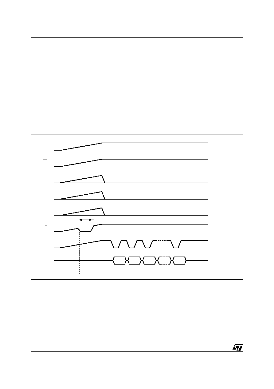
NAND512-B, NAND01G-B, NAND02G-B, NAND04G-B, NAND08G-B
32/59
Automatic Page 0 Read at Power-Up
The 3V devices (NANDxxxWxB) feature Automat-
ic Page 0 Read at Power-Up, which allows the mi-
crocontroller to directly download boot code from
page 0, without requiring any command or ad-
dress input sequence. The Automatic Page 0
Read feature is particularly suited for applications
that boot from the NAND.
The 1.8V devices (NANDxxxRxB) do not have the
Automatic Page 0 Read at Power-Up feature.
Automatic Page 0 Read Description. At power-
up, once the supply voltage has reached the
threshold level, V
DDth
, all digital outputs revert to
their reset state and the internal NAND device
functions (reading, writing, erasing) are enabled.
The PRL pin activates the Automatic Page 0 Read
function. When PRL is High at power-up, the de-
vice automatically switches to read mode where,
as in any read operation, the device is busy for a
time t
BLBH1
during which data is transferred to the
Page Buffer. Once the data transfer is complete
the Ready/Busy signal goes High. The data can
then be read out sequentially on the I/O bus by
pulsing the Read Enable, R, signal.
Figure 18.
shows the power-up waveforms for de-
vices featuring the Automatic Page Read option.
For details on how to order this option, refer to
Ta-
ble 31., Ordering Information Scheme
.
Figure 18. Automatic Page 0 Read at Power-Up
Note: 1. V
DDth
is equal to 2.5V for 3V Power Supply devices and to 1.5V for 1.8V Power Supply devices.
V
DD
W
E
AL
CL
RB
R
I/O
tBLBH1
Data1
Data2
Data3
Last
Data
Busy
Data Output
V
DDth
(1)
ai08665
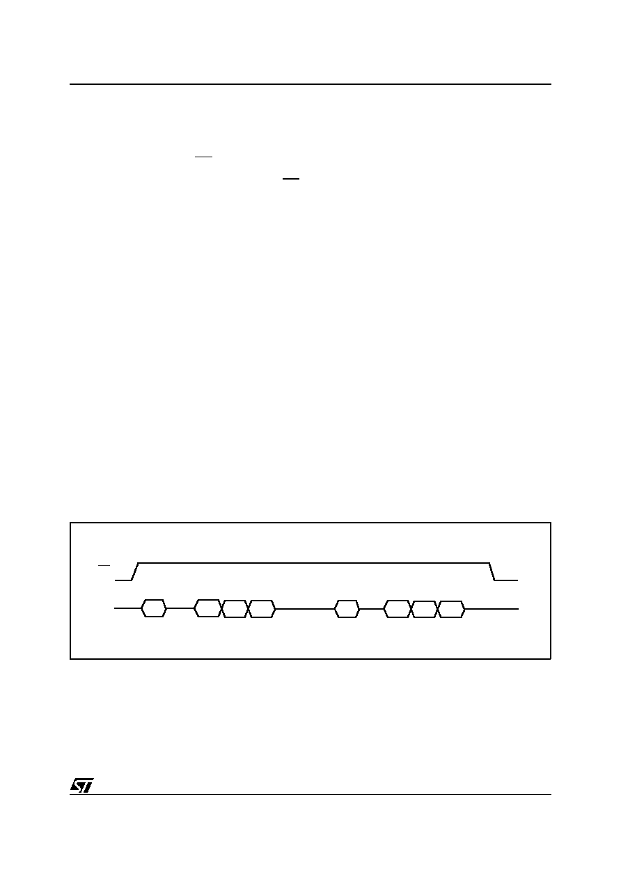
33/59
NAND512-B, NAND01G-B, NAND02G-B, NAND04G-B, NAND08G-B
DATA PROTECTION
The device has both hardware and software fea-
tures to protect against program and erase opera-
tions.
It features a Write Protect, WP, pin, which can be
used to protect the device against program and
erase operations. It is recommended to keep WP
at V
IL
during power-up and power-down.
In addition, to protect the memory from any invol-
untary program/erase operations during power-
transitions, the device has an internal voltage de-
tector which disables all functions whenever V
CC
is below 1.5V.
The device features a Block Lock mode, which is
enabled by setting the Power-Up Read Enable,
Lock/Unlock Enable, PRL, signal to High.
The Block Lock mode has two levels of software
protection.
Blocks Lock/Unlock
Blocks Lock-down
Refer to
Figure 21.
for an overview of the protec-
tion mechanism.
Blocks Lock
All the blocks are locked simultaneously by issuing
a Blocks Lock command (see
Table 10.
).
All blocks are locked after power-up and when the
Write Protect signal is Low.
Once all the blocks are locked, one sequence of
consecutive blocks can be unlocked by using the
Blocks Unlock command.
Refer to
Figure 25., Command Latch AC Wave-
forms
for details on how to issue the command.
Blocks Unlock
A sequence of consecutive locked blocks can be
unlocked, to allow program or erase operations, by
issuing an Blocks Unlock command (see
Table
10.
).
The Blocks Unlock command consists of four
steps:
One bus cycle to setup the command
two or three bus cycles to give the Start Block
Address (refer to
Table 8.
,
Table 9.
and
Figure 19.
)
one bus cycle to confirm the command
two or three bus cycles to give the End Block
Address (refer to
Table 8.
,
Table 9.
and
Figure
19.
).
The Start Block Address must be nearer the logi-
cal LSB (Least Significant Bit) than End Block Ad-
dress.
If the Start Block Address is the same as the End
Block Address, only one block is unlocked.
Only one consecutive area of blocks can be un-
locked at any one time. It is not possible to unlock
multiple areas.
Figure 19. Blocks Unlock Operation
Note: Three address cycles are required for 2,4 and 8 Gb devices. The 512Mb and 1Gb devices only require two address cycles.
I/O
WP
Start Block Address, 3 cycles
ai08670
23h
Blocks Unlock
Command
Add1
Add2
Add3
24h
Add1
Add2
Add3
End Block Address, 3 cycles

NAND512-B, NAND01G-B, NAND02G-B, NAND04G-B, NAND08G-B
34/59
Blocks Lock-Down
The Lock-Down feature provides an additional lev-
el of protection. A Locked-down block cannot be
unlocked by a software command. Locked-Down
blocks can only be unlocked by setting the Write
Protect signal to Low for a minimum of 100ns.
Only locked blocks can be locked-down. The com-
mand has no affect on unlocked blocks.
Refer to
Figure 25., Command Latch AC Wave-
forms
for details on how to issue the command.
Block Lock Status
In Block Lock mode (PRL High) the Block Lock
Status of each block can be checked by issuing a
Read Block Lock Status command (see
Table
10.
).
The command consists of:
one bus cycle to give the command code
three bus cysles to give the block address
After this, a read cycle will then output the Block
Lock Status on the I/O pins on the falling edge of
Chip Enable or Read Enable, whichever occurs
last. Chip Enable or Read Enable do not need to
be toggled to update the status.
The Read Block Lock Status command will not be
accepted while the device is busy (RB Low).
The device will remain in Read Block Lock Status
mode until another command is issued.
If the device is not in the Block Lock mode (PRL
Low) the Block Status can be read in the Status
Register using the Read Status Register com-
mand.
Figure 20. Read Block Lock Status Operation
Note: Three address cycles are required for 2,4 and 8 Gb devices. The 512Mb and 1Gb devices only require two address cycles.
Table 16. Block Lock Status
Note: X = Don't Care.
Status
I/O7-I/O3
I/O2
I/O1
I/O0
Locked
X
0
1
0
Unlocked
X
1
1
0
Locked-Down
X
0
0
1
Unlocked in Locked-
Down Area
X
1
0
1
I/O
R
Block Address, 3 cycles
ai08669
7Ah
Read Block Lock
Status Command
Add1
Add2
Add3
Dout
Block Lock Status
tWHRL
W
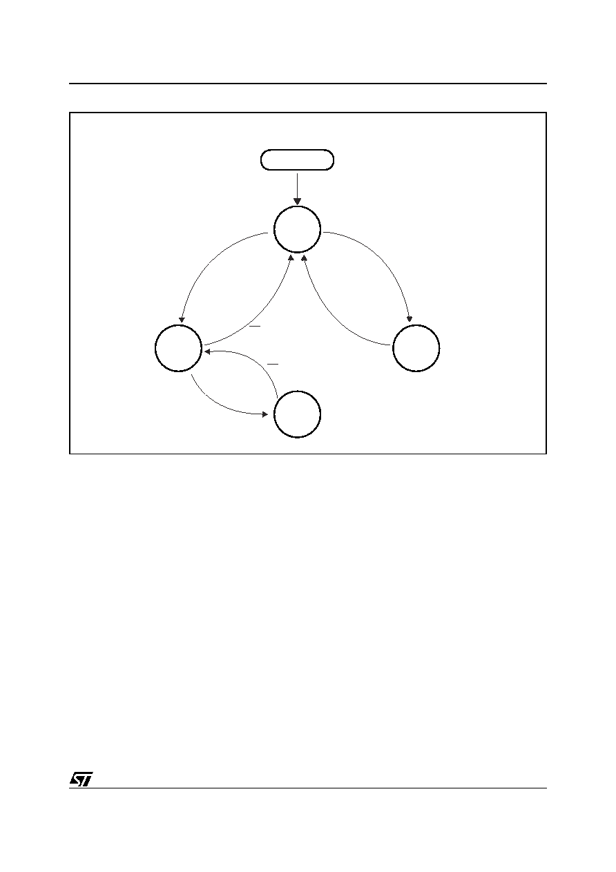
35/59
NAND512-B, NAND01G-B, NAND02G-B, NAND04G-B, NAND08G-B
Figure 21. Block Protection State Diagram
Note: PRL must be High for the software commands to be accepted.
AI08663b
Locked
Locked-Down
Unlocked in
Locked Area
Power-Up
Block Unlock
Command
Blocks Lock-Down
Command
WP VIL >100ns
Blocks Lock
Command
WP VIL >100ns
(start + end block address)
Unlocked in
Locked-Down
Area
Blocks Lock-Down
Command
WP VIL >100ns
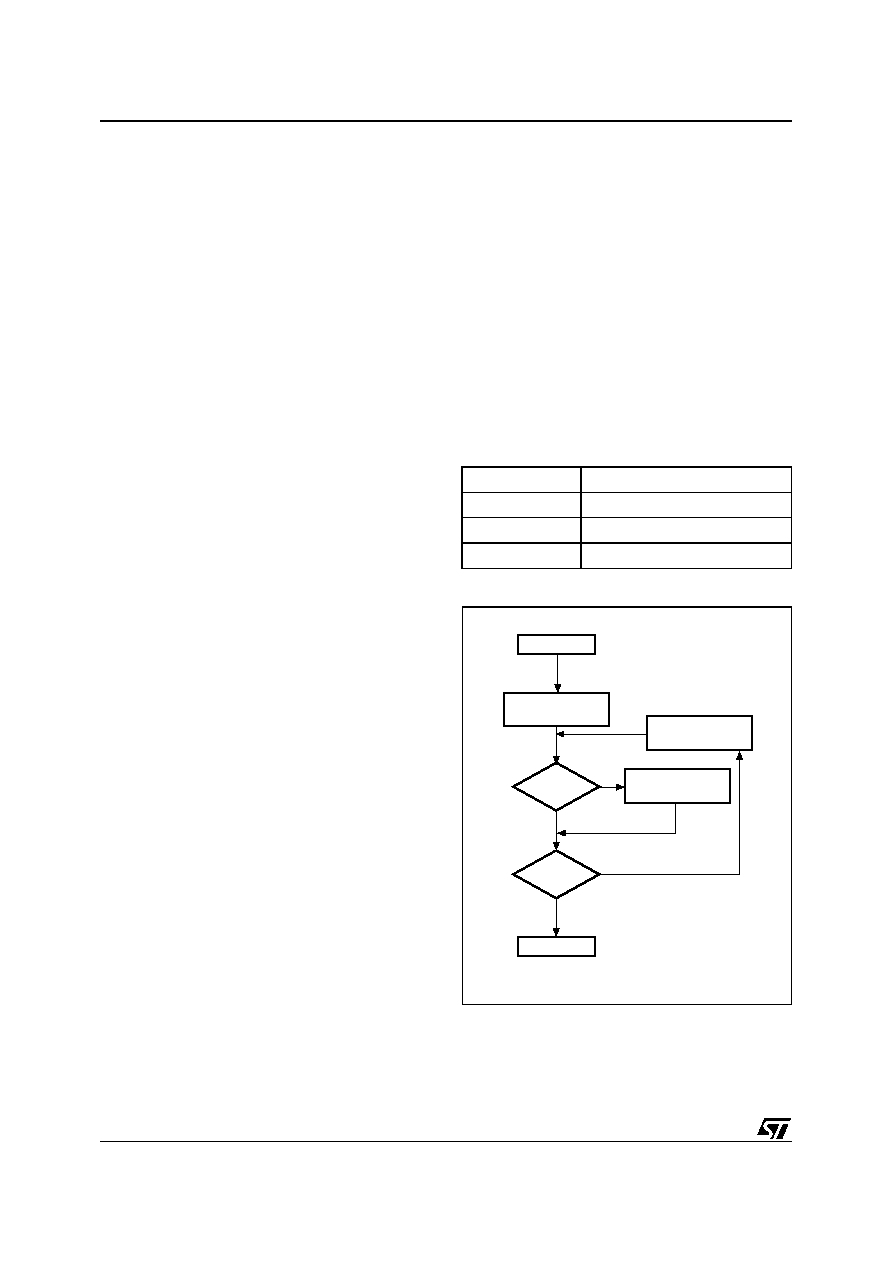
NAND512-B, NAND01G-B, NAND02G-B, NAND04G-B, NAND08G-B
36/59
SOFTWARE ALGORITHMS
This section gives information on the software al-
gorithms that ST recommends to implement to
manage the Bad Blocks and extend the lifetime of
the NAND device.
NAND Flash memories are programmed and
erased by Fowler-Nordheim tunneling using a high
voltage. Exposing the device to a high voltage for
extended periods can cause the oxide layer to be
damaged. For this reason, the number of program
and erase cycles is limited (see
Table 18.
for val-
ue) and it is recommended to implement Garbage
Collection, a Wear-Leveling Algorithm and an Er-
ror Correction Code, to extend the number of pro-
gram and erase cycles and increase the data
retention.
To help integrate a NAND memory into an applica-
tion ST Microelectronics can provide:
A Demo board with NAND simulation software
for PCs
File System OS Native reference software,
which supports the basic commands of file
management.
Contact the nearest ST Microelectronics sales of-
fice for more details.
Bad Block Management
Devices with Bad Blocks have the same quality
level and the same AC and DC characteristics as
devices where all the blocks are valid. A Bad Block
does not affect the performance of valid blocks be-
cause it is isolated from the bit line and common
source line by a select transistor.
The devices are supplied with all the locations in-
side valid blocks erased (FFh). The Bad Block In-
formation is written prior to shipping. Any block,
where the 1st and 6th Bytes, or 1st Word,
in the
spare area of the 1st page, does not contain FFh,
is a Bad Block.
The Bad Block Information must be read before
any erase is attempted as the Bad Block Informa-
tion may be erased. For the system to be able to
recognize the Bad Blocks based on the original in-
formation it is recommended to create a Bad Block
table following the flowchart shown in
Figure 22.
Block Replacement
Over the lifetime of the device additional Bad
Blocks may develop. In this case the block has to
be replaced by copying the data to a valid block.
These additional Bad Blocks can be identified as
attempts to program or erase them will give errors
in the Status Register.
As the failure of a page program operation does
not affect the data in other pages in the same
block, the block can be replaced by re-program-
ming the current data and copying the rest of the
replaced block to an available valid block. The
Copy Back Program command can be used to
copy the data to a valid block.
See the "
Copy Back Program
" section for more de-
tails.
Refer to
Table 17.
for the recommended proce-
dure to follow if an error occurs during an opera-
tion.
Table 17. Block Failure
Figure 22. Bad Block Management Flowchart
Operation
Recommended Procedure
Erase
Block Replacement
Program
Block Replacement or ECC
Read
ECC
AI07588C
START
END
NO
YES
YES
NO
Block Address =
Block 0
Data
= FFh?
Last
block?
Increment
Block Address
Update
Bad Block table

37/59
NAND512-B, NAND01G-B, NAND02G-B, NAND04G-B, NAND08G-B
Figure 23. Garbage Collection
Garbage Collection
When a data page needs to be modified, it is faster
to write to the first available page, and the previous
page is marked as invalid. After several updates it
is necessary to remove invalid pages to free some
memory space.
To free this memory space and allow further pro-
gram operations it is recommended to implement
a Garbage Collection algorithm. In a Garbage Col-
lection software the valid pages are copied into a
free area and the block containing the invalid pag-
es is erased (see
Figure 23.
).
Wear-leveling Algorithm
For write-intensive applications, it is recommend-
ed to implement a Wear-leveling Algorithm to
monitor and spread the number of write cycles per
block.
In memories that do not use a Wear-Leveling Al-
gorithm not all blocks get used at the same rate.
Blocks with long-lived data do not endure as many
write cycles as the blocks with frequently-changed
data.
The Wear-leveling Algorithm ensures that equal
use is made of all the available write cycles for
each block. There are two wear-leveling levels:
First Level Wear-leveling, new data is
programmed to the free blocks that have had
the fewest write cycles
Second Level Wear-leveling, long-lived data is
copied to another block so that the original
block can be used for more frequently-
changed data.
The Second Level Wear-leveling is triggered when
the difference between the maximum and the min-
imum number of write cycles per block reaches a
specific threshold.
Error Correction Code
An Error Correction Code (ECC) can be imple-
mented in the Nand Flash memories to identify
and correct errors in the data.
For every 2048 bits in the device it is recommend-
ed to implement 22 bits of ECC (16 bits for line par-
ity plus 6 bits for column parity).
An ECC model is available in VHDL or Verilog.
Contact the nearest ST Microelectronics sales of-
fice for more details.
Figure 24. Error Detection
Valid
Page
Invalid
Page
Free
Page
(Erased)
Old Area
AI07599B
New Area (After GC)
New ECC generated
during read
XOR previous ECC
with new ECC
All results
= zero?
22 bit data = 0
YES
11 bit data = 1
NO
1 bit data = 1
Correctable
Error
ECC Error
No Error
ai08332
>1 bit
= zero?
YES
NO

NAND512-B, NAND01G-B, NAND02G-B, NAND04G-B, NAND08G-B
38/59
Hardware Simulation Models
Behavioral simulation models. Denali Software
Corporation models are platform independent
functional models designed to assist customers in
performing entire system simulations (typical
VHDL/Verilog). These models describe the logic
behavior and timings of NAND Flash devices, and
so allow software to be developed before hard-
ware.
IBIS simulations models. IBIS (I/O Buffer Infor-
mation Specification) models describe the behav-
ior of the I/O buffers and electrical characteristics
of Flash devices.
These models provide information such as AC
characteristics, rise/fall times and package me-
chanical data, all of which are measured or simu-
lated at voltage and temperature ranges wider
than those allowed by target specifications.
IBIS models are used to simulate PCB connec-
tions and can be used to resolve compatibility is-
sues when upgrading devices. They can be
imported into SPICETOOLS.

39/59
NAND512-B, NAND01G-B, NAND02G-B, NAND04G-B, NAND08G-B
PROGRAM AND ERASE TIMES AND ENDURANCE CYCLES
The Program and Erase times and the number of
Program/ Erase cycles per block are shown in
Ta-
ble 18.
Table 18. Program, Erase Times and Program Erase Endurance Cycles
MAXIMUM RATING
Stressing the device above the ratings listed in
Ta-
ble 19., Absolute Maximum Ratings
, may cause
permanent damage to the device. These are
stress ratings only and operation of the device at
these or any other conditions above those indicat-
ed in the Operating sections of this specification is
not implied. Exposure to Absolute Maximum Rat-
ing conditions for extended periods may affect de-
vice reliability. Refer also to the
STMicroelectronics SURE Program and other rel-
evant quality documents.
Table 19. Absolute Maximum Ratings
Note: 1. Minimum Voltage may undershoot to ≠2V for less than 20ns during transitions on input and I/O pins. Maximum voltage may over-
shoot to V
DD
+ 2V for less than 20ns during transitions on I/O pins.
Parameters
NAND Flash
Unit
Min
Typ
Max
Page Program Time
300
700
µs
Block Erase Time
2
3
ms
Program/Erase Cycles (per block)
100,000
cycles
Data Retention
10
years
Symbol
Parameter
Value
Unit
Min
Max
T
BIAS
Temperature Under Bias
≠
50
125
∞C
T
STG
Storage Temperature
≠
65
150
∞C
V
IO
(1)
Input or Output Voltage
1.8V devices
≠
0.6
2.7
V
3 V devices
≠
0.6
4.6
V
V
DD
Supply Voltage
1.8V devices
≠
0.6
2.7
V
3 V devices
≠
0.6
4.6
V
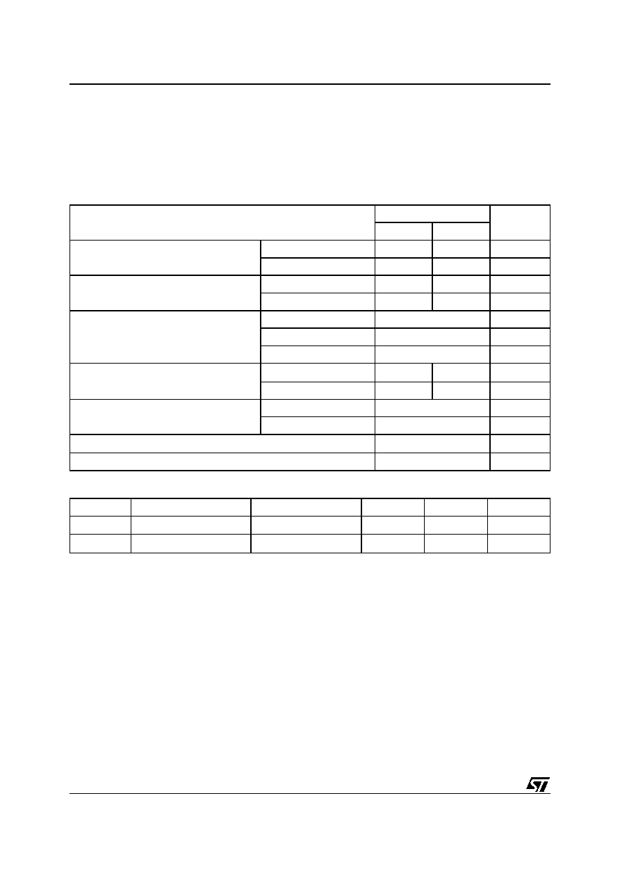
NAND512-B, NAND01G-B, NAND02G-B, NAND04G-B, NAND08G-B
40/59
DC AND AC PARAMETERS
This section summarizes the operating and mea-
surement conditions, and the DC and AC charac-
teristics of the device. The parameters in the DC
and AC characteristics Tables that follow, are de-
rived from tests performed under the Measure-
ment Conditions summarized in
Table
20., Operating and AC Measurement Conditions
.
Designers should check that the operating condi-
tions in their circuit match the measurement condi-
tions when relying on the quoted parameters.
Table 20. Operating and AC Measurement Conditions
Table 21. Capacitance
Note: T
A
= 25∞C, f = 1 MHz. C
IN
and C
I/O
are not 100% tested.
Parameter
NAND Flash
Units
Min
Max
Supply Voltage (V
DD
)
1.8V devices
1.7
1.95
V
3V devices
2.7
3.6
V
Ambient Temperature (T
A
)
Grade 1
0
70
∞C
Grade 6
≠40
85
∞C
Load Capacitance (C
L
) (1 TTL GATE and C
L
)
1.8V devices
30
pF
3V devices (2.7 - 3.6V)
50
pF
3V devices (3.0 - 3.6V)
100
pF
Input Pulses Voltages
1.8V devices
0
V
DD
V
3V devices
0.4
2.4
V
Input and Output Timing Ref. Voltages
1.8V devices
0.9
V
3V devices
1.5
V
Output Circuit Resistor R
ref
8.35
k
Input Rise and Fall Times
5
ns
Symbol
Parameter
Test Condition
Typ
Max
Unit
C
IN
Input Capacitance
V
IN
= 0V
10
pF
C
I/O
Input/Output Capacitance
V
IL
= 0V
10
pF

41/59
NAND512-B, NAND01G-B, NAND02G-B, NAND04G-B, NAND08G-B
Table 22. DC Characteristics, 1.8V Devices
Symbol
Parameter
Test Conditions
Min
Typ
Max
Unit
I
DD1
Operating
Current
Sequential
Read
t
RLRL
minimum
E=V
IL,
I
OUT
= 0 mA
-
8
15
mA
I
DD2
Program
-
-
8
15
mA
I
DD3
Erase
-
-
8
15
mA
I
DD5
Standby Current (CMOS)
E=V
DD
-0.2,
WP=0/V
DD
-
10
50
µA
I
LI
Input Leakage Current
V
IN
= 0 to V
DD
max
-
-
±10
µA
I
LO
Output Leakage Current
V
OUT
= 0 to V
DD
max
-
-
±10
µA
V
IH
Input High Voltage
-
V
DD
-0.4
-
V
DD
+0.3
V
V
IL
Input Low Voltage
-
-0.3
-
0.4
V
V
OH
Output High Voltage Level
I
OH
= -100µA
V
DD
-0.1
-
-
V
V
OL
Output Low Voltage Level
I
OL
= 100µA
-
-
0.1
V
I
OL
(RB)
Output Low Current (RB)
V
OL
= 0.1V
3
4
mA
V
LKO
V
DD
Supply Voltage (Erase and
Program lockout)
-
-
-
1.5
V
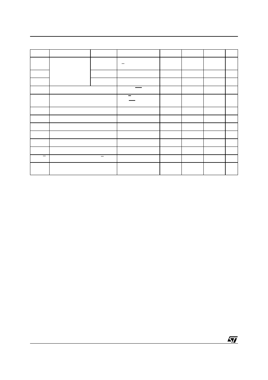
NAND512-B, NAND01G-B, NAND02G-B, NAND04G-B, NAND08G-B
42/59
Table 23. DC Characteristics, 3V Devices
Symbol
Parameter
Test Conditions
Min
Typ
Max
Unit
I
DD1
Operating
Current
Sequential
Read
t
RLRL
minimum
E=V
IL,
I
OUT
= 0 mA
-
10
20
mA
I
DD2
Program
-
-
10
20
mA
I
DD3
Erase
-
-
10
20
mA
I
DD4
Standby current (TTL)
E=V
IH
, WP=0/V
DD
1
mA
I
DD5
Standby Current (CMOS)
E=V
DD
-0.2,
WP=0/V
DD
-
10
50
µA
I
LI
Input Leakage Current
V
IN
= 0 to V
DD
max
-
-
±10
µA
I
LO
Output Leakage Current
V
OUT
= 0 to V
DD
max
-
-
±10
µA
V
IH
Input High Voltage
-
2.0
-
V
DD
+0.3
V
V
IL
Input Low Voltage
-
-0.3
-
0.8
V
V
OH
Output High Voltage Level
I
OH
= -100µA
2.4
-
-
V
V
OL
Output Low Voltage Level
I
OL
= 100µA
-
-
0.4
V
I
OL
(RB)
Output Low Current (RB)
V
OL
= 0.4V
8
10
mA
V
LKO
V
DD
Supply Voltage (Erase and
Program lockout)
-
-
-
2.5
V

43/59
NAND512-B, NAND01G-B, NAND02G-B, NAND04G-B, NAND08G-B
Table 24. AC Characteristics for Command, Address, Data Input
Note: 1. If t
ELWL
is less than 10ns, t
WLWH
must be minimum 35ns, otherwise, t
WLWH
may be minimum 25ns.
Symbol
Alt.
Symbol
Parameter
1.8V
Devices
3V
Devices
Unit
t
ALLWL
t
ALS
Address Latch Low to Write Enable Low
AL Setup time
Min
0
0
ns
t
ALHWL
Address Latch High to Write Enable Low
t
CLHWL
t
CLS
Command Latch High to Write Enable Low
CL Setup time
Min
0
0
ns
t
CLLWL
Command Latch Low to Write Enable Low
t
DVWH
t
DS
Data Valid to Write Enable High
Data Setup time
Min
20
20
ns
t
ELWL
t
CS
Chip Enable Low to Write Enable Low
E Setup time
Min
0
0
ns
t
WHALH
t
ALH
Write Enable High to Address Latch High
AL Hold time
Min
10
10
ns
t
WHCLH
t
CLH
Write Enable High to Command Latch High
CL hold time
Min
10
10
ns
t
WHCLL
Write Enable High to Command Latch Low
t
WHDX
t
DH
Write Enable High to Data Transition
Data Hold time
Min
10
10
ns
t
WHEH
t
CH
Write Enable High to Chip Enable High
E Hold time
Min
10
10
ns
t
WHWL
t
WH
Write Enable High to Write Enable Low
W High Hold
time
Min
20
20
ns
t
WLWH
t
WP
Write Enable Low to Write Enable High
W Pulse Width
Min
25
(1)
25
(1)
ns
t
WLWL
t
WC
Write Enable Low to Write Enable Low
Write Cycle time
Min
60
50
ns
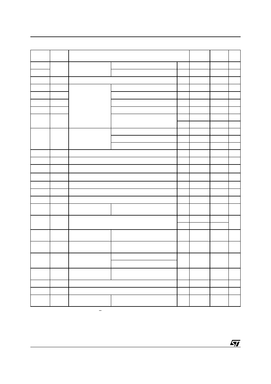
NAND512-B, NAND01G-B, NAND02G-B, NAND04G-B, NAND08G-B
44/59
Table 25. AC Characteristics for Operations
Note: 1. The time to Ready depends on the value of the pull-up resistor tied to the Ready/Busy pin. See Figures
35
,
36
and
37
.
2. To break the sequential read cycle, E must be held High for longer than t
EHEL
.
3. ES = Electronic Signature.
Symbol
Alt.
Symbol
Parameter
1.8V
Devices
3V
Devices
Unit
t
ALLRL1
t
AR
Address Latch Low to
Read Enable Low
Read Electronic Signature
Min
10
10
ns
t
ALLRL2
Read cycle
Min
10
10
ns
t
BHRL
t
RR
Ready/Busy High to Read Enable Low
Min
20
20
ns
t
BLBH1
Ready/Busy Low to
Ready/Busy High
Read Busy time
Max
25
25
µs
t
BLBH2
t
PROG
Program Busy time
Max
700
700
µs
t
BLBH3
t
BERS
Erase Busy time
Max
3
3
ms
t
BLBH4
Reset Busy time, during ready
Max
5
5
µs
t
BLBH5
t
CBSY
Cache Busy time
Typ
3
3
µs
Max
500
500
µs
t
WHBH1
t
RST
Write Enable High to
Ready/Busy High
Reset Busy time, during read
Max
5
5
µs
Reset Busy time, during program
Max
10
10
µs
Reset Busy time, during erase
Max
500
500
µs
t
CLLRL
t
CLR
Command Latch Low to Read Enable Low
Min
10
10
ns
t
DZRL
t
IR
Data Hi-Z to Read Enable Low
Min
0
0
ns
t
EHBH
t
CRY
Chip Enable High to Ready/Busy High (E intercepted read)
Max
60 + t
r
(1)
60 + t
r
(1)
ns
t
EHEL
t
CEH
Chip Enable High to Chip Enable Low
(2)
Min
100
100
ns
t
EHQZ
t
CHZ
Chip Enable High to Output Hi-Z
Max
20
20
ns
t
ELQV
t
CEA
Chip Enable Low to Output Valid
Max
45
45
ns
t
RHBL
t
RB
Read Enable High to Ready/Busy Low
Max
100
100
ns
t
RHRL
t
REH
Read Enable High to
Read Enable Low
Read Enable High Hold time
Min
20
20
ns
t
RHQZ
t
RHZ
Read Enable High to Output Hi-Z
Min
15
15
ns
Max
30
30
t
RLRH
t
RP
Read Enable Low to
Read Enable High
Read Enable Pulse Width
Min
25
25
ns
t
RLRL
t
RC
Read Enable Low to
Read Enable Low
Read Cycle time
Min
60
50
ns
t
RLQV
t
REA
Read Enable Low to
Output Valid
Read Enable Access time
Max
35
35
ns
Read ES Access time
(3)
t
WHBH
t
R
Write Enable High to
Ready/Busy High
Read Busy time
Max
25
25
µs
t
WHBL
t
WB
Write Enable High to Ready/Busy Low
Max
100
100
ns
t
WHRL
t
WHR
Write Enable High to Read Enable Low
Min
60
60
ns
t
WLWL
t
WC
Write Enable Low to
Write Enable Low
Write Cycle time
Min
60
50
ns
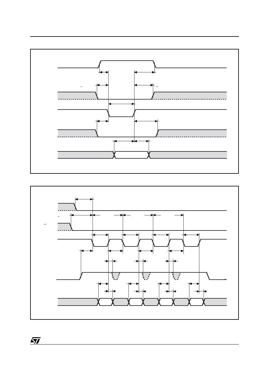
45/59
NAND512-B, NAND01G-B, NAND02G-B, NAND04G-B, NAND08G-B
Figure 25. Command Latch AC Waveforms
Figure 26. Address Latch AC Waveforms
Note: A fifth address cycle is required for 2Gb, 4Gb and 8Gb devices.
ai08028
CL
E
W
AL
I/O
tCLHWL
tELWL
tWHCLL
tWHEH
tWLWH
tALLWL
tWHALH
Command
tDVWH
tWHDX
(CL Setup time)
(CL Hold time)
(Data Setup time)
(Data Hold time)
(ALSetup time)
(AL Hold time)
(E Setup time)
(E Hold time)
ai08029
CL
E
W
AL
I/O
tWLWH
tELWL
tWLWL
tCLLWL
tWHWL
tALHWL
tDVWH
tWLWL
tWLWL
tWLWH
tWLWH
tWLWH
tWHWL
tWHWL
tWHDX
tWHALL
tDVWH
tWHDX
tDVWH
tWHDX
tDVWH
tWHDX
tWHALL
Adrress
cycle 1
tWHALL
(AL Setup time)
(AL Hold time)
Adrress
cycle 4
Adrress
cycle 3
Adrress
cycle 2
(CL Setup time)
(Data Setup time)
(Data Hold time)
(E Setup time)
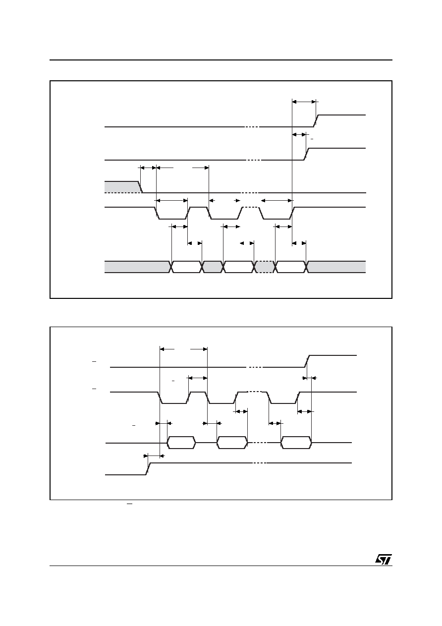
NAND512-B, NAND01G-B, NAND02G-B, NAND04G-B, NAND08G-B
46/59
Figure 27. Data Input Latch AC Waveforms
Note: Data In Last is 2112 in x8 devices and 1056 in x16 devices.
Figure 28. Sequential Data Output after Read AC Waveforms
Note: 1. CL = Low, AL = Low, W = High.
tWHCLH
CL
E
AL
W
I/O
tALLWL
tWLWL
tWLWH
tWHEH
tWLWH
tWLWH
Data In 0
Data In 1
Data In
Last
tDVWH
tWHDX
tDVWH
tWHDX
tDVWH
tWHDX
ai08030
(Data Setup time)
(Data Hold time)
(ALSetup time)
(CL Hold time)
(E Hold time)
E
ai08031
R
I/O
RB
tRLRL
tRLQV
tRHRL
tRLQV
Data Out
Data Out
Data Out
tRHQZ
tBHRL
tRLQV
tRHQZ
tEHQZ
(Read Cycle time)
(R Accesstime)
(R High Holdtime)

47/59
NAND512-B, NAND01G-B, NAND02G-B, NAND04G-B, NAND08G-B
Figure 29. Read Status Register AC Waveform
Figure 30. Read Electronic Signature AC Waveform
Note: 1. Refer to
Table 14.
for the values of the Manufacturer and Device Codes, and to
Table 15.
for the information contained in Byte4.
tELWL
tDVWH
Status Register
Output
70h/ 72h/
73h/ 74h/ 75h
CL
E
W
R
I/O
tCLHWL
tWHDX
tWLWH
tWHCLL
tCLLRL
tDZRL
tRLQV
tEHQZ
tRHQZ
tWHRL
tELQV
tWHEH
ai08666
(Data Setup time)
(Data Hold time)
90h
00h
Man.
code
Device
code
CL
E
W
AL
R
I/O
tRLQV
Read Electronic
Signature
Command
1st Cycle
Address
ai08667
(Read ES Access time)
tALLRL1
00h
Byte4
Byte3
Byte1
Byte2
see Note.1
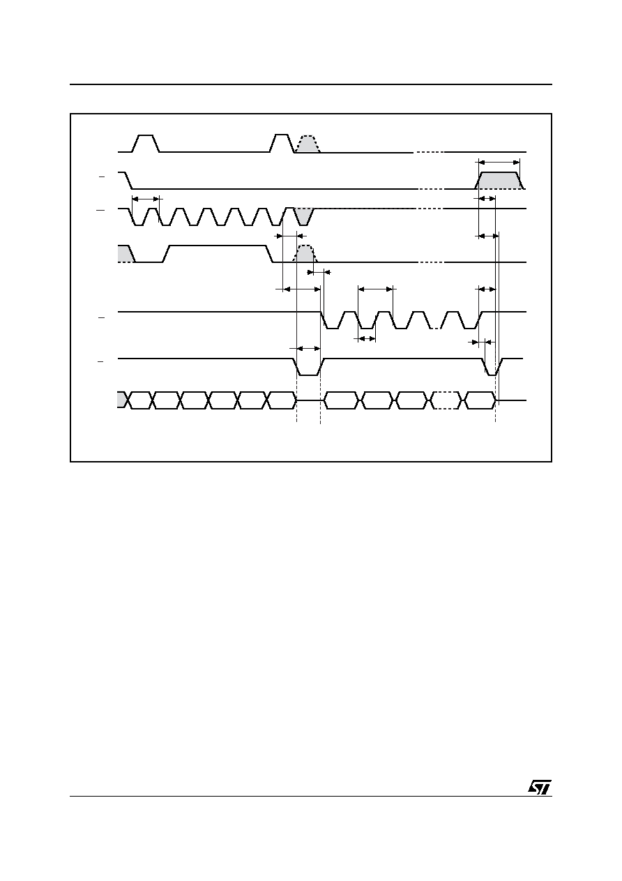
NAND512-B, NAND01G-B, NAND02G-B, NAND04G-B, NAND08G-B
48/59
Figure 31. Page Read Operation AC Waveform
Note: A fifth address cycle is required for 2Gb, 4Gb and 8Gb devices.
tEHEL
CL
E
W
AL
R
I/O
RB
tWLWL
tWHBL
tALLRL2
00h
Data
N
Data
N+1
Data
N+2
Data
Last
tRHBL
tEHBH
tWHBH
tRLRL
tEHQZ
tRHQZ
ai08660
Busy
Command
Code
Address N Input
Data Output
from Address N to Last Byte or Word in Page
Add.N
cycle 1
Add.N
cycle 4
Add.N
cycle 3
Add.N
cycle 2
(Read Cycle time)
tRLRH
tBLBH1
30h
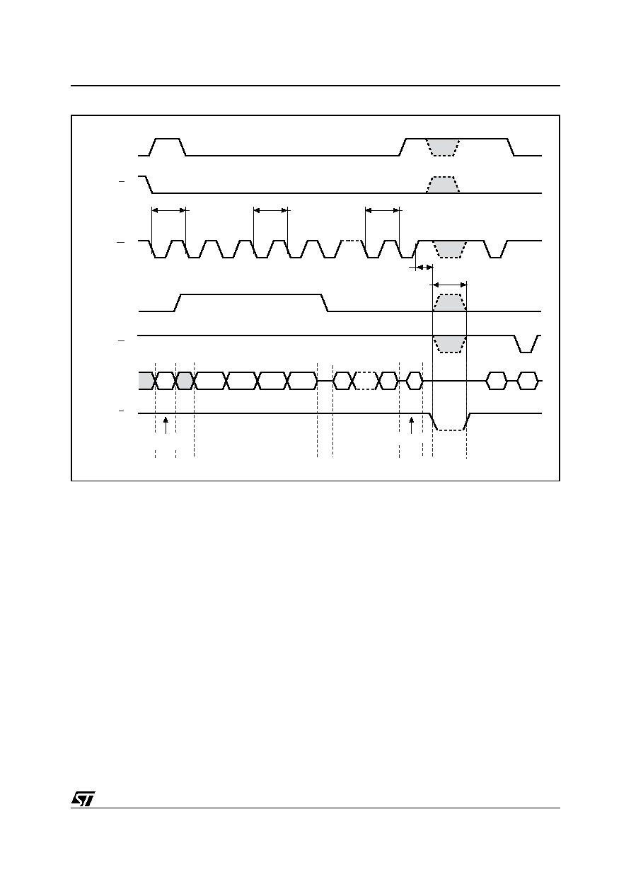
49/59
NAND512-B, NAND01G-B, NAND02G-B, NAND04G-B, NAND08G-B
Figure 32. Page Program AC Waveform
Note: A fifth address cycle is required for 2Gb, 4Gb and 8Gb devices.
CL
E
W
AL
R
I/O
RB
SR0
ai08668
N
Last
10h
70h
80h
Page Program
Setup Code
Confirm
Code
Read Status Register
tWLWL
tWLWL
tWLWL
tWHBL
tBLBH2
Page
Program
Address Input
Data Input
Add.N
cycle 1
Add.N
cycle 4
Add.N
cycle 3
Add.N
cycle 2
(Write Cycle time)
(Program Busy time)
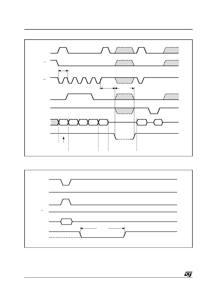
NAND512-B, NAND01G-B, NAND02G-B, NAND04G-B, NAND08G-B
50/59
Figure 33. Block Erase AC Waveform
Note: Address cycle 3 is required for 2Gb, 4Gb and 8Gb devices only.
Figure 34. Reset AC Waveform
D0h
60h
SR0
70h
ai08038b
tWHBL
tWLWL
tBLBH3
Block Erase
Setup Command
Block Erase
CL
E
W
AL
R
I/O
RB
Confirm
Code
Read Status Register
Block Address Input
(Erase Busy time)
(Write Cycle time)
Add.
cycle 1
Add.
cycle 3
Add.
cycle 2
W
R
I/O
RB
tBLBH4
AL
CL
FFh
ai08043
(Reset Busy time)
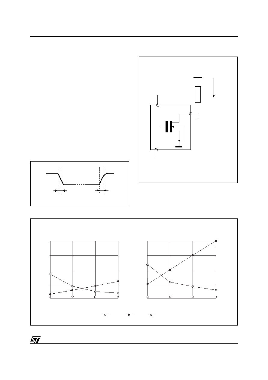
51/59
NAND512-B, NAND01G-B, NAND02G-B, NAND04G-B, NAND08G-B
Ready/Busy Signal Electrical Characteristics
Figures
36
,
35
and
37
show the electrical charac-
teristics for the Ready/Busy signal. The value re-
quired for the resistor R
P
can be calculated using
the following equation:
So,
where I
L
is the sum of the input currents of all the
devices tied to the Ready/Busy signal. R
P
max is
determined by the maximum value of t
r
.
Figure 35. Ready/Busy AC Waveform
Figure 36. Ready/Busy Load Circuit
Figure 37. Resistor Value Versus Waveform Timings For Ready/Busy Signal
Note: T = 25∞C.
RPmin
VDDmax VOLmax
≠
(
)
IOL
IL
+
------------------------------------------------------------
=
RPmin 1.8V
(
)
1.85V
3mA
IL
+
---------------------------
=
RPmin 3V
(
)
3.2V
8mA
IL
+
---------------------------
=
AI07564B
busy
VOH
ready VDD
VOL
tf
tr
AI07563B
RP
VDD
VSS
RB
DEVICE
Open Drain Output
ibusy
ai07565B
RP (K
)
1
2
3
4
100
300
200
t r
, t
f
(ns)
1
2
3
1.7
0.85
30
1.7
1.7
1.7
1.7
tr
tf
ibusy
0
400
4
RP (K
)
1
2
3
4
100
300
200
1
2
3
ibusy
(mA)
2.4
1.2
0.8
0.6
100
200
300
400
3.6
3.6
3.6
3.6
0
400
4
VDD = 1.8V, CL = 30pF
VDD = 3.3V, CL = 100pF
t r
, t
f
(ns)
ibusy
(mA)
60
90
120
0.57
0.43
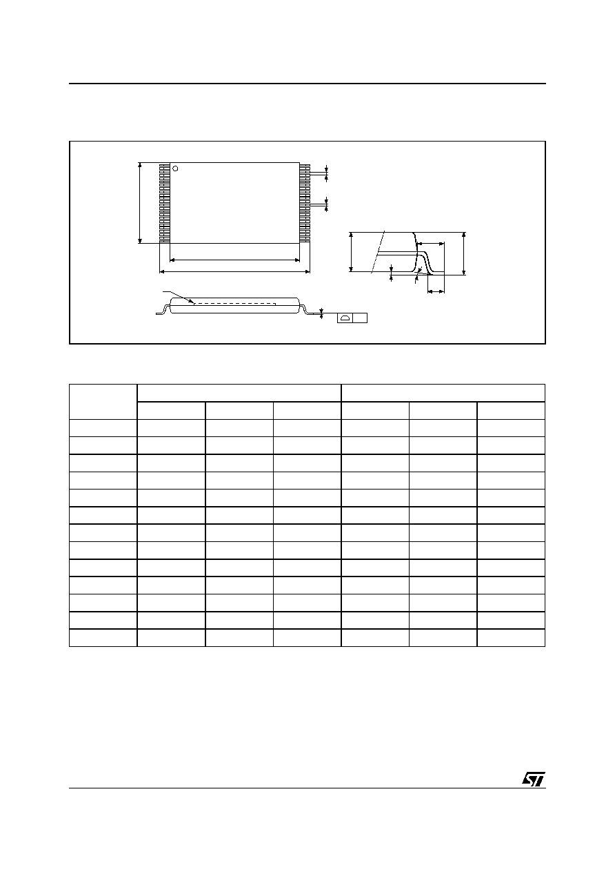
NAND512-B, NAND01G-B, NAND02G-B, NAND04G-B, NAND08G-B
52/59
PACKAGE MECHANICAL
Figure 38. TSOP48 - 48 lead Plastic Thin Small Outline, 12 x 20 mm, Package Outline
Note: Drawing is not to scale.
Table 26. TSOP48 - 48 lead Plastic Thin Small Outline, 12 x 20 mm, Package Mechanical Data
Symbol
millimeters
inches
Typ
Min
Max
Typ
Min
Max
A
1.200
0.0472
A1
0.100
0.050
0.150
0.0039
0.0020
0.0059
A2
1.000
0.950
1.050
0.0394
0.0374
0.0413
B
0.220
0.170
0.270
0.0087
0.0067
0.0106
C
0.100
0.210
0.0039
0.0083
CP
0.080
0.0031
D1
12.000
11.900
12.100
0.4724
0.4685
0.4764
E
20.000
19.800
20.200
0.7874
0.7795
0.7953
E1
18.400
18.300
18.500
0.7244
0.7205
0.7283
e
0.500
≠
≠
0.0197
≠
L
0.600
0.500
0.700
0.0236
0.0197
0.0276
L1
0.800
0.0315
3∞
0∞
5∞
3∞
0∞
5∞
TSOP-G
B
e
DIE
C
L
A1
E1
E
A
A2
1
24
48
25
D1
L1
CP
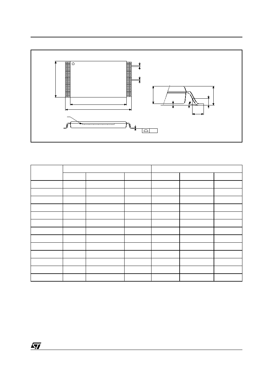
53/59
NAND512-B, NAND01G-B, NAND02G-B, NAND04G-B, NAND08G-B
Figure 39. USOP48 ≠ lead Plastic Ultra Thin Small Outline,12x17 mm, Package Outline
Note: Drawing not to scale.
Table 27. USOP48 ≠ lead Plastic Ultra Thin Small Outline, 12x17mm,
Package Mechanical Data
Symbol
millimeters
inches
Typ
Min
Max
Typ
Min
Max
A
0.48
0.65
0.019
0.026
A1
0.00
0.10
0.000
0.004
A2
0.52
0.48
0.56
0.020
0.019
0.022
b
0.16
0.13
0.23
0.006
0.005
0.009
c
0.10
0.08
0.17
0.004
0.003
0.007
D1
12.00
11.90
12.10
0.472
0.469
0.476
ddd
0.06
0.002
E
17.00
16.80
17.20
0.669
0.661
0.677
E1
15.40
15.30
15.50
0.606
0.602
0.610
e
0.50
≠
≠
0.020
≠
≠
L
0.55
0.45
0.65
0.022
0.018
0.026
L1
0.25
≠
≠
0.010
≠
≠
q
0
5
0
5
WSOP-A
b
e
DIE
c
A1
E1
E
A
A2
1
24
48
25
D1
ddd
L1
L
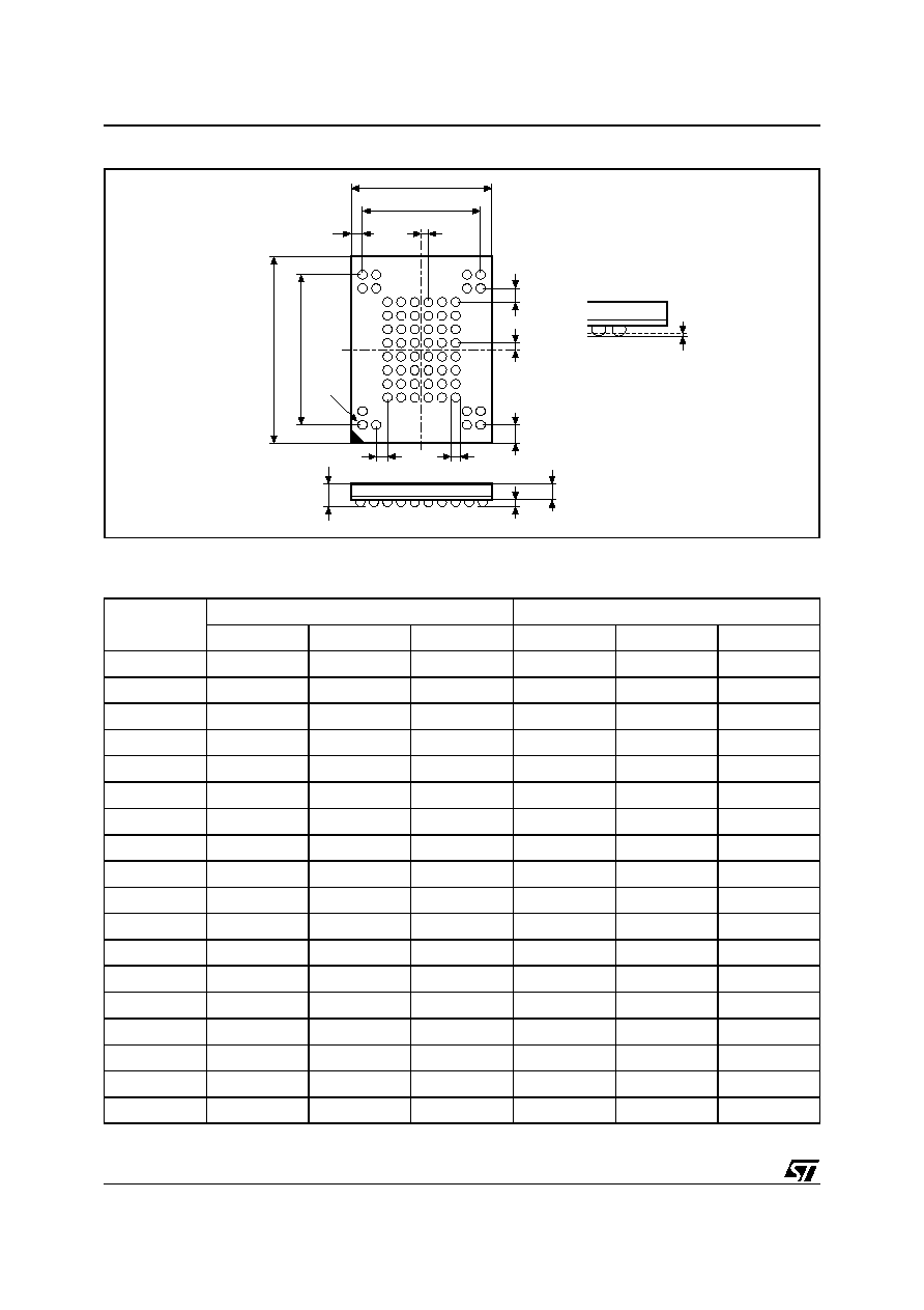
NAND512-B, NAND01G-B, NAND02G-B, NAND04G-B, NAND08G-B
54/59
Figure 40. VFBGA63 9.5x12mm - 6x8 active ball array, 0.80mm pitch, Package Outline
Note: Drawing is not to scale
Table 28. VFBGA63 9.5x12mm - 6x8 active ball array, 0.80mm pitch, Package Mechanical Data
Symbol
millimeters
inches
Typ
Min
Max
Typ
Min
Max
A
1.05
0.0413
A1
0.25
0.0098
A2
0.70
0.0276
b
0.45
0.40
0.50
0.0177
0.0157
0.0197
D
9.50
9.40
9.60
0.3740
0.3701
0.3780
D1
4.00
0.1575
D2
7.20
0.2835
ddd
0.10
0.0039
E
12.00
11.90
12.10
0.4724
0.4685
0.4764
E1
5.60
0.2205
E2
8.80
0.3465
e
0.80
≠
≠
0.0315
≠
≠
FD
2.75
0.1083
FD1
1.15
0.0453
FE
3.20
0.1260
FE1
1.60
0.0630
SD
0.40
0.0157
SE
0.40
0.0157
E
D
e
b
SD
SE
A2
A1
A
BGA-Z67
ddd
FD
D1
E1
e
FE
BALL "A1"
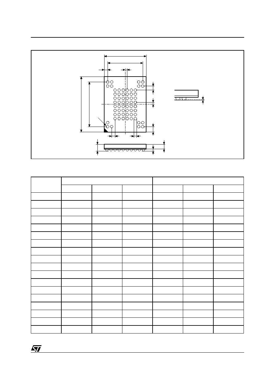
55/59
NAND512-B, NAND01G-B, NAND02G-B, NAND04G-B, NAND08G-B
Figure 41. TFBGA63 9.5x12mm - 6x8 active ball array, 0.80mm pitch, Package Outline
Note: Drawing is not to scale
Table 29. TFBGA63 9.5x12mm - 6x8 active ball array, 0.80mm pitch, Package Mechanical Data
Symbol
millimeters
inches
Typ
Min
Max
Typ
Min
Max
A
1.20
0.0472
A1
0.25
0.0098
A2
0.80
0.0315
b
0.45
0.40
0.50
0.0177
0.0157
0.0197
D
9.50
9.40
9.60
0.3740
0.3701
0.3780
D1
4.00
0.1575
D2
7.20
0.2835
ddd
0.10
0.0039
E
12.00
11.90
12.10
0.4724
0.4685
0.4764
E1
5.60
0.2205
E2
8.80
0.3465
e
0.80
≠
≠
0.0315
≠
≠
FD
2.75
0.1083
FD1
1.15
0.0453
FE
3.20
0.1260
FE1
1.60
0.0630
SD
0.40
0.0157
SE
0.40
0.0157
E
D
e
b
SD
SE
A2
A1
A
BGA-Z68
ddd
FD
D1
E1
e
FE
BALL "A1"
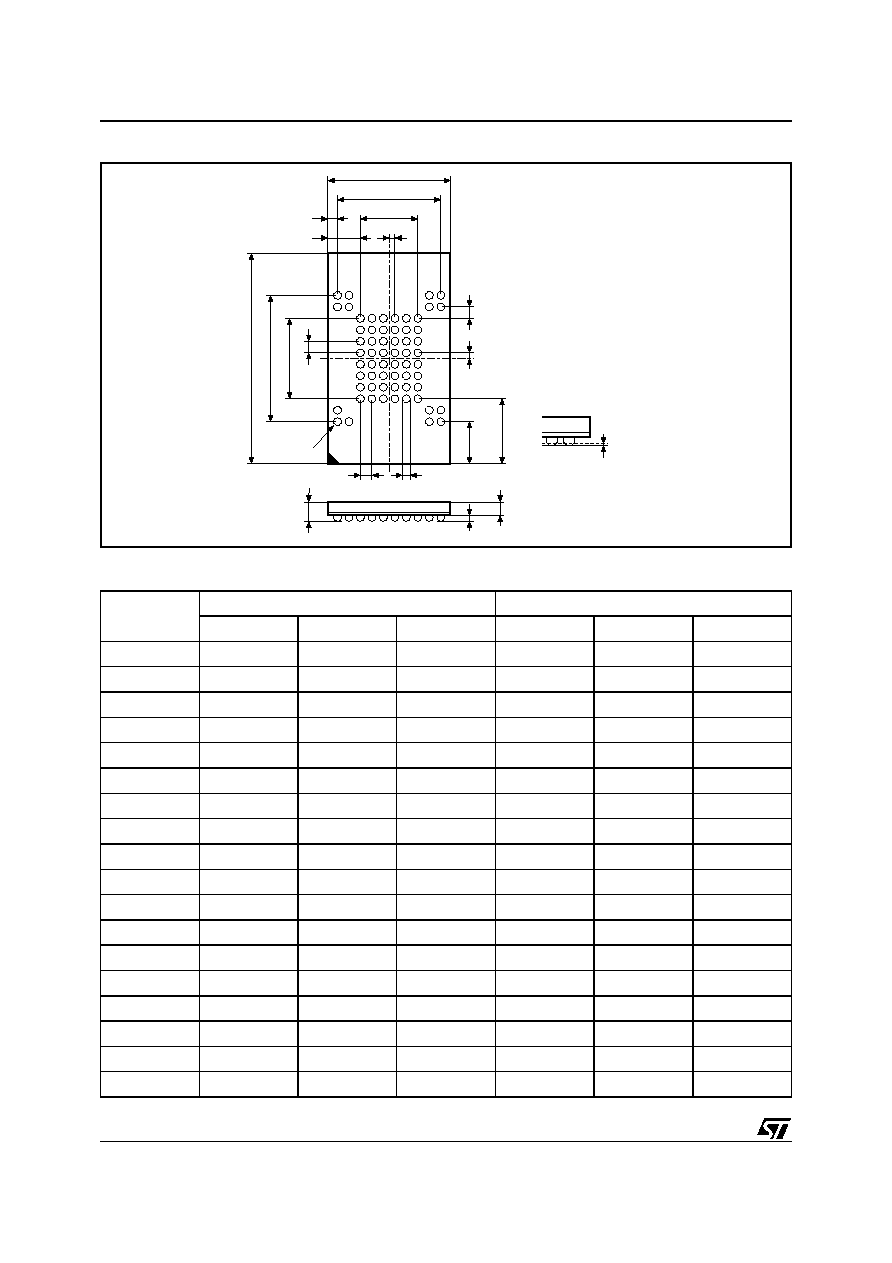
NAND512-B, NAND01G-B, NAND02G-B, NAND04G-B, NAND08G-B
56/59
Figure 42. LFBGA63 9.5x12mm - 6x8 active ball array, 0.80mm pitch, Package Outline
Table 30. LFBGA63 9.5x12mm - 6x8 active ball array, 0.80mm pitch, Package Mechanical Data
Symbol
millimeters
inches
Typ
Min
Max
Typ
Min
Max
A
1.400
0.0551
A1
0.250
0.0098
A2
0.800
0.0315
b
0.450
0.400
0.500
0.0177
0.0157
0.0197
D
8.500
8.400
8.600
0.3346
0.3307
0.3386
D1
4.000
0.1575
D2
7.200
0.2835
ddd
0.100
0.0039
E
15.000
14.900
15.100
0.5906
0.5866
0.5945
E1
5.600
0.2205
E2
8.800
0.3465
e
0.800
≠
≠
0.0315
≠
≠
FD
2.250
0.0886
FD1
0.650
0.0256
FE
4.700
0.1850
FE1
3.100
0.1220
SD
0.400
≠
≠
0.0157
≠
≠
SE
0.400
≠
≠
0.0157
≠
≠
E
D
e
b
SD
SE
A2
A1
A
BGA-Z59
ddd
FD1
D2
E2
e
FE
BALL "A1"
FE1
e
E1
D1
FD

57/59
NAND512-B, NAND01G-B, NAND02G-B, NAND04G-B, NAND08G-B
PART NUMBERING
Table 31. Ordering Information Scheme
Devices are shipped from the factory with the memory content bits, in valid blocks, erased to '1'. For further
information on any aspect of this device, please contact your nearest ST Sales Office.
Example:
NAND02GR3B
2
A ZA
1
T
Device Type
NAND Flash Memory
Density
512 = 512Mb
01G = 1Gb
02G = 2Gb
04G = 4Gb
08G = 8Gb
Operating Voltage
R = V
DD
= 1.7 to 1.95V
W = V
DD
= 2.7 to 3.6V
Bus Width
3 = x8
4 = x16
Family Identifier
B = 2112 Bytes/ 1056 Word Page
Device Options
2 = Chip Enable Don't Care Enabled
3 = Chip Enable Don't Care Enabled and Automatic Page 0 Read at Power-up
Product Version
A = First Version
B= Second Version
C= Third Version
Package
N = TSOP48 12 x 20mm (all devices)
V = USOP48 12 x 17 x 0.65mm (512Mb and 1Gb devices)
ZA = VFBGA63 9.5 x 12 x 1mm, 0.8mm pitch (512Mb and 1Gb devices)
ZB = TFBGA63 9.5 x 12 x 1.2mm, 0.8mm pitch (2Gb Dual Die devices)
ZC = LFBGA63 9.5 x 12 x 1.4mm, 0.8mm pitch (8Gb Quadruple Die devices)
Temperature Range
1 = 0 to 70 ∞C
6 = ≠40 to 85 ∞C
Option
blank = Standard Packing
T = Tape & Reel Packing
E = Lead Free Package, Standard Packing
F = Lead Free Package, Tape & Reel Packing

NAND512-B, NAND01G-B, NAND02G-B, NAND04G-B, NAND08G-B
58/59
REVISION HISTORY
Table 32. Document Revision History
Date
Version
Revision Details
25-Feb-2005
1
First Issue

59/59
NAND512-B, NAND01G-B, NAND02G-B, NAND04G-B, NAND08G-B
Information furnished is believed to be accurate and reliable. However, STMicroelectronics assumes no responsibility for the consequences
of use of such information nor for any infringement of patents or other rights of third parties which may result from its use. No license is granted
by implication or otherwise under any patent or patent rights of STMicroelectronics. Specifications mentioned in this publication are subject
to change without notice. This publication supersedes and replaces all information previously supplied. STMicroelectronics products are not
authorized for use as critical components in life support devices or systems without express written approval of STMicroelectronics.
The ST logo is a registered trademark of STMicroelectronics.
All other names are the property of their respective owners
© 2005 STMicroelectronics - All rights reserved
STMicroelectronics group of companies
Australia - Belgium - Brazil - Canada - China - Czech Republic - Finland - France - Germany - Hong Kong - India - Israel - Italy - Japan -
Malaysia - Malta - Morocco - Singapore - Spain - Sweden - Switzerland - United Kingdom - United States of America
www.st.com